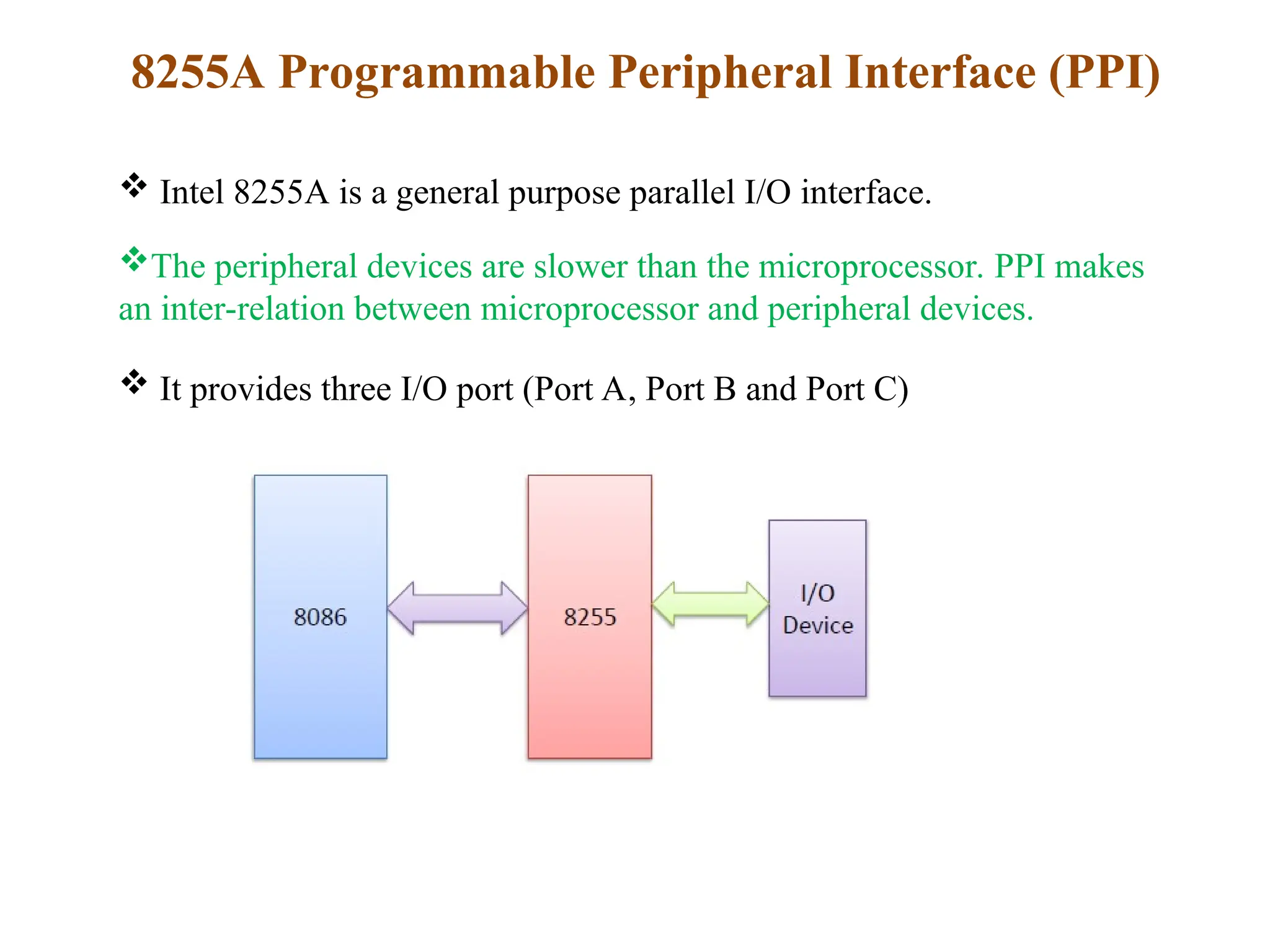
8255A Programmable PeripheralInterface (PPI)
Intel 8255A is a general purpose parallel I/O interface.
The peripheral devices are slower than the microprocessor. PPI makes
an inter-relation between microprocessor and peripheral devices.
It provides three I/O port (Port A, Port B and Port C)
3.
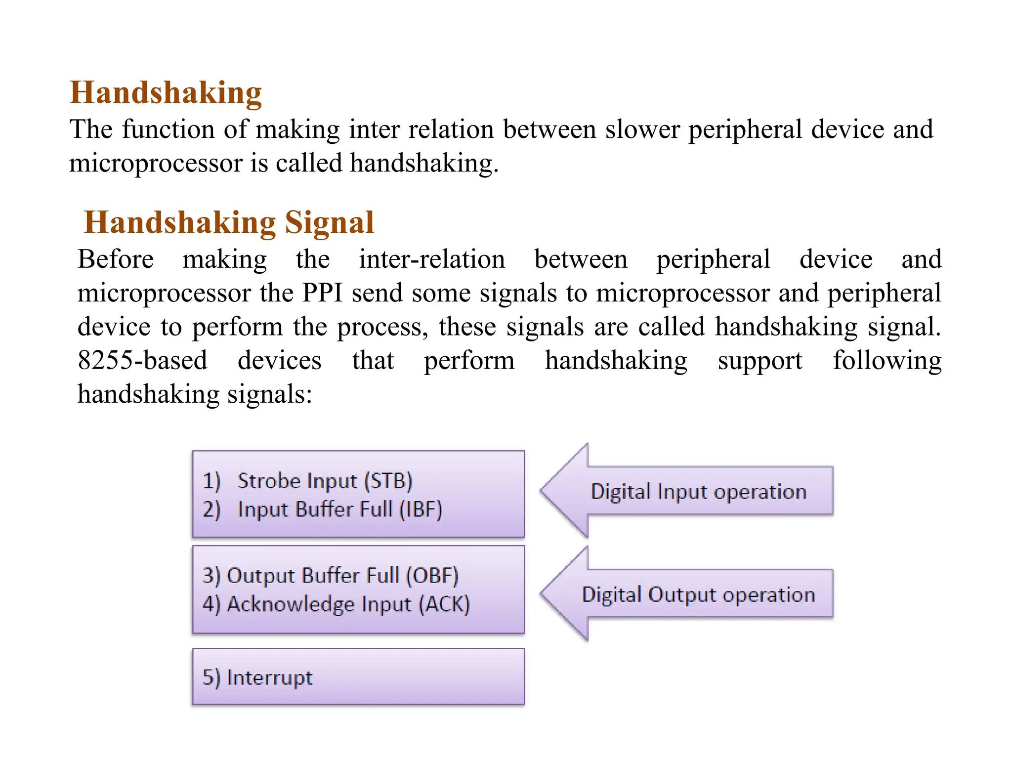
Handshaking
The function ofmaking inter relation between slower peripheral device and
microprocessor is called handshaking.
Handshaking Signal
Before making the inter-relation between peripheral device and
microprocessor the PPI send some signals to microprocessor and peripheral
device to perform the process, these signals are called handshaking signal.
8255-based devices that perform handshaking support following
handshaking signals:
4.
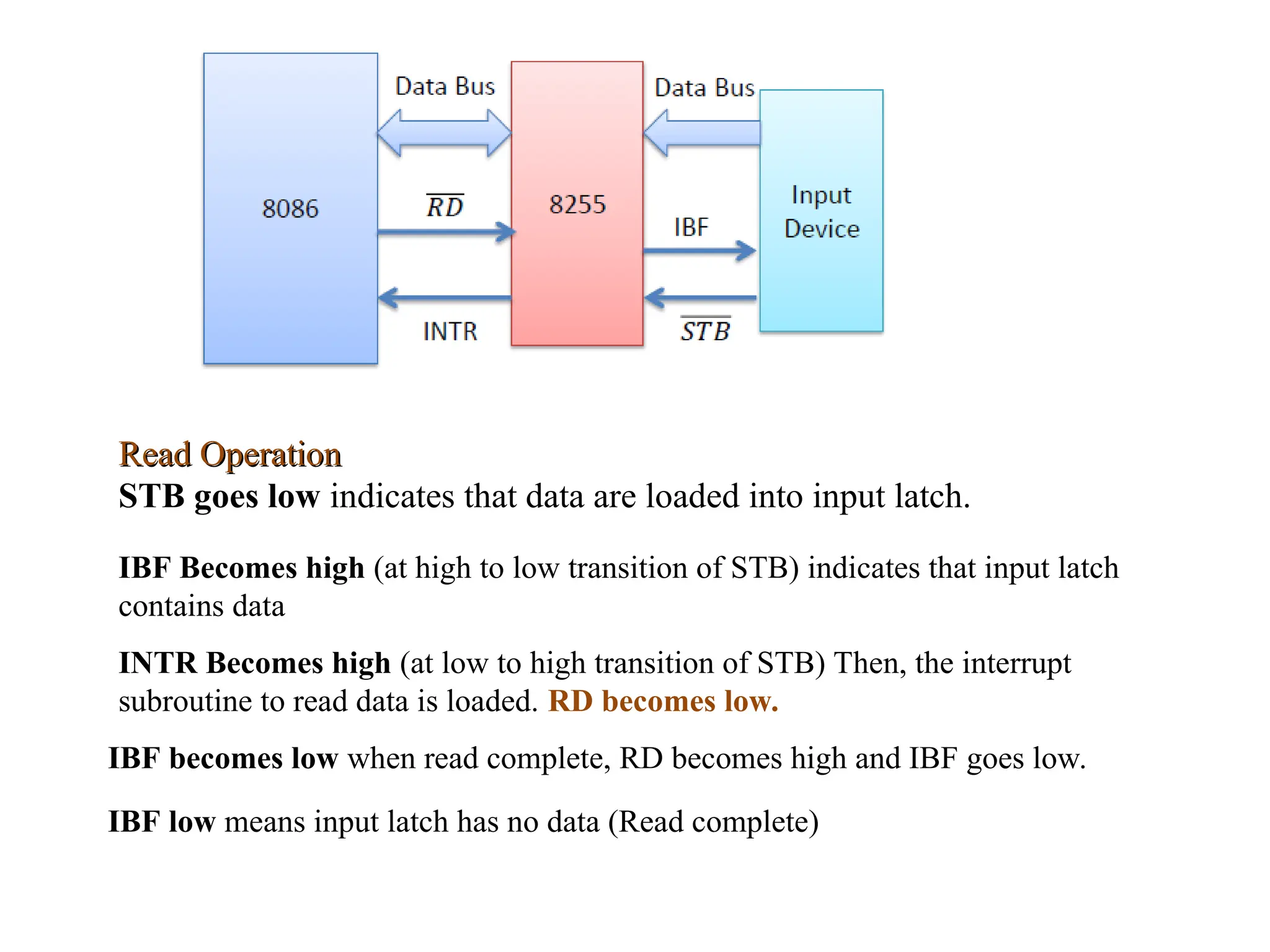
Read Operation
Read Operation
STBgoes low indicates that data are loaded into input latch.
IBF Becomes high (at high to low transition of STB) indicates that input latch
contains data
INTR Becomes high (at low to high transition of STB) Then, the interrupt
subroutine to read data is loaded. RD becomes low.
IBF becomes low when read complete, RD becomes high and IBF goes low.
IBF low means input latch has no data (Read complete)
5.
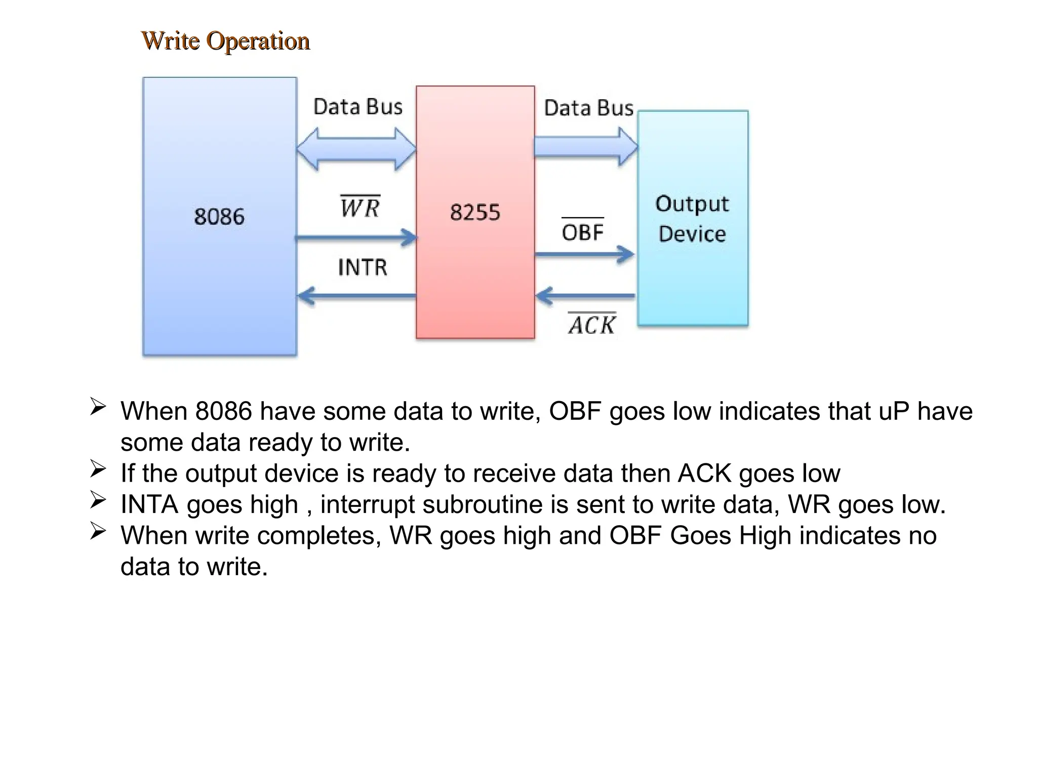
Write Operation
Write Operation
When 8086 have some data to write, OBF goes low indicates that uP have
some data ready to write.
If the output device is ready to receive data then ACK goes low
INTA goes high , interrupt subroutine is sent to write data, WR goes low.
When write completes, WR goes high and OBF Goes High indicates no
data to write.
7.
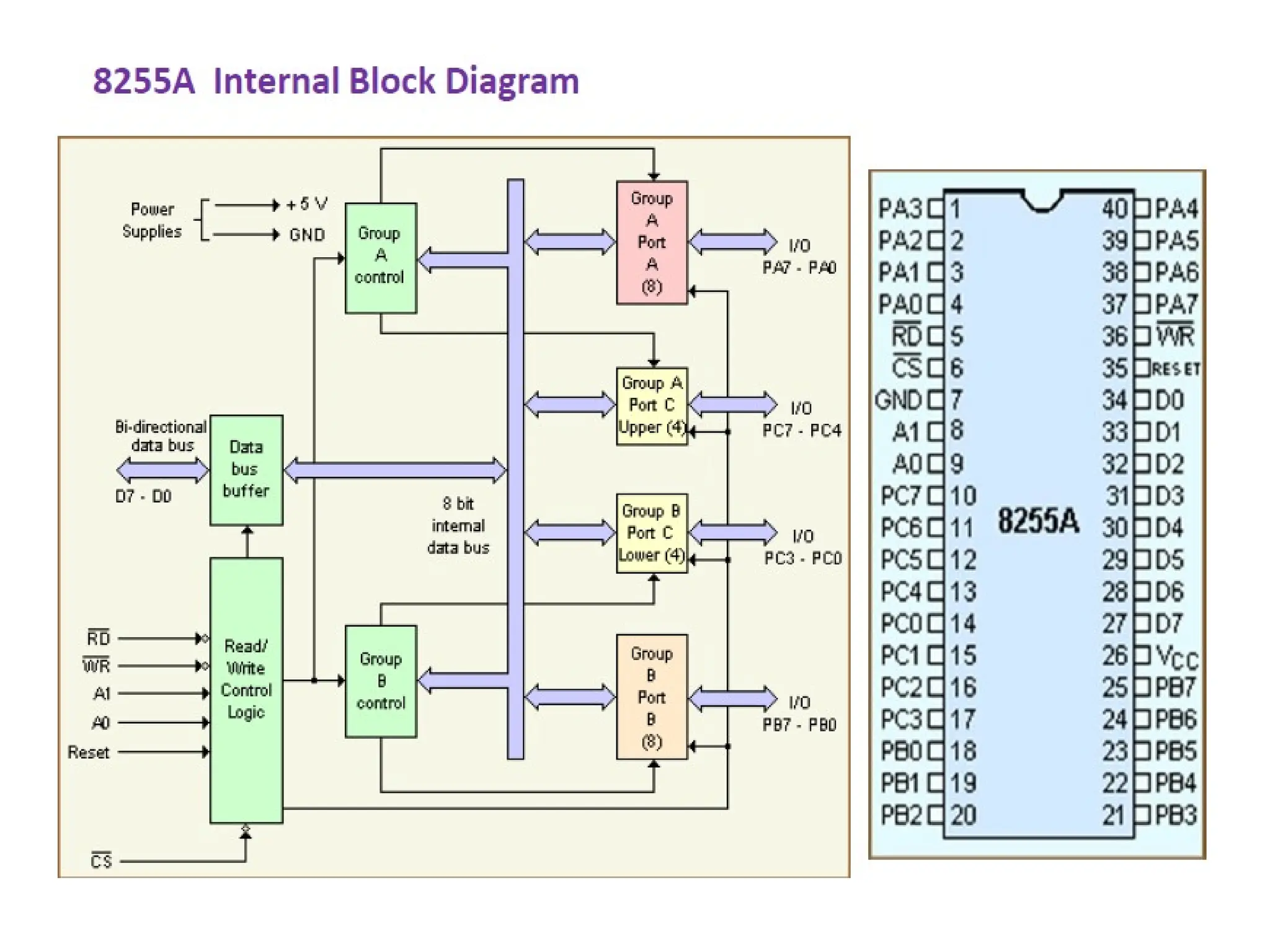
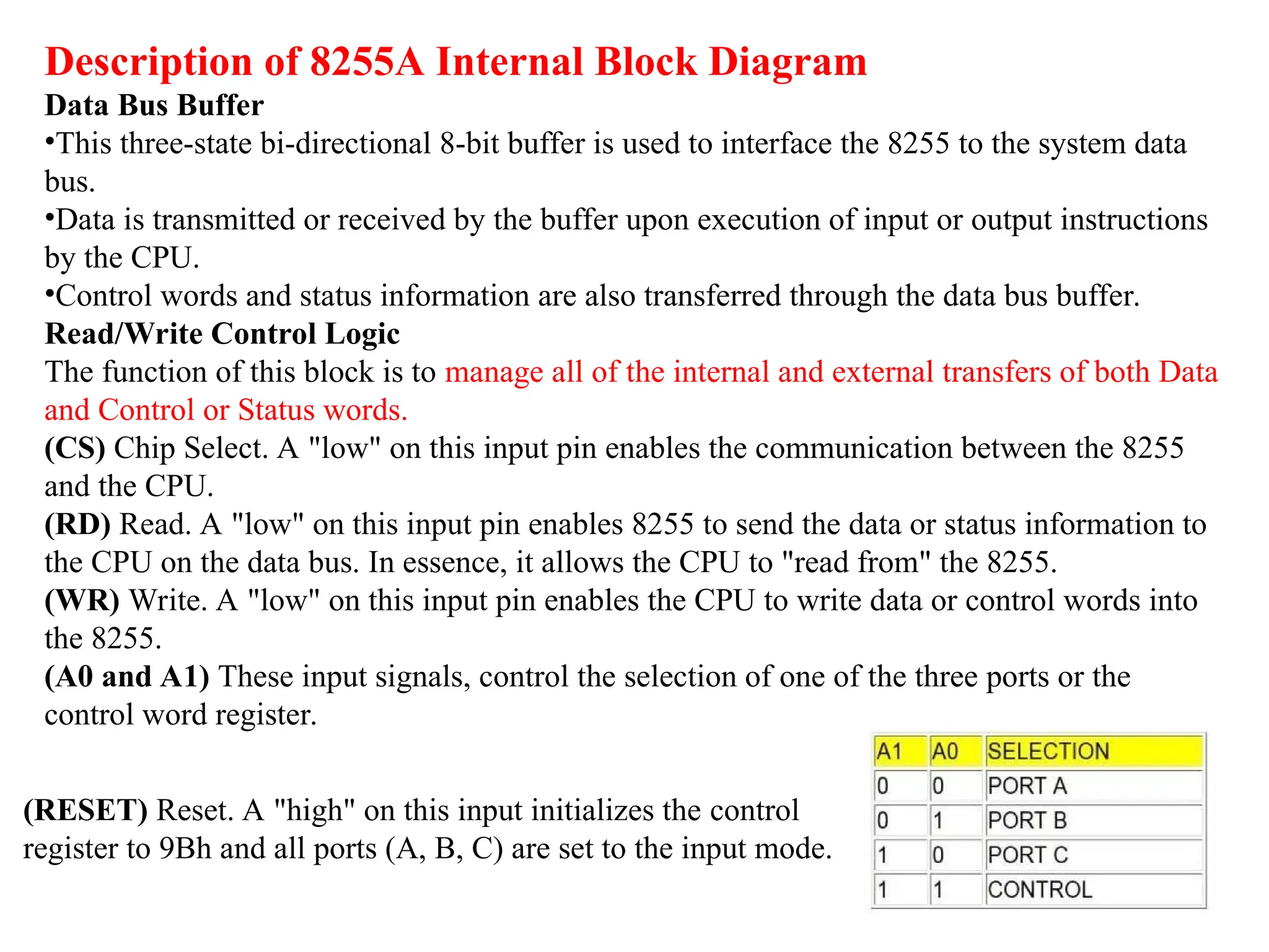
Description of 8255AInternal Block Diagram
Data Bus Buffer
•This three-state bi-directional 8-bit buffer is used to interface the 8255 to the system data
bus.
•Data is transmitted or received by the buffer upon execution of input or output instructions
by the CPU.
•Control words and status information are also transferred through the data bus buffer.
Read/Write Control Logic
The function of this block is to manage all of the internal and external transfers of both Data
and Control or Status words.
(CS) Chip Select. A "low" on this input pin enables the communication between the 8255
and the CPU.
(RD) Read. A "low" on this input pin enables 8255 to send the data or status information to
the CPU on the data bus. In essence, it allows the CPU to "read from" the 8255.
(WR) Write. A "low" on this input pin enables the CPU to write data or control words into
the 8255.
(A0 and A1) These input signals, control the selection of one of the three ports or the
control word register.
(RESET) Reset. A "high" on this input initializes the control
register to 9Bh and all ports (A, B, C) are set to the input mode.
8.
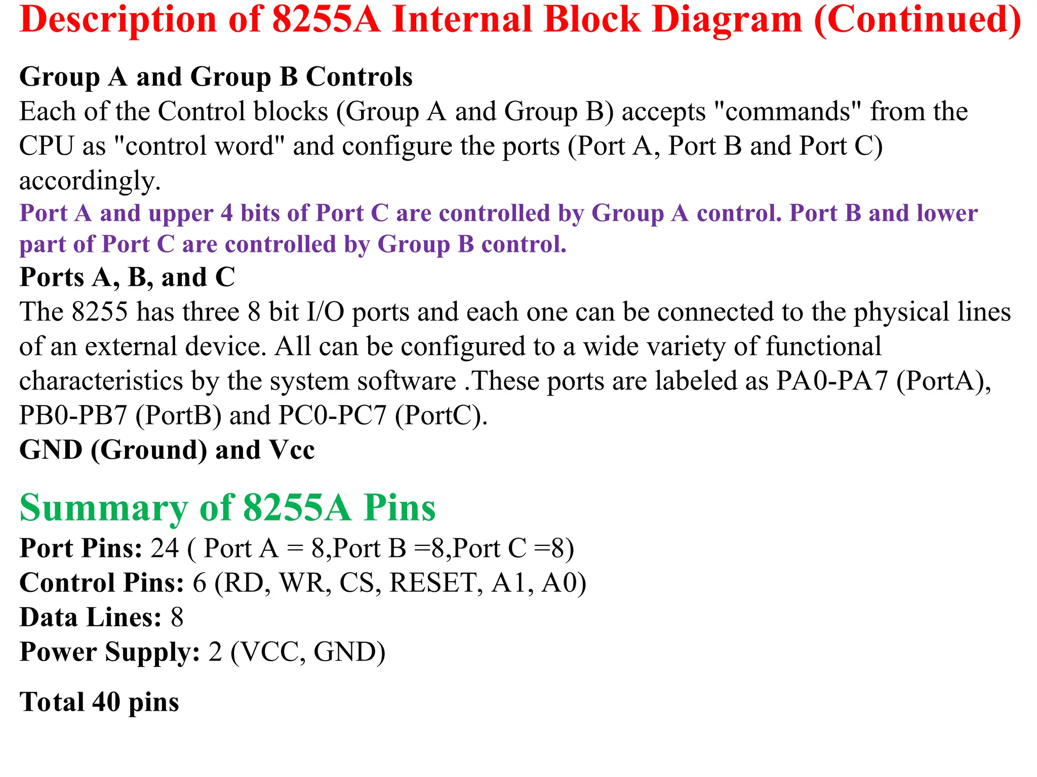
Description of 8255AInternal Block Diagram (Continued)
Group A and Group B Controls
Each of the Control blocks (Group A and Group B) accepts "commands" from the
CPU as "control word" and configure the ports (Port A, Port B and Port C)
accordingly.
Port A and upper 4 bits of Port C are controlled by Group A control. Port B and lower
part of Port C are controlled by Group B control.
Ports A, B, and C
The 8255 has three 8 bit I/O ports and each one can be connected to the physical lines
of an external device. All can be configured to a wide variety of functional
characteristics by the system software .These ports are labeled as PA0-PA7 (PortA),
PB0-PB7 (PortB) and PC0-PC7 (PortC).
GND (Ground) and Vcc
Summary of 8255A Pins
Port Pins: 24 ( Port A = 8,Port B =8,Port C =8)
Control Pins: 6 (RD, WR, CS, RESET, A1, A0)
Data Lines: 8
Power Supply: 2 (VCC, GND)
Total 40 pins
9.
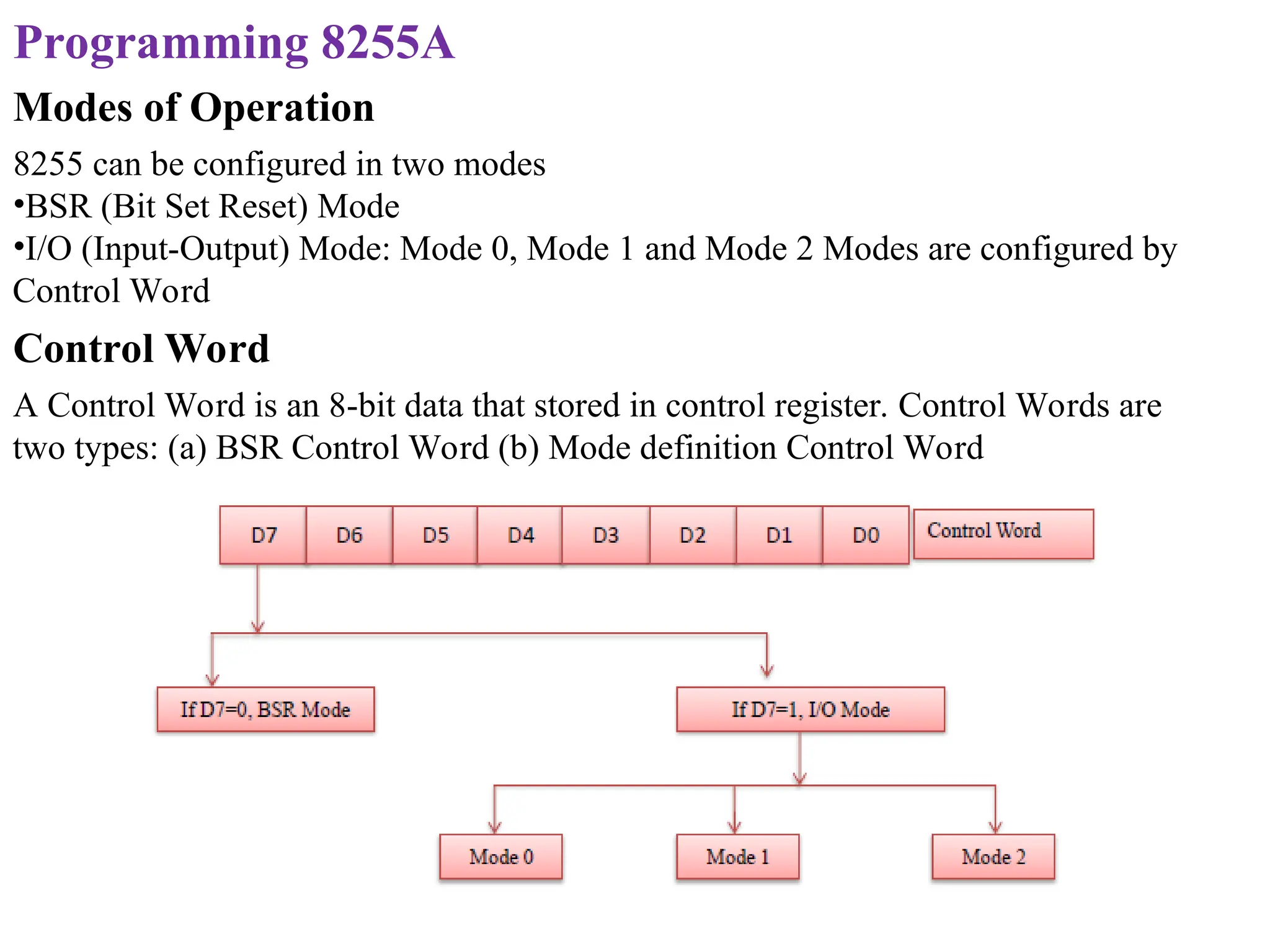
Programming 8255A
Modes ofOperation
8255 can be configured in two modes
•BSR (Bit Set Reset) Mode
•I/O (Input-Output) Mode: Mode 0, Mode 1 and Mode 2 Modes are configured by
Control Word
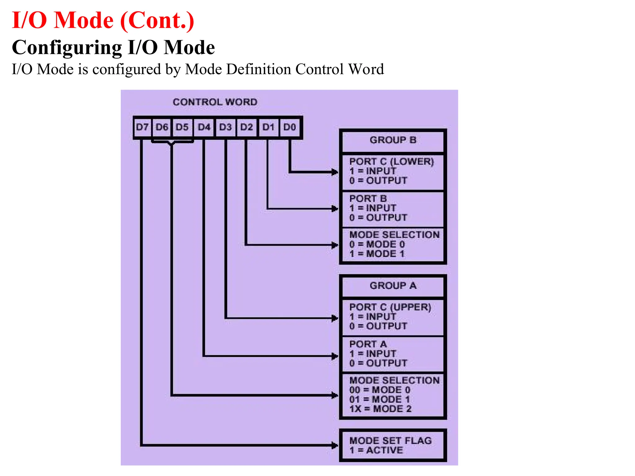
Control Word
A Control Word is an 8-bit data that stored in control register. Control Words are
two types: (a) BSR Control Word (b) Mode definition Control Word
10.
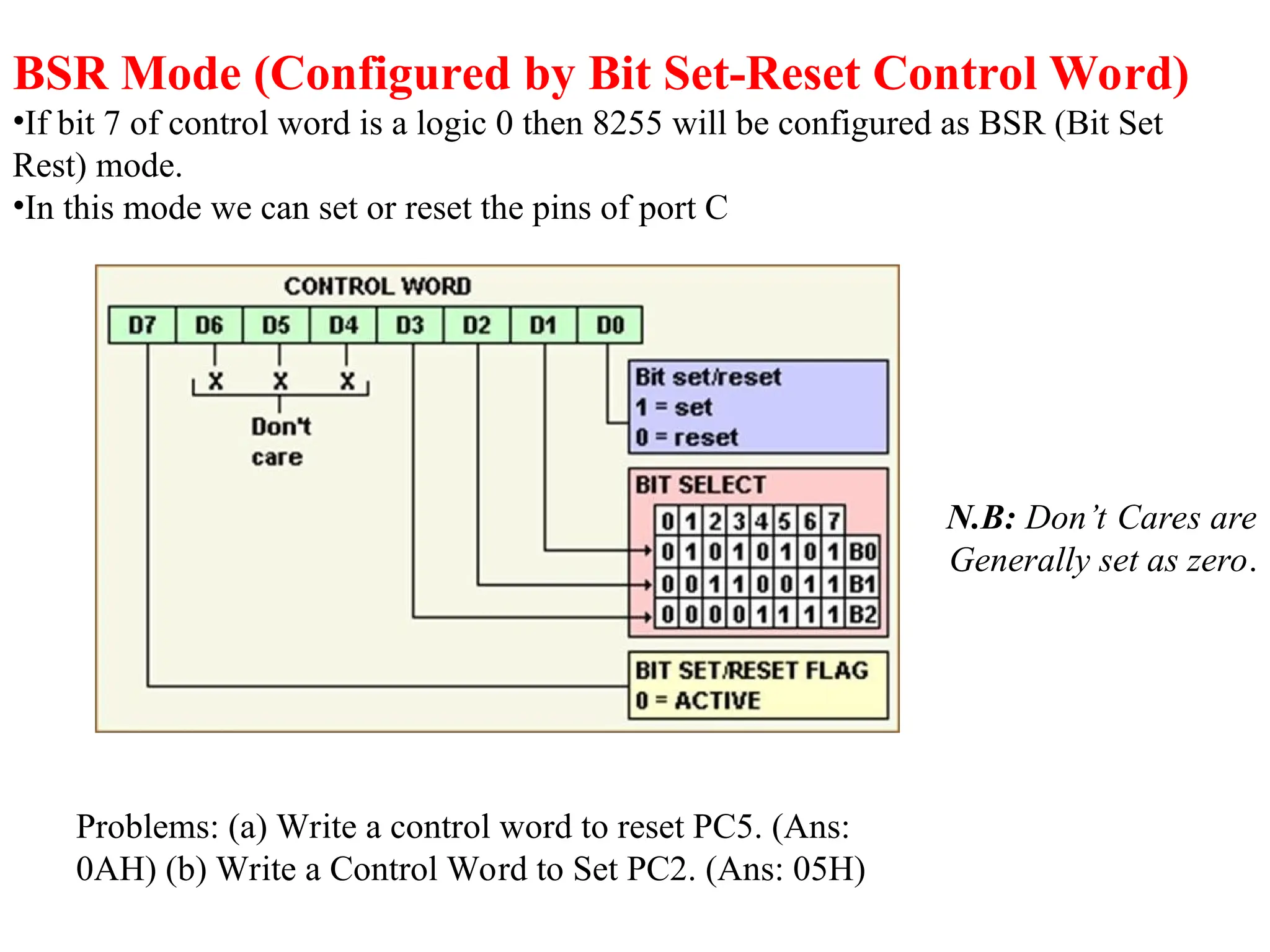
BSR Mode (Configuredby Bit Set-Reset Control Word)
•If bit 7 of control word is a logic 0 then 8255 will be configured as BSR (Bit Set
Rest) mode.
•In this mode we can set or reset the pins of port C
Problems: (a) Write a control word to reset PC5. (Ans:
0AH) (b) Write a Control Word to Set PC2. (Ans: 05H)
N.B: Don’t Cares are
Generally set as zero.
11.
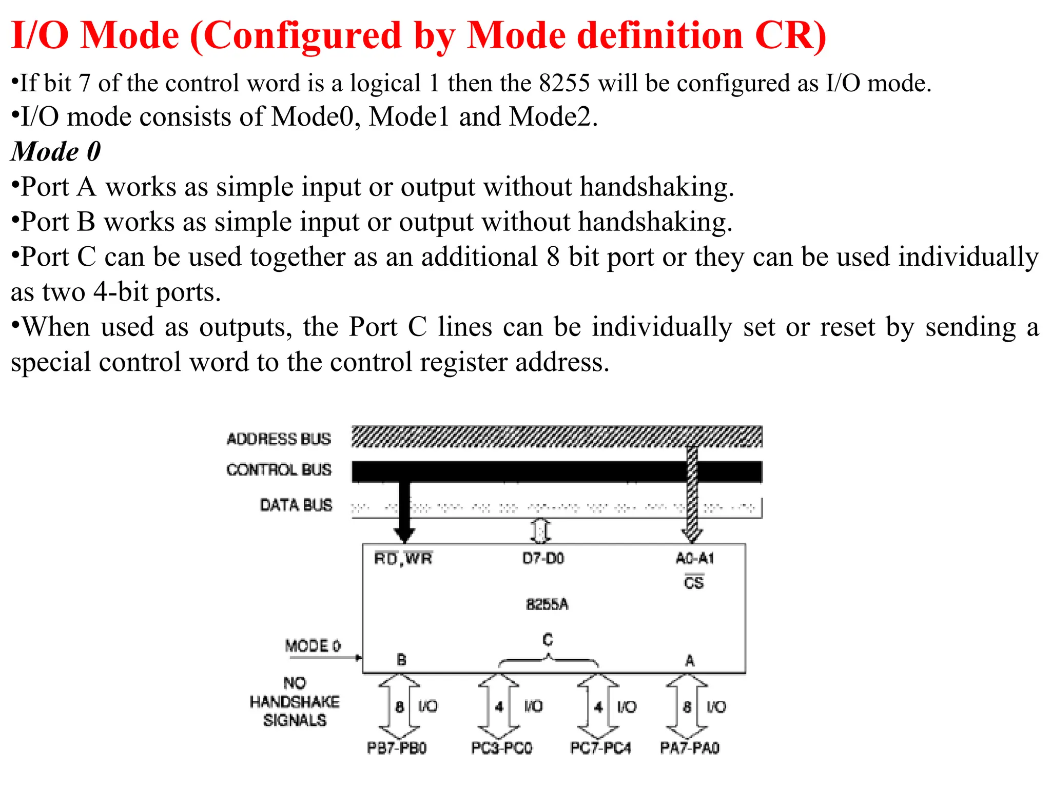
I/O Mode (Configuredby Mode definition CR)
•If bit 7 of the control word is a logical 1 then the 8255 will be configured as I/O mode.
•I/O mode consists of Mode0, Mode1 and Mode2.
Mode 0
•Port A works as simple input or output without handshaking.
•Port B works as simple input or output without handshaking.
•Port C can be used together as an additional 8 bit port or they can be used individually
as two 4-bit ports.
•When used as outputs, the Port C lines can be individually set or reset by sending a
special control word to the control register address.
12.
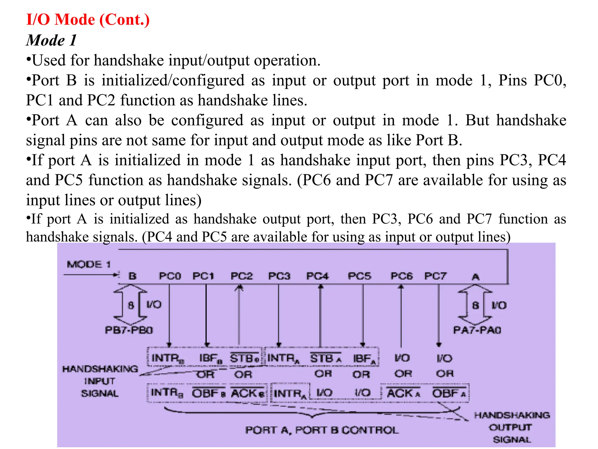
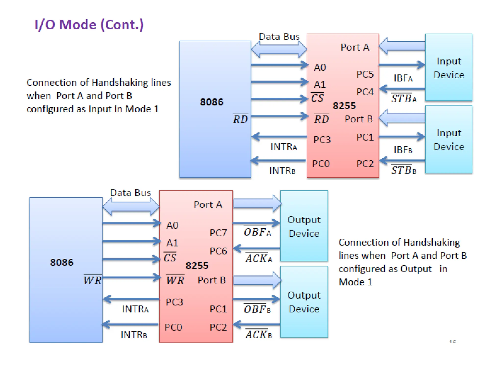
Mode 1
•Used forhandshake input/output operation.
•Port B is initialized/configured as input or output port in mode 1, Pins PC0,
PC1 and PC2 function as handshake lines.
•Port A can also be configured as input or output in mode 1. But handshake
signal pins are not same for input and output mode as like Port B.
•If port A is initialized in mode 1 as handshake input port, then pins PC3, PC4
and PC5 function as handshake signals. (PC6 and PC7 are available for using as
input lines or output lines)
•If port A is initialized as handshake output port, then PC3, PC6 and PC7 function as
handshake signals. (PC4 and PC5 are available for using as input or output lines)
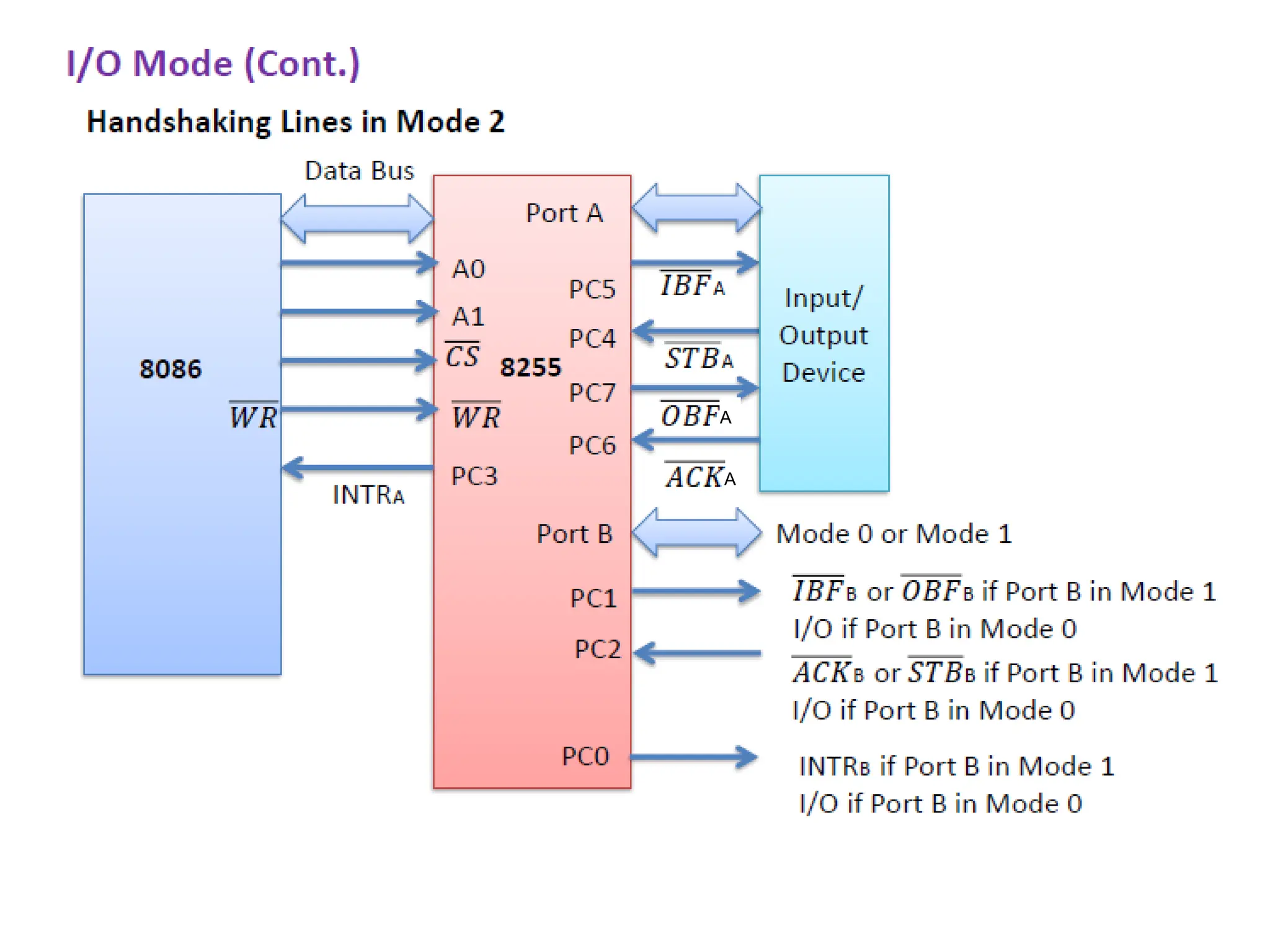
I/O Mode (Cont.)
14.
I/O Mode (Cont.)
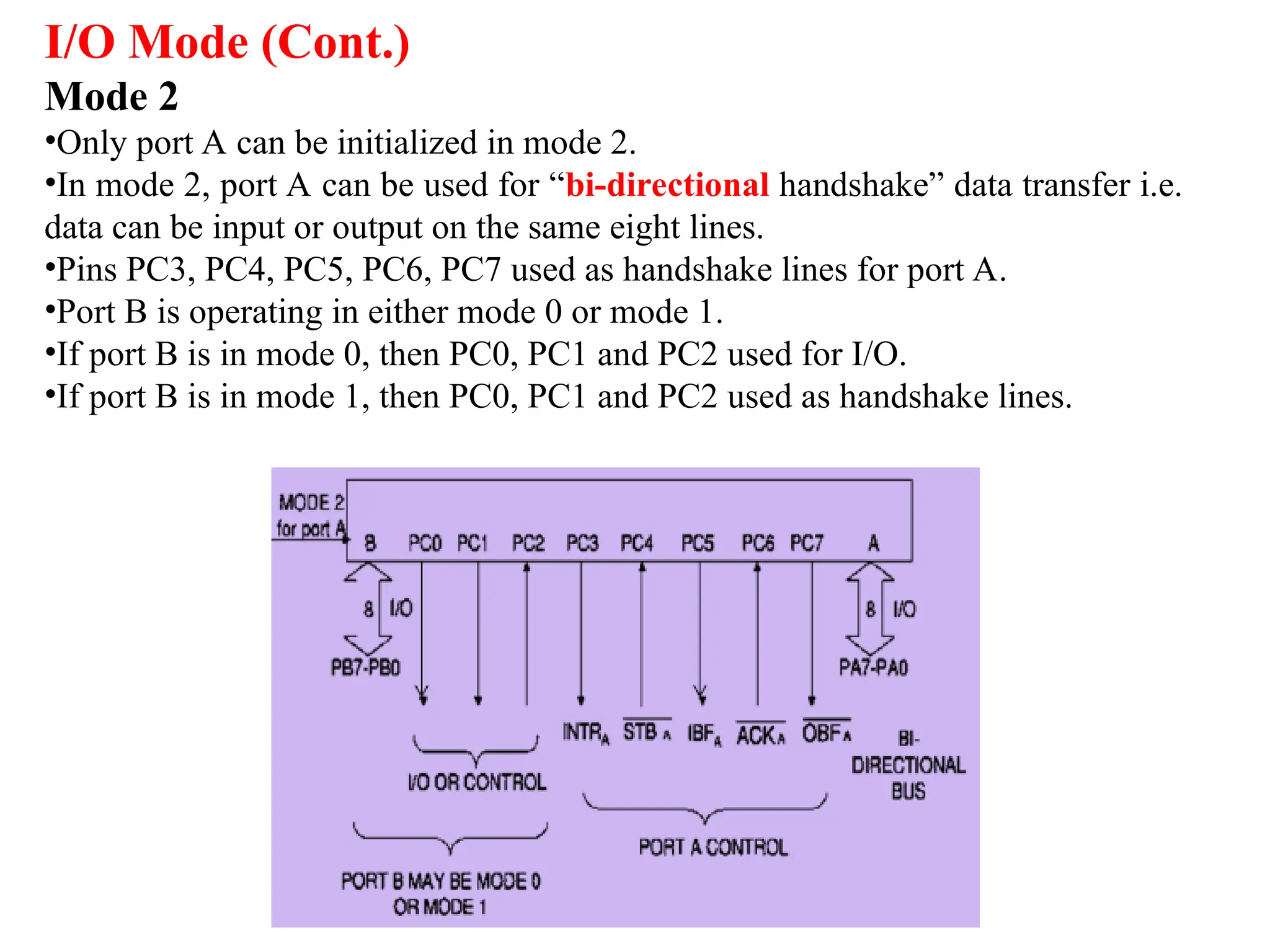
Mode2
•Only port A can be initialized in mode 2.
•In mode 2, port A can be used for “bi-directional handshake” data transfer i.e.
data can be input or output on the same eight lines.
•Pins PC3, PC4, PC5, PC6, PC7 used as handshake lines for port A.
•Port B is operating in either mode 0 or mode 1.
•If port B is in mode 0, then PC0, PC1 and PC2 used for I/O.
•If port B is in mode 1, then PC0, PC1 and PC2 used as handshake lines.
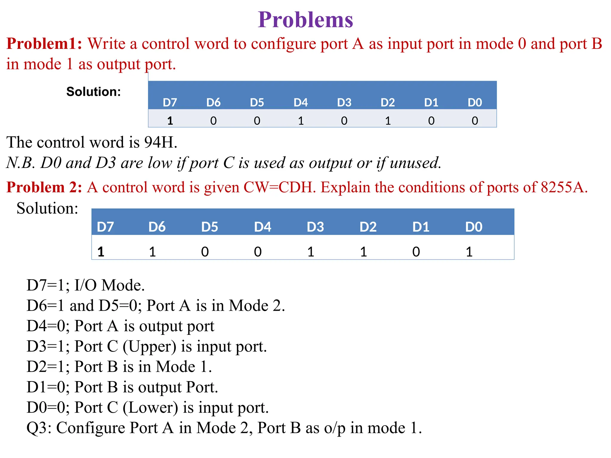
Problems
Problem1: Write acontrol word to configure port A as input port in mode 0 and port B
in mode 1 as output port.
Solution:
D7 D6 D5 D4 D3 D2 D1 D0
1 0 0 1 0 1 0 0
The control word is 94H.
N.B. D0 and D3 are low if port C is used as output or if unused.
Problem 2: A control word is given CW=CDH. Explain the conditions of ports of 8255A.
Solution:
D7 D6 D5 D4 D3 D2 D1 D0
1 1 0 0 1 1 0 1
D7=1; I/O Mode.
D6=1 and D5=0; Port A is in Mode 2.
D4=0; Port A is output port
D3=1; Port C (Upper) is input port.
D2=1; Port B is in Mode 1.
D1=0; Port B is output Port.
D0=0; Port C (Lower) is input port.
Q3: Configure Port A in Mode 2, Port B as o/p in mode 1.
18.
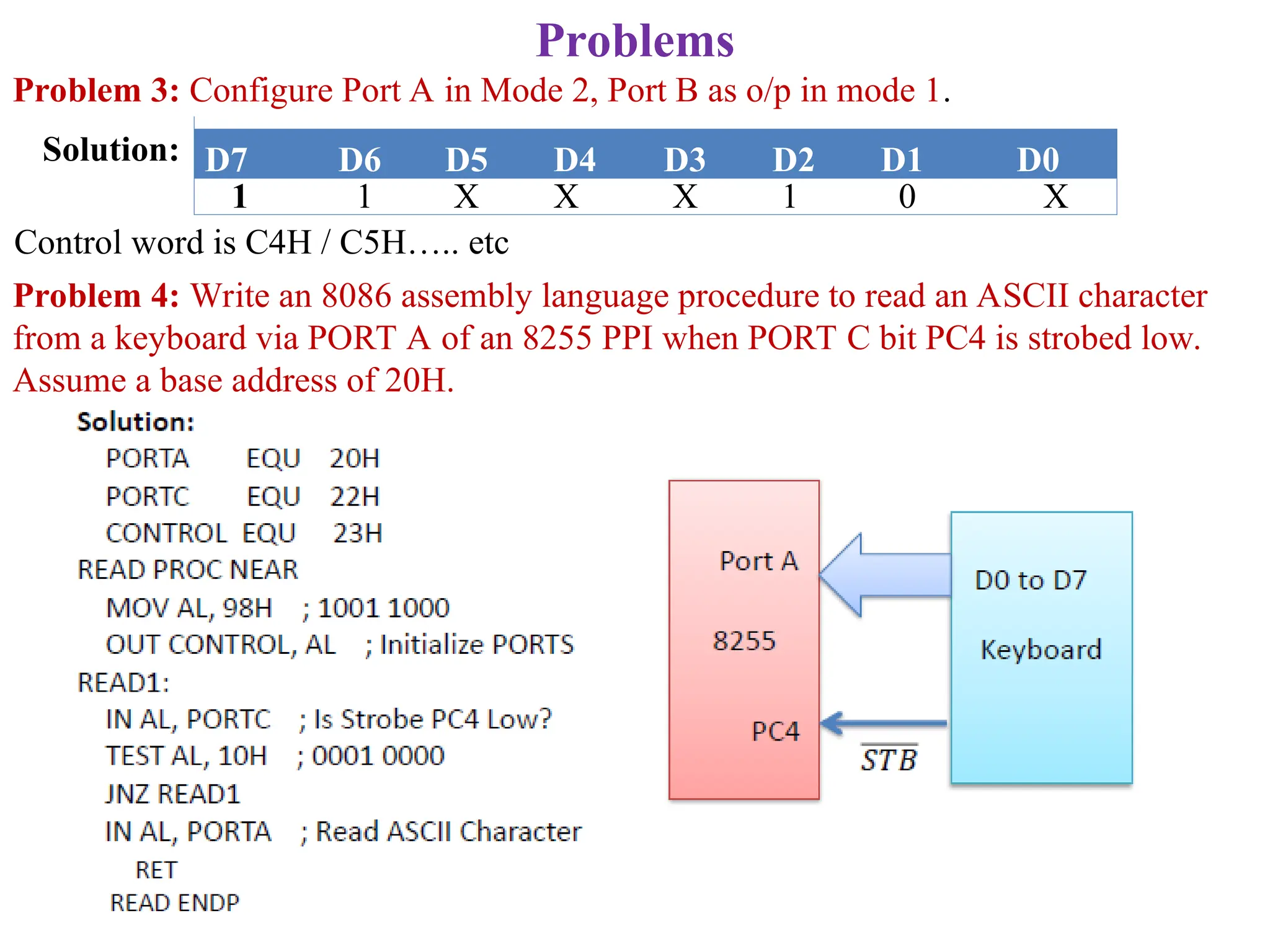
Problems
Problem 3: ConfigurePort A in Mode 2, Port B as o/p in mode 1.
Solution: D7 D6 D5 D4 D3 D2 D1 D0
1 1 X X X 1 0 X
Control word is C4H / C5H….. etc
Problem 4: Write an 8086 assembly language procedure to read an ASCII character
from a keyboard via PORT A of an 8255 PPI when PORT C bit PC4 is strobed low.
Assume a base address of 20H.
19.
Problem 04: ControlWord ber kora: D6 & D5 = 00 , karon kono mode er kotha bola nai
D4 = 1 jehetu port A ta input.
PC4 is storbed low: jokjoni question e storbed low eii type er kotha ullekh thakbe ,tokhon
j function ta kortesi oii pin ta k seta dhore nibo. Jemon 4 number problem e bole dise j
pc4 storbed low. PC4 holo upper 4 bit. Ar eii problem ta holo input neoar. Tai upper 4 bit
input.
Problem 5 holo output problem . PC0 storbed low. Tai lower 4 bit output dhore nibo. But
bolse after an active low acknowledge signal at pc5. Acknowledge signal ta holo 8255 er
jonno input. Tai upper 4 bit hobe input.
20.
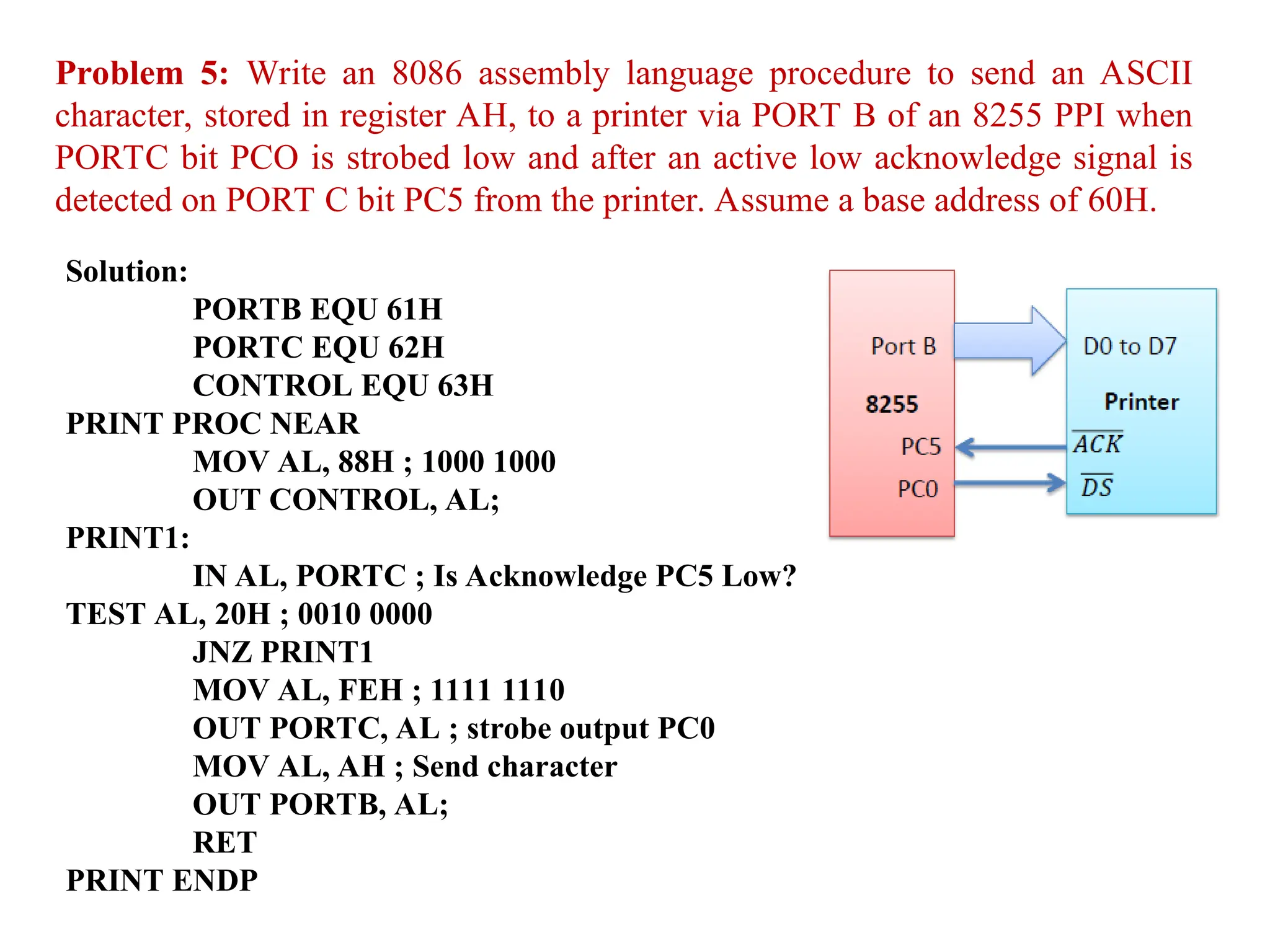
Problem 5: Writean 8086 assembly language procedure to send an ASCII
character, stored in register AH, to a printer via PORT B of an 8255 PPI when
PORTC bit PCO is strobed low and after an active low acknowledge signal is
detected on PORT C bit PC5 from the printer. Assume a base address of 60H.
Solution:
PORTB EQU 61H
PORTC EQU 62H
CONTROL EQU 63H
PRINT PROC NEAR
MOV AL, 88H ; 1000 1000
OUT CONTROL, AL;
PRINT1:
IN AL, PORTC ; Is Acknowledge PC5 Low?
TEST AL, 20H ; 0010 0000
JNZ PRINT1
MOV AL, FEH ; 1111 1110
OUT PORTC, AL ; strobe output PC0
MOV AL, AH ; Send character
OUT PORTB, AL;
RET
PRINT ENDP
21.
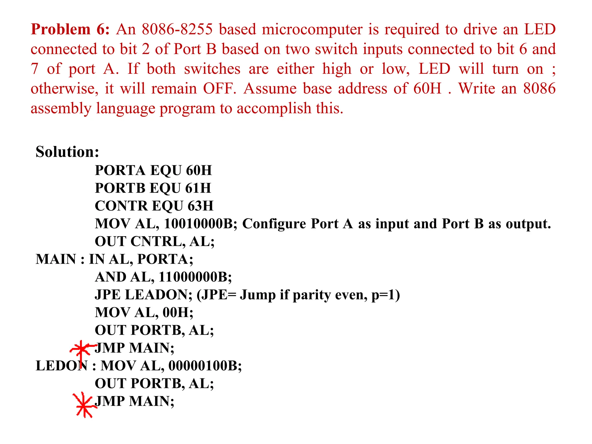
Problem 6: An8086-8255 based microcomputer is required to drive an LED
connected to bit 2 of Port B based on two switch inputs connected to bit 6 and
7 of port A. If both switches are either high or low, LED will turn on ;
otherwise, it will remain OFF. Assume base address of 60H . Write an 8086
assembly language program to accomplish this.
Solution:
PORTA EQU 60H
PORTB EQU 61H
CONTR EQU 63H
MOV AL, 10010000B; Configure Port A as input and Port B as output.
OUT CNTRL, AL;
MAIN : IN AL, PORTA;
AND AL, 11000000B;
JPE LEADON; (JPE= Jump if parity even, p=1)
MOV AL, 00H;
OUT PORTB, AL;
JMP MAIN;
LEDON : MOV AL, 00000100B;
OUT PORTB, AL;
JMP MAIN;
22.
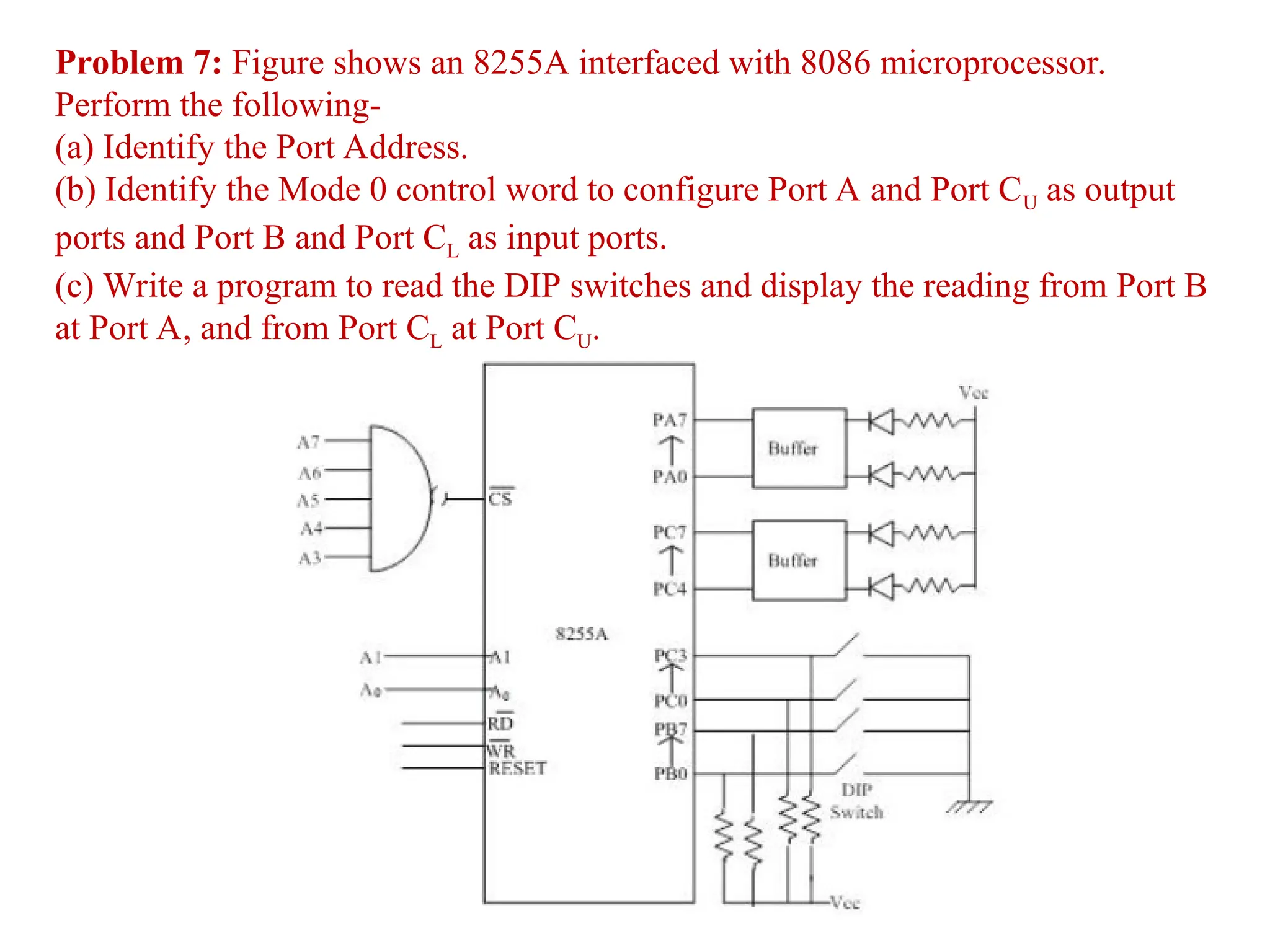
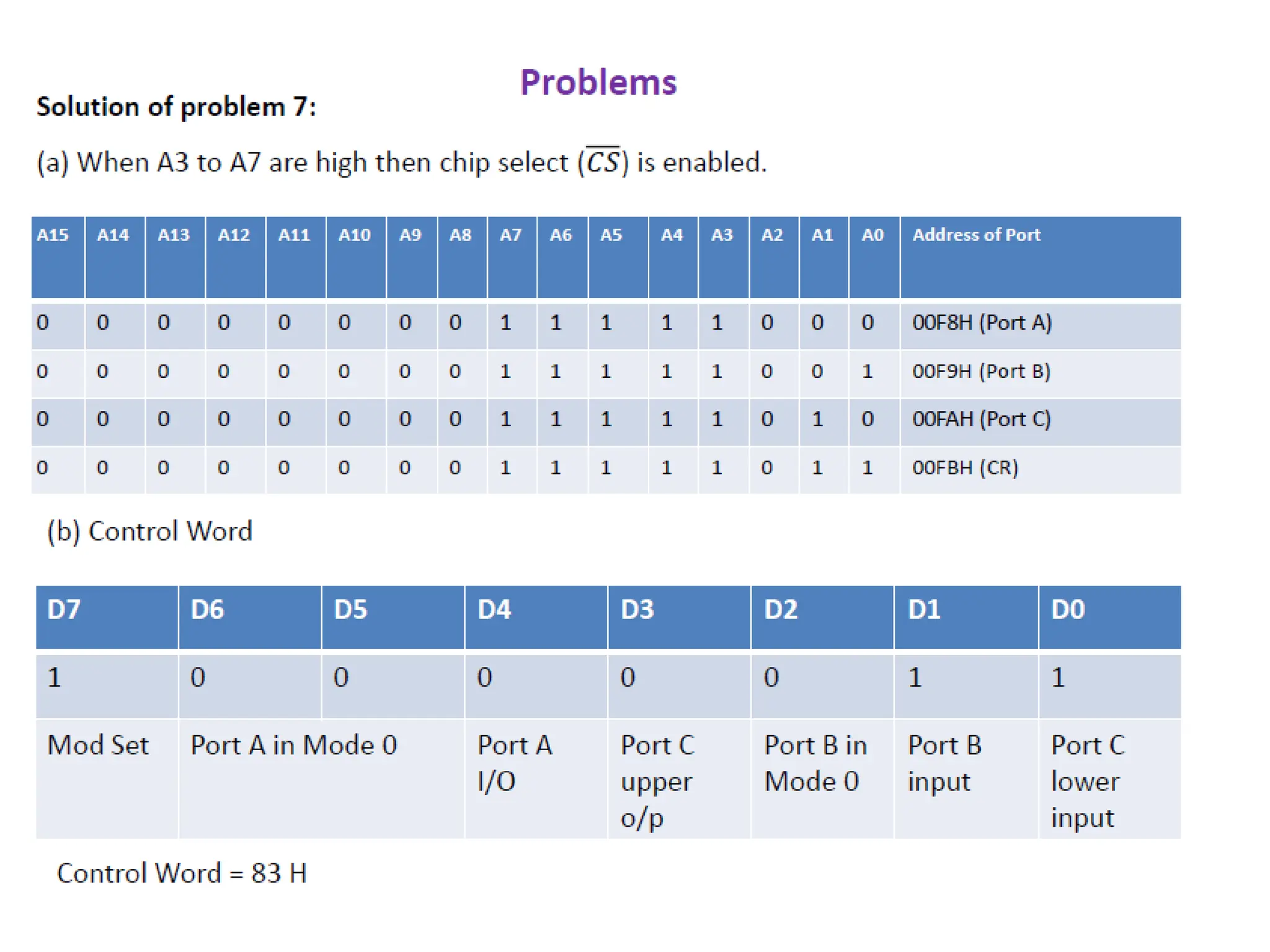
Problem 7: Figureshows an 8255A interfaced with 8086 microprocessor.
Perform the following-
(a) Identify the Port Address.
(b) Identify the Mode 0 control word to configure Port A and Port CU as output
ports and Port B and Port CL as input ports.
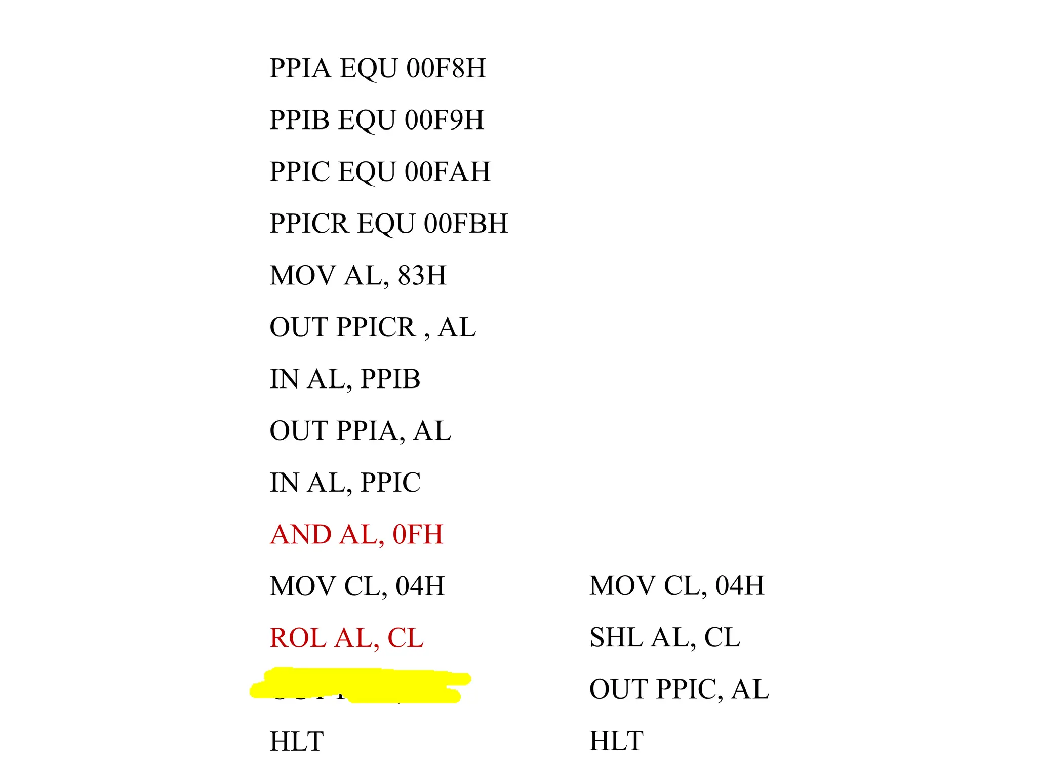
(c) Write a program to read the DIP switches and display the reading from Port B
at Port A, and from Port CL at Port CU.
24.
PPIA EQU 00F8H
PPIBEQU 00F9H
PPIC EQU 00FAH
PPICR EQU 00FBH
MOV AL, 83H
OUT PPICR , AL
IN AL, PPIB
OUT PPIA, AL
IN AL, PPIC
AND AL, 0FH
MOV CL, 04H
ROL AL, CL
OUT PPIC, AL
HLT
MOV CL, 04H
SHL AL, CL
OUT PPIC, AL
HLT
25.
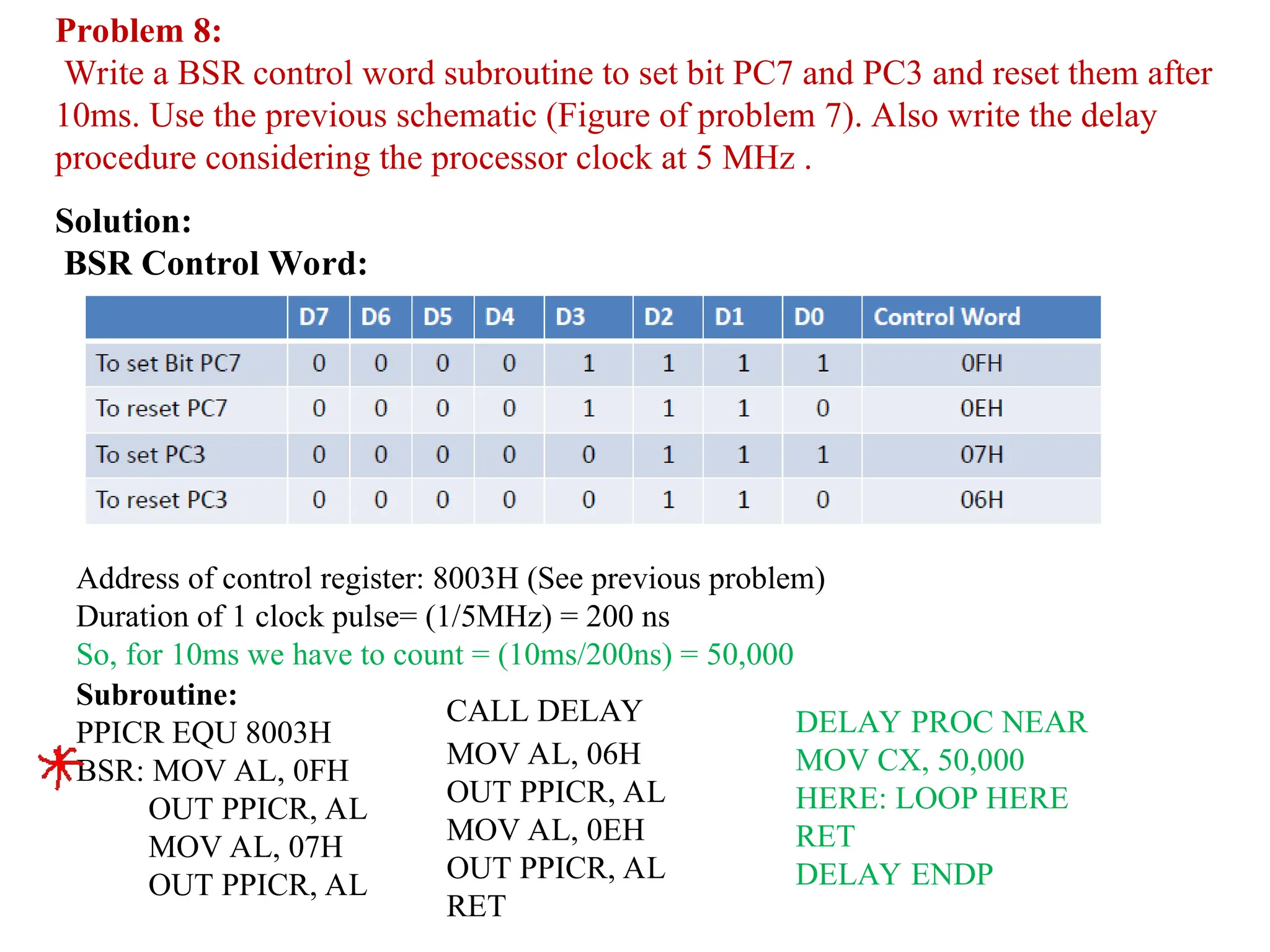
Problem 8:
Write aBSR control word subroutine to set bit PC7 and PC3 and reset them after
10ms. Use the previous schematic (Figure of problem 7). Also write the delay
procedure considering the processor clock at 5 MHz .
Solution:
BSR Control Word:
Subroutine:
PPICR EQU 8003H
BSR: MOV AL, 0FH
OUT PPICR, AL
MOV AL, 07H
OUT PPICR, AL
CALL DELAY DELAY PROC NEAR
MOV CX, 50,000
HERE: LOOP HERE
RET
DELAY ENDP
Address of control register: 8003H (See previous problem)
Duration of 1 clock pulse= (1/5MHz) = 200 ns
So, for 10ms we have to count = (10ms/200ns) = 50,000
MOV AL, 06H
OUT PPICR, AL
MOV AL, 0EH
OUT PPICR, AL
RET
26.
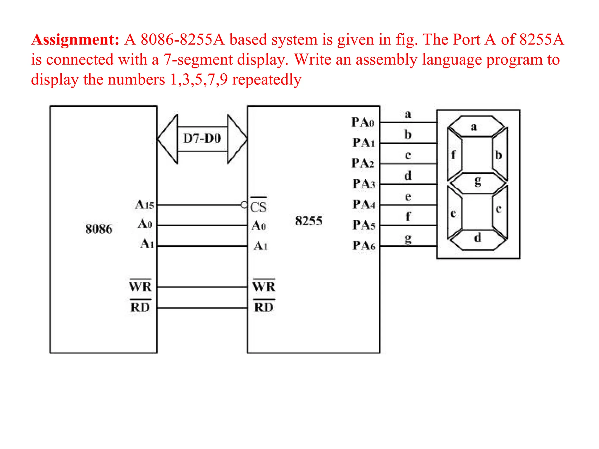
Assignment: A 8086-8255Abased system is given in fig. The Port A of 8255A
is connected with a 7-segment display. Write an assembly language program to
display the numbers 1,3,5,7,9 repeatedly
27.
Address of portA : 1000000000000000=8000H
Address of port B: 1000000000000001=8001H
Address of port C=8002H
Address of control register = 8003H
Program:
PORTA EQU 8000H
PORTB EQU 8001H
PORTC EQU 8002H
PPICR EQU 8003H
MOV AL, 10000000B
OUT PPICR, AL
L1: MOV SI, OFFSET DATA
L2: MOV AL, BYTE PTR CS:[SI]
CMP AL, 00H
JE L1
OUT PORTA, AL
CALL TIMER
INC SI
JMP L2
DATA: DB 00000110B
DB 01001111B
DB 01101101B
DB 00000111B
DB 01101111B
DB 00000000B
INT 3
TIMER: MOV CX,0
TIMER1: NOP
NOP
NOP
NOP
LOOP TIMER1
RET
![Address of port A : 1000000000000000=8000H
Address of port B: 1000000000000001=8001H
Address of port C=8002H
Address of control register = 8003H
Program:
PORTA EQU 8000H
PORTB EQU 8001H
PORTC EQU 8002H
PPICR EQU 8003H
MOV AL, 10000000B
OUT PPICR, AL
L1: MOV SI, OFFSET DATA
L2: MOV AL, BYTE PTR CS:[SI]
CMP AL, 00H
JE L1
OUT PORTA, AL
CALL TIMER
INC SI
JMP L2
DATA: DB 00000110B
DB 01001111B
DB 01101101B
DB 00000111B
DB 01101111B
DB 00000000B
INT 3
TIMER: MOV CX,0
TIMER1: NOP
NOP
NOP
NOP
LOOP TIMER1
RET](https://image.slidesharecdn.com/lecture8255modifiedbyme24-11-2020-250719152742-471fbd10/75/Lecture_8255_MODIfggggggggggggFIED_BY_ME_24-11-2020-ppt-27-2048.jpg)