MICROPROCESSOR 8085
LECTURE 23
I/O INTERFACING-II
PROF. SANDIP DAS
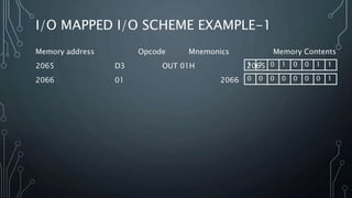
Memory address Opcode Mnemonics Memory Contents
2065 D3 OUT 01H 2065
2066 01 2066
I/O MAPPED I/O SCHEME EXAMPLE-1
1 1 0 1 0 0 1 1
0 0 0 0 0 0 0 1
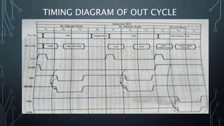
TIMING DIAGRAM OF OUT CYCLE
• Suppose, we want to display the LEDs connecting in output port
as per the combination of accumulator content.
• During the M3 cycle of the OUT instruction the processor places
the accumulator content on the data bus.
• The data bus is connected to a latch, so that we can catch the
information and display it via LEDs.
The Question now arises-
• when the latch will be enabled?
• what should be the address of that latch?
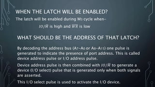
WHEN THE LATCH WILL BE ENABLED?
The latch will be enabled during M3 cycle when-
𝐼𝑂/ 𝑀 is high and 𝑊𝑅 is low
WHAT SHOULD BE THE ADDRESS OF THAT LATCH?
By decoding the address bus (A7-A0 or A8-A15) one pulse is
generated to indicate the presence of port address. This is called
device address pulse or I/O address pulse.
Device address pulse is then combined with 𝐼𝑂/ 𝑀 to generate a
device (I/O select) pulse that is generated only when both signals
are asserted.
This I/O select pulse is used to activate the I/O device.
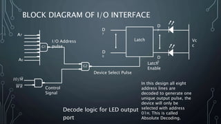
BLOCK DIAGRAM OF I/O INTERFACE
Decode logic for LED output
port
A7
A0
G1
𝐼𝑂/ 𝑀
𝑊𝑅
Latch
D
0
D
7
Latch
Enable
G2
Control
Signal
D
0
D
7
Vc
c
Device Select Pulse
I/O Address
pulse
In this design all eight
address lines are
decoded to generate one
unique output pulse, the
device will only be
selected with address
01H. This is called
Absolute Decoding.
PARTIAL DECODING
A2
G1
A7
𝑊𝑅
𝐼𝑂/ 𝑀
Latch
D
0
D
7
D
7
Vc
c
Latch
Enable
Device Select Pulse
Address line A0 and A1 are not
connected and they replaced by
𝐼𝑂/ 𝑀
and 𝑊𝑅 signals. Because the address
lines A0 and A1 are at don’t care
logic level, they can be assumed to
be 0 or 1. Thus this ouput latch can
be enabled by the addresses 00H,

20. io interfacing ii

  • 1.
    MICROPROCESSOR 8085 LECTURE 23 I/OINTERFACING-II PROF. SANDIP DAS
  • 2.
    Memory address OpcodeMnemonics Memory Contents 2065 D3 OUT 01H 2065 2066 01 2066 I/O MAPPED I/O SCHEME EXAMPLE-1 1 1 0 1 0 0 1 1 0 0 0 0 0 0 0 1
  • 3.
  • 4.
    • Suppose, wewant to display the LEDs connecting in output port as per the combination of accumulator content. • During the M3 cycle of the OUT instruction the processor places the accumulator content on the data bus. • The data bus is connected to a latch, so that we can catch the information and display it via LEDs. The Question now arises- • when the latch will be enabled? • what should be the address of that latch?
  • 5.
    WHEN THE LATCHWILL BE ENABLED? The latch will be enabled during M3 cycle when- 𝐼𝑂/ 𝑀 is high and 𝑊𝑅 is low WHAT SHOULD BE THE ADDRESS OF THAT LATCH? By decoding the address bus (A7-A0 or A8-A15) one pulse is generated to indicate the presence of port address. This is called device address pulse or I/O address pulse. Device address pulse is then combined with 𝐼𝑂/ 𝑀 to generate a device (I/O select) pulse that is generated only when both signals are asserted. This I/O select pulse is used to activate the I/O device.
  • 6.
    BLOCK DIAGRAM OFI/O INTERFACE Decode logic for LED output port A7 A0 G1 𝐼𝑂/ 𝑀 𝑊𝑅 Latch D 0 D 7 Latch Enable G2 Control Signal D 0 D 7 Vc c Device Select Pulse I/O Address pulse In this design all eight address lines are decoded to generate one unique output pulse, the device will only be selected with address 01H. This is called Absolute Decoding.
  • 7.
    PARTIAL DECODING A2 G1 A7 𝑊𝑅 𝐼𝑂/ 𝑀 Latch D 0 D 7 D 7 Vc c Latch Enable DeviceSelect Pulse Address line A0 and A1 are not connected and they replaced by 𝐼𝑂/ 𝑀 and 𝑊𝑅 signals. Because the address lines A0 and A1 are at don’t care logic level, they can be assumed to be 0 or 1. Thus this ouput latch can be enabled by the addresses 00H,