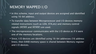
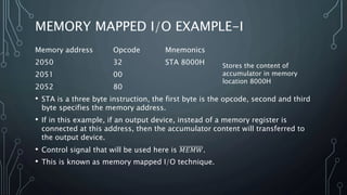
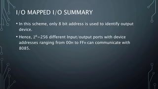
MICROPROCESSOR 8085
LECTURE 22
I/O INTERFACING-I
PROF. SANDIP DAS
TYPES OF I/O SCHEME
• Memory mapped I/O
• I/O mapped I/O (Peripheral mapped I/O)
MEMORY MAPPED I/O
• In this scheme, input and output devices are assigned and identified
using 16-bit address.
• To transfer data between Microprocessor and I/O devices memory
related instructions (such as LDA, STA,etc) and memory control
signals (𝑀𝐸𝑀𝑅 and 𝑀𝐸𝑀𝑊) are used.
• The microprocessor communicates with the I/O device as if it were
one of the memory locations.
• Since, I/O devices are identified using 16-bit addresses (16 address
lines), then 64KB memory space is shared between Memory register
and I/O devices.
MEMORY MAPPED I/O EXAMPLE-I
Memory address Opcode Mnemonics
2050 32 STA 8000H
2051 00
2052 80
• STA is a three byte instruction, the first byte is the opcode, second and third
byte specifies the memory address.
• If in this example, if an output device, instead of a memory register is
connected at this address, then the accumulator content will transferred to
the output device.
• Control signal that will be used here is 𝑀𝐸𝑀𝑊.
• This is known as memory mapped I/O technique.
Stores the content of
accumulator in memory
location 8000H
MEMORY MAPPED I/O EXAMPLE-II
Memory address Opcode Mnemonics
2050 3A LDA 8000H
2051 00
2052 80
• LDA is a three byte instruction, the first byte is the opcode, second
and third byte specifies the memory address.
• If in this example, if an output device, instead of a memory register is
connected at this address, then the content of I/O device will be
transferred to the accumulator.
• Control signal that will be used here is 𝑀𝐸𝑀𝑅.
Load the content of memory
location 8000H in Accumulator
I/O MAPPED I/O SCHEME
• In this scheme, the instructions IN or OUT are used for data
transfer between Microprocessor and I/O device.
• The I/O device, in this scheme, is identified using 8-bit
address.
• The instruction IN (opcode DB) inputs data from an input device
(such as a keyboard) into the accumulator.
• The instruction OUT (opcode D3) sends the contents of the
accumulator to an output device such as an LED display.
• These are 2-byte instructions, with second byte specifying the
address or the port number of an I/O device.
Memory address Opcode Mnemonics MEMORY CONTENTS
2065 DB IN 84H 2065
2066 84 2066
• When the above instruction is executed, it will first read the opcode stored
at location 2065H and 2066H.
• 2066H gives the port address 84H. From this I/O device (switch, keyboards,
Leds etc) the data bytes will be placed in the accumulator.
• Control signal 𝐼𝑂𝑅 enables the input port and the data from the input port
are placed on the data bus and transferred to the accumulator.
I/O MAPPED I/O SCHEME EXAMPLE-1
1 1 0 1 1 0 1 1
1 0 0 0 0 1 0 0
Memory address Opcode Mnemonics MEMORY
CONTENTS
2065 D3 OUT 01H 2065
2066 01 2066
• When the above instruction is executed, it will first read the opcode stored at location
2065H and 2066H.
• 2066H gives the port address 01H. Thus, this instruction transfers data from the
accumulator to the output device.
• Control signal 𝐼𝑂𝑊 enables the output port and the data from the accumulator are
transferred to the output device.
• If output port with the address 01H is designed as an LED display, then content of
accumulator is displayed in the LED display.
I/O MAPPED I/O SCHEME EXAMPLE-2
1 1 0 1 0 0 1 1
0 0 0 0 0 0 0 1
I/O MAPPED I/O SUMMARY
• In this scheme, only 8 bit address is used to identify output
device.
• Hence, 28
=256 different Input/output ports with device
addresses ranging from 00H to FFH can communicate with
8085.

19. io interfacing i

  • 1.
    MICROPROCESSOR 8085 LECTURE 22 I/OINTERFACING-I PROF. SANDIP DAS
  • 2.
    TYPES OF I/OSCHEME • Memory mapped I/O • I/O mapped I/O (Peripheral mapped I/O)
  • 3.
    MEMORY MAPPED I/O •In this scheme, input and output devices are assigned and identified using 16-bit address. • To transfer data between Microprocessor and I/O devices memory related instructions (such as LDA, STA,etc) and memory control signals (𝑀𝐸𝑀𝑅 and 𝑀𝐸𝑀𝑊) are used. • The microprocessor communicates with the I/O device as if it were one of the memory locations. • Since, I/O devices are identified using 16-bit addresses (16 address lines), then 64KB memory space is shared between Memory register and I/O devices.
  • 4.
    MEMORY MAPPED I/OEXAMPLE-I Memory address Opcode Mnemonics 2050 32 STA 8000H 2051 00 2052 80 • STA is a three byte instruction, the first byte is the opcode, second and third byte specifies the memory address. • If in this example, if an output device, instead of a memory register is connected at this address, then the accumulator content will transferred to the output device. • Control signal that will be used here is 𝑀𝐸𝑀𝑊. • This is known as memory mapped I/O technique. Stores the content of accumulator in memory location 8000H
  • 5.
    MEMORY MAPPED I/OEXAMPLE-II Memory address Opcode Mnemonics 2050 3A LDA 8000H 2051 00 2052 80 • LDA is a three byte instruction, the first byte is the opcode, second and third byte specifies the memory address. • If in this example, if an output device, instead of a memory register is connected at this address, then the content of I/O device will be transferred to the accumulator. • Control signal that will be used here is 𝑀𝐸𝑀𝑅. Load the content of memory location 8000H in Accumulator
  • 6.
    I/O MAPPED I/OSCHEME • In this scheme, the instructions IN or OUT are used for data transfer between Microprocessor and I/O device. • The I/O device, in this scheme, is identified using 8-bit address. • The instruction IN (opcode DB) inputs data from an input device (such as a keyboard) into the accumulator. • The instruction OUT (opcode D3) sends the contents of the accumulator to an output device such as an LED display. • These are 2-byte instructions, with second byte specifying the address or the port number of an I/O device.
  • 7.
    Memory address OpcodeMnemonics MEMORY CONTENTS 2065 DB IN 84H 2065 2066 84 2066 • When the above instruction is executed, it will first read the opcode stored at location 2065H and 2066H. • 2066H gives the port address 84H. From this I/O device (switch, keyboards, Leds etc) the data bytes will be placed in the accumulator. • Control signal 𝐼𝑂𝑅 enables the input port and the data from the input port are placed on the data bus and transferred to the accumulator. I/O MAPPED I/O SCHEME EXAMPLE-1 1 1 0 1 1 0 1 1 1 0 0 0 0 1 0 0
  • 8.
    Memory address OpcodeMnemonics MEMORY CONTENTS 2065 D3 OUT 01H 2065 2066 01 2066 • When the above instruction is executed, it will first read the opcode stored at location 2065H and 2066H. • 2066H gives the port address 01H. Thus, this instruction transfers data from the accumulator to the output device. • Control signal 𝐼𝑂𝑊 enables the output port and the data from the accumulator are transferred to the output device. • If output port with the address 01H is designed as an LED display, then content of accumulator is displayed in the LED display. I/O MAPPED I/O SCHEME EXAMPLE-2 1 1 0 1 0 0 1 1 0 0 0 0 0 0 0 1
  • 9.
    I/O MAPPED I/OSUMMARY • In this scheme, only 8 bit address is used to identify output device. • Hence, 28 =256 different Input/output ports with device addresses ranging from 00H to FFH can communicate with 8085.