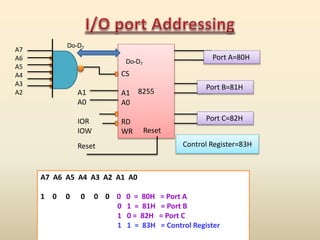
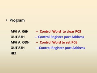
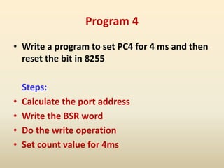
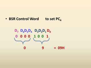
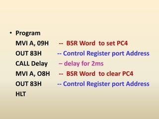
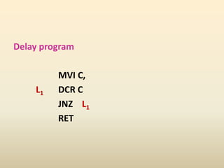
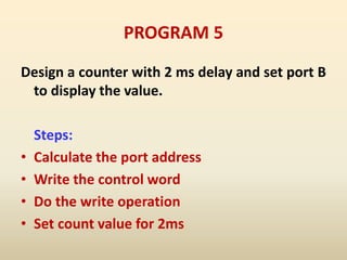
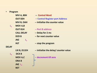
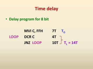
This document discusses programming the 8255 programmable peripheral interface chip. It provides 5 programs with steps to interface keys and displays, read inputs and write outputs, and set and clear bits on Port C. It explains calculating port addresses, initializing control words, and using read and write instructions. It also describes using a delay loop subroutine and calculating time delays for milliseconds. The document reviews important concepts and asks additional practice questions.


![• Time Delay (Td) = [To +(TL *N10)-3]T
= [ 7 +(14 *255)-3] 0.5 *10-6
= 1792µsec](https://image.slidesharecdn.com/8255programming-200408150734/85/8255-programming-29-320.jpg)
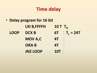
![• Time Delay (Td) = [To +(TL *N10)-3]T
= [ 10 +(24 *65535)-3] 0.5 *10-6
= 78642µsec](https://image.slidesharecdn.com/8255programming-200408150734/85/8255-programming-31-320.jpg)
![• Time delay for 2ms
Time Delay (Td) = [To +(TL *N10)-3]T
2ms = [ 10+(24 *N10) -3]*0.5* 10-6
N10 = 2 * 10-3 -20 +3
0.5* 10-6 24
= 165 = A5H](https://image.slidesharecdn.com/8255programming-200408150734/85/8255-programming-32-320.jpg)
![• Time delay for 3ms
Time Delay (Td) = [To +(TL *N10)-3]T
3ms = [ 10+(24 *N10) -3]*0.5* 10-6
N10 = 3 * 10-3 -10 +3
0.5* 10-6 24
= 249 = F9H](https://image.slidesharecdn.com/8255programming-200408150734/85/8255-programming-33-320.jpg)
![• Time delay for 2ms
Time Delay (Td) = [To +(TL *N10)-3]T
2ms = [ 7+(14 *N10) -3]*0.5* 10-6
N10 = 2 * 10-3 -7 +3
0.5* 10-6 14
= 165 = A5H](https://image.slidesharecdn.com/8255programming-200408150734/85/8255-programming-34-320.jpg)