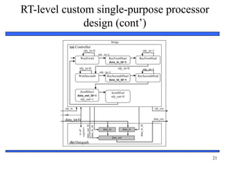
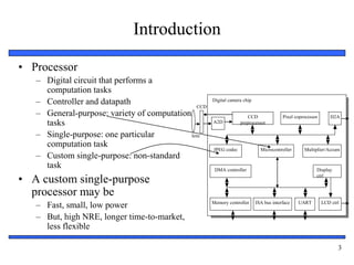
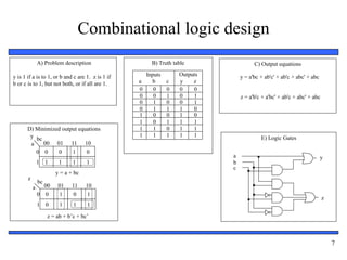
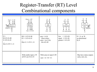
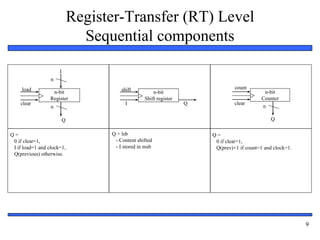
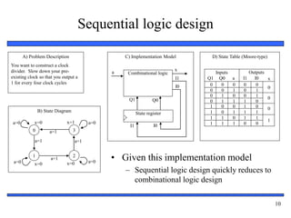
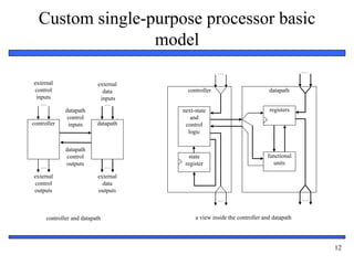
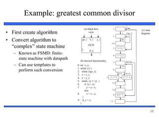
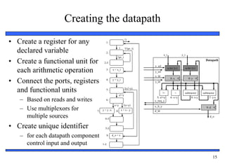
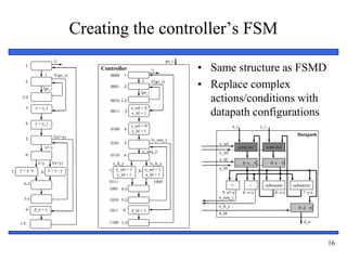
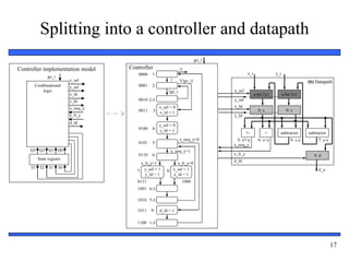
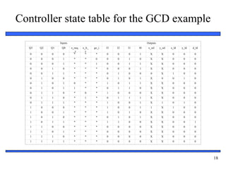
3. 3
Introduction
• Processor
– Digital circuit that performs a
computation tasks
– Controller and datapath
– General-purpose: variety of computation
tasks
– Single-purpose: one particular
computation task
– Custom single-purpose: non-standard
task
• A custom single-purpose
processor may be
– Fast, small, low power
– But, high NRE, longer time-to-market,
less flexible
Microcontroller
CCD
preprocessor
Pixel coprocessor
A2D
D2A
JPEG codec
DMA controller
Memory controller ISA bus interface UART LCD ctrl
Display
ctrl
Multiplier/Accum
Digital camera chip
lens
CCD
4. 4
CMOS transistor on silicon
• Transistor
– The basic electrical component in digital systems
– Acts as an on/off switch
– Voltage at “gate” controls whether current flows from
source to drain
– Don’t confuse this “gate” with a logic gate
source drain
oxide
gate
IC package IC
channel
Silicon substrate
gate
source
drain
Conducts
if gate=1
1
5. 5
CMOS transistor implementations
• Complementary Metal Oxide
Semiconductor
• We refer to logic levels
– Typically 0 is 0V, 1 is 5V
• Two basic CMOS types
– nMOS conducts if gate=1
– pMOS conducts if gate=0
– Hence “complementary”
• Basic gates
– Inverter, NAND, NOR
x F = x'
1
inverter
0
F = (xy)'
x
1
x
y
y
NAND gate
0
1
F = (x+y)'
x y
x
y
NOR gate
0
gate
source
drain
nMOS
Conducts
if gate=1
gate
source
drain
pMOS
Conducts
if gate=0
6. 6
Basic logic gates
F = x y
AND
F = (x y)’
NAND
F = x y
XOR
F = x
Driver
F = x’
Inverter
x F
F = x + y
OR
F = (x+y)’
NOR
x F
x
y
F
F
x
y
x
y
F
x
y
F
x
y
F
F = x y
XNOR
F
y
x
x
0
y
0
F
0
0 1 0
1 0 0
1 1 1
x
0
y
0
F
0
0 1 1
1 0 1
1 1 1
x
0
y
0
F
0
0 1 1
1 0 1
1 1 0
x
0
y
0
F
1
0 1 0
1 0 0
1 1 1
x
0
y
0
F
1
0 1 1
1 0 1
1 1 0
x
0
y
0
F
1
0 1 0
1 0 0
1 1 0
x F
0 0
1 1
x F
0 1
1 0
7. 7
Combinational logic design
A) Problem description
y is 1 if a is to 1, or b and c are 1. z is 1 if
b or c is to 1, but not both, or if all are 1.
D) Minimized output equations
00
0
1
01 11 10
0
1
0 1 0
1 1 1
a
bc
y
y = a + bc
00
0
1
01 11 10
0
0
1 0 1
1 1 1
z
z = ab + b’c + bc’
a
bc
C) Output equations
y = a'bc + ab'c' + ab'c + abc' + abc
z = a'b'c + a'bc' + ab'c + abc' + abc
B) Truth table
1 0 1 1 1
1 1 0 1 1
1 1 1 1 1
0 0 1 0 1
0 1 0 0 1
0 1 1 1 0
1 0 0 1 0
0
0 0 0 0
Inputs
a b c
Outputs
y z
E) Logic Gates
a
b
c
y
z
8. 8
Register-Transfer (RT) Level
Combinational components
With enable input e
all O’s are 0 if e=0
With carry-in input Ci
sum = A + B + Ci
May have status outputs
carry, zero, etc.
O =
I0 if S=0..00
I1 if S=0..01
…
I(m-1) if S=1..11
O0 =1 if I=0..00
O1 =1 if I=0..01
…
O(n-1) =1 if I=1..11
sum = A+B
(first n bits)
carry = (n+1)’th
bit of A+B
less = 1 if A<B
equal =1 if A=B
greater=1 if A>B
O = A op B
op determined
by S.
n-bit, m x 1
Multiplexor
O
…
S0
S(log m)
n
n
I(m-1) I1 I0
…
log n x n
Decoder
…
O1 O0
O(n-1)
I0
I(log n -1)
…
n-bit
Adder
n
A B
n
sum
carry
n-bit
Comparator
n n
A B
less equal greater
n bit,
m function
ALU
n n
A B
…
S0
S(log m)
n
O
9. 9
Register-Transfer (RT) Level
Sequential components
Q =
0 if clear=1,
I if load=1 and clock=1,
Q(previous) otherwise.
Q =
0 if clear=1,
Q(prev)+1 if count=1 and clock=1.
clear
n-bit
Register
n
n
load
I
Q
shift
I Q
n-bit
Shift register
n-bit
Counter
n
Q
Q = lsb
- Content shifted
- I stored in msb
clear
count
10. 10
Sequential logic design
A) Problem Description
You want to construct a clock
divider. Slow down your pre-
existing clock so that you output a
1 for every four clock cycles
0
1 2
3
x=0
x=1
x=0
x=0
a=1 a=1
a=1
a=1
a=0
a=0
a=0
a=0
B) State Diagram
C) Implementation Model
Combinational logic
State register
a
x
I0
I0
I1
I1
Q1 Q0
D) State Table (Moore-type)
1 0 1 1 1
1 1 0 1 1
1 1 1 0 0
0 0 1 0 1
0 1 0 0 1
0 1 1 1 0
1 0 0 1 0
0
0 0 0 0
Inputs
Q1 Q0 a
Outputs
I1 I0
1
0
0
0
x
• Given this implementation model
– Sequential logic design quickly reduces to
combinational logic design
12. 12
Custom single-purpose processor basic
model
controller and datapath
controller datapath
…
…
external
control
inputs
external
control
outputs
…
external
data
inputs
…
external
data
outputs
datapath
control
inputs
datapath
control
outputs
… …
a view inside the controller and datapath
controller datapath
… …
state
register
next-state
and
control
logic
registers
functional
units
13. 13
Example: greatest common divisor
GCD
(a) black-box
view
x_i y_i
d_o
go_i
0: int x, y;
1: while (1) {
2: while (!go_i);
3: x = x_i;
4: y = y_i;
5: while (x != y) {
6: if (x < y)
7: y = y - x;
else
8: x = x - y;
}
9: d_o = x;
}
(b) desired functionality
y = y -x
7: x = x - y
8:
6-J:
x!=y
5: !(x!=y)
x<y !(x<y)
6:
5-J:
1:
1
!1
x = x_i
3:
y = y_i
4:
2:
2-J:
!go_i
!(!go_i)
d_o = x
1-J:
9:
(c) state
diagram
• First create algorithm
• Convert algorithm to
“complex” state machine
– Known as FSMD: finite-
state machine with datapath
– Can use templates to
perform such conversion
14. 14
State diagram templates
Assignment statement
a = b
next statement
a = b
next
statement
Loop statement
while (cond) {
loop-body-
statements
}
next statement
loop-body-
statements
cond
next
statement
!cond
J:
C:
Branch statement
if (c1)
c1 stmts
else if c2
c2 stmts
else
other stmts
next statement
c1
c2 stmts
!c1*c2 !c1*!c2
next
statement
others
c1 stmts
J:
C:
15. 15
Creating the datapath
• Create a register for any
declared variable
• Create a functional unit for
each arithmetic operation
• Connect the ports, registers
and functional units
– Based on reads and writes
– Use multiplexors for
multiple sources
• Create unique identifier
– for each datapath component
control input and output
y = y -x
7: x = x - y
8:
6-J:
x!=y
5: !(x!=y)
x<y !(x<y)
6:
5-J:
1:
1
!1
x = x_i
3:
y = y_i
4:
2:
2-J:
!go_i
!(!go_i)
d_o = x
1-J:
9:
subtractor subtractor
7: y-x
8: x-y
5: x!=y 6: x<y
x_i y_i
d_o
0: x 0: y
9: d
n-bit 2x1 n-bit 2x1
x_sel
y_sel
x_ld
y_ld
x_neq_y
x_lt_y
d_ld
<
5: x!=y
!=
Datapath
18. 18
Controller state table for the GCD example
Inputs Outputs
Q3 Q2 Q1 Q0 x_neq
_y
x_lt_
y
go_i I3 I2 I1 I0 x_sel y_sel x_ld y_ld d_ld
0 0 0 0 * * * 0 0 0 1 X X 0 0 0
0 0 0 1 * * 0 0 0 1 0 X X 0 0 0
0 0 0 1 * * 1 0 0 1 1 X X 0 0 0
0 0 1 0 * * * 0 0 0 1 X X 0 0 0
0 0 1 1 * * * 0 1 0 0 0 X 1 0 0
0 1 0 0 * * * 0 1 0 1 X 0 0 1 0
0 1 0 1 0 * * 1 0 1 1 X X 0 0 0
0 1 0 1 1 * * 0 1 1 0 X X 0 0 0
0 1 1 0 * 0 * 1 0 0 0 X X 0 0 0
0 1 1 0 * 1 * 0 1 1 1 X X 0 0 0
0 1 1 1 * * * 1 0 0 1 X 1 0 1 0
1 0 0 0 * * * 1 0 0 1 1 X 1 0 0
1 0 0 1 * * * 1 0 1 0 X X 0 0 0
1 0 1 0 * * * 0 1 0 1 X X 0 0 0
1 0 1 1 * * * 1 1 0 0 X X 0 0 1
1 1 0 0 * * * 0 0 0 0 X X 0 0 0
1 1 0 1 * * * 0 0 0 0 X X 0 0 0
1 1 1 0 * * * 0 0 0 0 X X 0 0 0
1 1 1 1 * * * 0 0 0 0 X X 0 0 0
19. 19
Completing the GCD custom single-purpose
processor design
• We finished the datapath
• We have a state table for
the next state and control
logic
– All that’s left is
combinational logic
design
• This is not an optimized
design, but we see the
basic steps
… …
a view inside the controller and datapath
controller datapath
… …
state
register
next-state
and
control
logic
registers
functional
units
20. 20
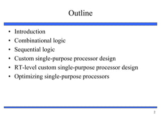
• We often start with a state
machine
– Rather than algorithm
– Cycle timing often too central
to functionality
• Example
– Bus bridge that converts 4-bit
bus to 8-bit bus
– Start with FSMD
– Known as register-transfer
(RT) level
– Exercise: complete the design
RT-level custom single-purpose processor
design
Problem
Specification
Bridge
A single-purpose processor that
converts two 4-bit inputs, arriving one
at a time over data_in along with a
rdy_in pulse, into one 8-bit output on
data_out along with a rdy_out pulse.
Sender
data_in(4)
rdy_in rdy_out
data_out(8)
Receiver
clock
FSMD
WaitFirst4 RecFirst4Start
data_lo=data_in
WaitSecond4
rdy_in=1
rdy_in=0
RecFirst4End
rdy_in=1
RecSecond4Start
data_hi=data_in
RecSecond4End
rdy_in=1
rdy_in=0
rdy_in=1
rdy_in=0
Send8Start
data_out=data_hi
& data_lo
rdy_out=1
Send8End
rdy_out=0
Bridge
rdy_in=0
Inputs
rdy_in: bit; data_in: bit[4];
Outputs
rdy_out: bit; data_out:bit[8]
Variables
data_lo, data_hi: bit[4];
22. 22
Optimizing single-purpose processors
• Optimization is the task of making design metric
values the best possible
• Optimization opportunities
– original program
– FSMD
– datapath
– FSM
23. 23
Optimizing the original program
• Analyze program attributes and look for areas of
possible improvement
– number of computations
– size of variable
– time and space complexity
– operations used
• multiplication and division very expensive
24. 24
Optimizing the original program (cont’)
0: int x, y;
1: while (1) {
2: while (!go_i);
3: x = x_i;
4: y = y_i;
5: while (x != y) {
6: if (x < y)
7: y = y - x;
else
8: x = x - y;
}
9: d_o = x;
}
0: int x, y, r;
1: while (1) {
2: while (!go_i);
// x must be the larger number
3: if (x_i >= y_i) {
4: x=x_i;
5: y=y_i;
}
6: else {
7: x=y_i;
8: y=x_i;
}
9: while (y != 0) {
10: r = x % y;
11: x = y;
12: y = r;
}
13: d_o = x;
}
original program optimized program
replace the subtraction
operation(s) with modulo
operation in order to speed
up program
GCD(42, 8) - 9 iterations to complete the loop
x and y values evaluated as follows : (42, 8), (34, 8),
(26,8), (18,8), (10, 8), (2,8), (2,6), (2,4), (2,2).
GCD(42,8) - 3 iterations to complete the loop
x and y values evaluated as follows: (42, 8), (8,2),
(2,0)
25. 25
Optimizing the FSMD
• Areas of possible improvements
– merge states
• states with constants on transitions can be eliminated, transition
taken is already known
• states with independent operations can be merged
– separate states
• states which require complex operations (a*b*c*d) can be broken
into smaller states to reduce hardware size
– scheduling
26. 26
Optimizing the FSMD (cont.)
int x, y;
7:
9:
2:
go_i !go_i
x = x_i
y = y_i
x<y x>y
y = y -x x = x - y
3:
5:
8:
d_o = x
7:
int x, y;
y = y -x x = x - y
8:
6-J:
x!=y
5: !(x!=y)
x<y !(x<y)
6:
5-J:
1:
1
!1
x = x_i
y = y_i
4:
2:
2-J:
!go_i
!(!go_i)
d_o = x
1-J:
9:
3:
original FSMD optimized FSMD
eliminate state 1 – transitions have constant values
merge state 2 and state 2J – no loop operation in
between them
merge state 3 and state 4 – assignment operations are
independent of one another
merge state 5 and state 6 – transitions from state 6 can
be done in state 5
eliminate state 5J and 6J – transitions from each state
can be done from state 7 and state 8, respectively
eliminate state 1-J – transition from state 1-J can be
done directly from state 9
27. 27
Optimizing the datapath
• Sharing of functional units
– one-to-one mapping, as done previously, is not necessary
– if same operation occurs in different states, they can share a
single functional unit
• Multi-functional units
– ALUs support a variety of operations, it can be shared
among operations occurring in different states
28. 28
Optimizing the FSM
• State encoding
– task of assigning a unique bit pattern to each state in an FSM
– size of state register and combinational logic vary
– can be treated as an ordering problem
• State minimization
– task of merging equivalent states into a single state
• Two states are equivalent if, for all possible input combinations the two
states generate the same outputs and transitions to the same next state.