Download to read offline


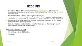
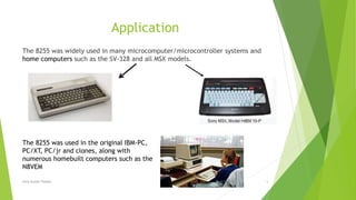


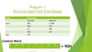
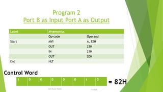


The document describes an experiment involving the Intel 8255 Programmable Peripheral Interface chip. It discusses: 1) The 8255 PPI chip's architecture which includes 3 8-bit I/O ports (A, B, C) that can be configured as input or output ports in different operating modes. 2) The two main operating modes - I/O mode and Bit Set/Reset mode. I/O mode has three sub-modes (Mode 0, 1, 2) for different handshake capabilities. 3) Examples of 8255 PPI applications in computers like the original IBM PC. 4) Example assembly language programs to configure the 8255 ports in different input/output modes