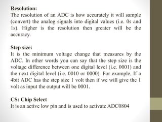
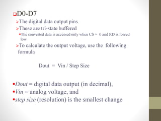
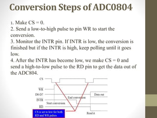
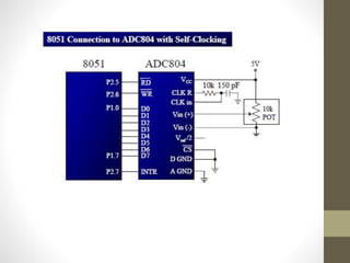
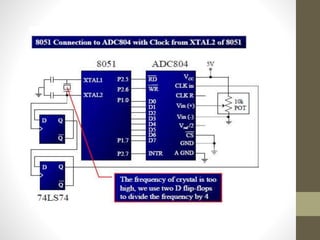
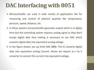
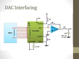
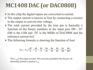
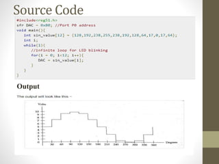
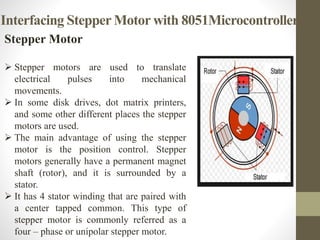
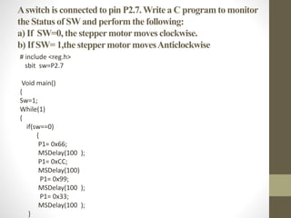
S. Y. B. Sc. (Computer Science)
SEM – III
Electronics Paper I
ADC and DAC interfacing with 8051
Presentation
By
Mrs. Neeta Gatkal
Head, Department of Electronics
Pratibha College of Computer and Computer Studies,Chinchwad
INTERFACING TO ADC AND SENSORS
 ADCs (analog-to-digital converters) are among the most
widely used devices for data acquisition
 A physical quantity, like temperature, pressure, humidity, and
velocity, etc., is converted to electrical (voltage, current)
signals using a device called a transducer, or sensor
 We need an analog-to-digital converter to translate the analog
signals to digital numbers, so microcontroller can read them
ADC804 IC is an analog-to-digital converter
• It works with +5 volts and has a resolution of 8 bits
• Conversion time is another major factor in judging an
ADC
 Conversion time is defined as the time it takes the
ADC to convert the analog input to a digital (binary)
number
 In ADC804 conversion time varies depending on
the clocking signals applied to CLK R and CLK IN pins,
but it cannot be faster than 110 ms
Testing ADC0804
Resolution:
The resolution of an ADC is how accurately it will sample
(convert) the analog signals into digital values (i.e. 0s and
1s). Higher is the resolution then greater will be the
accuracy.
Step size:
It is the minimum voltage change that measures by the
ADC. In other words you can say that the step size is the
voltage difference between one digital level (i.e. 0001) and
the next digital level (i.e. 0010 or 0000). For example, If a
4bit ADC has the step size 1 volt then if we will give the 1
volt as input the output will be 0001.
CS: Chip Select
It is an active low pin and is used to activate ADC0804
RD: Read Pin
It is an input pin and active at low. ADC stores the result in an
internal register after the conversion of analog data. This pin helps to
get the data out of the ADC0804. When CS=0, high to low pulse is
given to RD pin, then digital output comes on the pins D0-D7
WR: Write Pin
It is an input pin and is active low which is used to initiate the ADC
to start the conversion process.
When CS=0, WR makes a low to high transition, then ADC starts the
conversion process.
INTR: Interrupt
This is an output pin and is active low. When the conversion is over,
this pin goes low.
Vin+: Analog Input
Analog input to ADC.
Vin-: Analog Input.
Analog input connected to the ground.
 CLK IN and CLK R
CLK IN is an input pin connected to an external clock
source
To use the internal clock generator (also called self-
clocking), CLK IN and CLK R pins are connected to a
capacitor and a resistor, and the clock frequency is
determined by
 f = 1/1.1RC
 Typical values are R = 10K ohms and C = 150 pF
 We get f = 606 kHz and the conversion time is 110 us
Vref/2
It is used for the reference voltage
If this pin is open (not connected), the analog input voltage is in
the range of 0 to 5 volts (the same as the Vcc pin)
If the analog input range needs to be 0 to 4 volts, Vref/2 is
connected to 2 volts
D0-D7
The digital data output pins
These are tri-state buffered
The converted data is accessed only when CS = 0 and RD is forced
low
To calculate the output voltage, use the following
formula
Dout = Vin / Step Size
Dout = digital data output (in decimal),
Vin = analog voltage, and
step size (resolution) is the smallest change
Conversion Steps of ADC0804
1. Make CS = 0.
2. Send a low-to-high pulse to pin WR to start the
conversion.
3. Monitor the INTR pin. If INTR is low, the conversion is
finished but if the INTR is high, keep polling until it goes
low.
4. After the INTR has become low, we make CS = 0 and
send a high-to-low pulse to the RD pin to get the data out of
the ADC804.
DAC Interfacing with 8051
 Microcontroller are used in wide variety of applications like for
measuring and control of physical quantity like temperature,
pressure, speed, distance, etc.
 In these systems microcontroller generates output which is in digital
form but the controlling system requires analog signal as they don't
accept digital data thus making it necessary to use DAC which
converts digital data into equivalent analog voltage.
 In the figure shown, we use 8-bit DAC 0808. This IC converts digital
data into equivalent analog Current. Hence we require an I to V
converter to convert this current into equivalent voltage.
DAC Interfacing
MC1408 DAC (or DAC0808)
In this chip the digital inputs are converted to current.
The output current is known as Iout by connecting a resistor
to the output to convert into voltage.
The total current provided by the Iout pin is basically a
function of the binary numbers at the input pins D0 - D7
(D0 is the LSB and D7 is the MSB) of DAC0808 and the
reference current Iref.
The following formula is showing the function of Iout
The I ref is the input current. This must be provided into the pin 14.
Generally 2.0mA is used as I ref
GeneratingSine wave using DAC and8051
DAC input values = 5v*25.6 =128
Source Code
Output
Interfacing Stepper Motor with 8051Microcontroller
Stepper Motor
 Stepper motors are used to translate
electrical pulses into mechanical
movements.
 In some disk drives, dot matrix printers,
and some other different places the stepper
motors are used.
 The main advantage of using the stepper
motor is the position control. Stepper
motors generally have a permanent magnet
shaft (rotor), and it is surrounded by a
stator.
 It has 4 stator winding that are paired with
a center tapped common. This type of
stepper motor is commonly referred as a
four – phase or unipolar stepper motor.
Some parameters of stepper motors
Step Angle − The step angle is the angle in which the rotor
moves when one pulse is applied as an input of the stator.
This parameter is used to determine the positioning of a
stepper motor.
Steps per Revolution − This is the number of step angles
required for a complete revolution. So the formula is 360°
/Step Angle.
Steps per Second − This parameter is used to measure a
number of steps covered in each second.
RPM − The RPM is the Revolution Per Minute. It measures
the frequency of rotation. By this parameter, we can measure
the number of rotations in one minute.
Switching Sequence of motor
The Unipolar stepper motor works in three modes.
Wave Drive Mode − In this mode, one coil is energized at a time. So
all four coils are energized one after another. This mode produces
less torque than full step drive mode.
The following table is showing the sequence of input states in
different windings.
Full Drive Mode − In this mode, two coils are energized at
the same time. This mode produces more torque. Here the
power consumption is also high
The following table is showing the sequence of input states in different windings.
Half Drive Mode − In this mode, one and two coils are
energized alternately. At first, one coil is energized then two
coils are energized. This is basically a combination of wave
and full drive mode. It increases the angular rotation of the
motor.
The following table is showing the sequence of input states
in different windings.
Describe the 8051 connection to the stepper motor and write
a program to rotate it continuously.
MOV A, #66H ; LOAD THE STEP SEQUENCE
BACK :
MOV P1, A ; LOAD SEQUENCE TO PORT
RR A ; CHANGE SEQUENCE ROTATE CLOCKWISE
ACALL DELAY : WAIT FOR IT
SJMP BACK ; NOW KEEP GOING
DELAY :
MOV R2, #100
H1 :
MOV R3, #255
H2 :
DJNZ R3, H2
DJNZ R2, H1
RET
END
Aswitch is connected to pin P2.7.Write a C program to monitor
the Status of SWand perform the following:
a) If SW=0, the steppermotormoves clockwise.
b) If SW= 1,the steppermotormovesAnticlockwise
# include <reg.h>
sbit sw=P2.7
Void main()
{
Sw=1;
While(1)
{
if(sw==0)
{
P1= 0x66;
MSDelay(100 );
P1= 0xCC;
MSDelay(100)
P1= 0x99;
MSDelay(100 );
P1= 0x33;
MSDelay(100 );
}

Adc and dac

  • 1.
    S. Y. B.Sc. (Computer Science) SEM – III Electronics Paper I ADC and DAC interfacing with 8051 Presentation By Mrs. Neeta Gatkal Head, Department of Electronics Pratibha College of Computer and Computer Studies,Chinchwad
  • 2.
    INTERFACING TO ADCAND SENSORS  ADCs (analog-to-digital converters) are among the most widely used devices for data acquisition  A physical quantity, like temperature, pressure, humidity, and velocity, etc., is converted to electrical (voltage, current) signals using a device called a transducer, or sensor  We need an analog-to-digital converter to translate the analog signals to digital numbers, so microcontroller can read them
  • 3.
    ADC804 IC isan analog-to-digital converter • It works with +5 volts and has a resolution of 8 bits • Conversion time is another major factor in judging an ADC  Conversion time is defined as the time it takes the ADC to convert the analog input to a digital (binary) number  In ADC804 conversion time varies depending on the clocking signals applied to CLK R and CLK IN pins, but it cannot be faster than 110 ms
  • 4.
  • 5.
    Resolution: The resolution ofan ADC is how accurately it will sample (convert) the analog signals into digital values (i.e. 0s and 1s). Higher is the resolution then greater will be the accuracy. Step size: It is the minimum voltage change that measures by the ADC. In other words you can say that the step size is the voltage difference between one digital level (i.e. 0001) and the next digital level (i.e. 0010 or 0000). For example, If a 4bit ADC has the step size 1 volt then if we will give the 1 volt as input the output will be 0001. CS: Chip Select It is an active low pin and is used to activate ADC0804
  • 6.
    RD: Read Pin Itis an input pin and active at low. ADC stores the result in an internal register after the conversion of analog data. This pin helps to get the data out of the ADC0804. When CS=0, high to low pulse is given to RD pin, then digital output comes on the pins D0-D7 WR: Write Pin It is an input pin and is active low which is used to initiate the ADC to start the conversion process. When CS=0, WR makes a low to high transition, then ADC starts the conversion process. INTR: Interrupt This is an output pin and is active low. When the conversion is over, this pin goes low. Vin+: Analog Input Analog input to ADC. Vin-: Analog Input. Analog input connected to the ground.
  • 7.
     CLK INand CLK R CLK IN is an input pin connected to an external clock source To use the internal clock generator (also called self- clocking), CLK IN and CLK R pins are connected to a capacitor and a resistor, and the clock frequency is determined by  f = 1/1.1RC  Typical values are R = 10K ohms and C = 150 pF  We get f = 606 kHz and the conversion time is 110 us
  • 8.
    Vref/2 It is usedfor the reference voltage If this pin is open (not connected), the analog input voltage is in the range of 0 to 5 volts (the same as the Vcc pin) If the analog input range needs to be 0 to 4 volts, Vref/2 is connected to 2 volts
  • 9.
    D0-D7 The digital dataoutput pins These are tri-state buffered The converted data is accessed only when CS = 0 and RD is forced low To calculate the output voltage, use the following formula Dout = Vin / Step Size Dout = digital data output (in decimal), Vin = analog voltage, and step size (resolution) is the smallest change
  • 10.
    Conversion Steps ofADC0804 1. Make CS = 0. 2. Send a low-to-high pulse to pin WR to start the conversion. 3. Monitor the INTR pin. If INTR is low, the conversion is finished but if the INTR is high, keep polling until it goes low. 4. After the INTR has become low, we make CS = 0 and send a high-to-low pulse to the RD pin to get the data out of the ADC804.
  • 13.
    DAC Interfacing with8051  Microcontroller are used in wide variety of applications like for measuring and control of physical quantity like temperature, pressure, speed, distance, etc.  In these systems microcontroller generates output which is in digital form but the controlling system requires analog signal as they don't accept digital data thus making it necessary to use DAC which converts digital data into equivalent analog voltage.  In the figure shown, we use 8-bit DAC 0808. This IC converts digital data into equivalent analog Current. Hence we require an I to V converter to convert this current into equivalent voltage.
  • 14.
  • 15.
    MC1408 DAC (orDAC0808) In this chip the digital inputs are converted to current. The output current is known as Iout by connecting a resistor to the output to convert into voltage. The total current provided by the Iout pin is basically a function of the binary numbers at the input pins D0 - D7 (D0 is the LSB and D7 is the MSB) of DAC0808 and the reference current Iref. The following formula is showing the function of Iout The I ref is the input current. This must be provided into the pin 14. Generally 2.0mA is used as I ref
  • 16.
    GeneratingSine wave usingDAC and8051 DAC input values = 5v*25.6 =128
  • 17.
  • 18.
    Interfacing Stepper Motorwith 8051Microcontroller Stepper Motor  Stepper motors are used to translate electrical pulses into mechanical movements.  In some disk drives, dot matrix printers, and some other different places the stepper motors are used.  The main advantage of using the stepper motor is the position control. Stepper motors generally have a permanent magnet shaft (rotor), and it is surrounded by a stator.  It has 4 stator winding that are paired with a center tapped common. This type of stepper motor is commonly referred as a four – phase or unipolar stepper motor.
  • 19.
    Some parameters ofstepper motors Step Angle − The step angle is the angle in which the rotor moves when one pulse is applied as an input of the stator. This parameter is used to determine the positioning of a stepper motor. Steps per Revolution − This is the number of step angles required for a complete revolution. So the formula is 360° /Step Angle. Steps per Second − This parameter is used to measure a number of steps covered in each second. RPM − The RPM is the Revolution Per Minute. It measures the frequency of rotation. By this parameter, we can measure the number of rotations in one minute.
  • 20.
    Switching Sequence ofmotor The Unipolar stepper motor works in three modes. Wave Drive Mode − In this mode, one coil is energized at a time. So all four coils are energized one after another. This mode produces less torque than full step drive mode. The following table is showing the sequence of input states in different windings.
  • 21.
    Full Drive Mode− In this mode, two coils are energized at the same time. This mode produces more torque. Here the power consumption is also high The following table is showing the sequence of input states in different windings.
  • 22.
    Half Drive Mode− In this mode, one and two coils are energized alternately. At first, one coil is energized then two coils are energized. This is basically a combination of wave and full drive mode. It increases the angular rotation of the motor. The following table is showing the sequence of input states in different windings.
  • 23.
    Describe the 8051connection to the stepper motor and write a program to rotate it continuously. MOV A, #66H ; LOAD THE STEP SEQUENCE BACK : MOV P1, A ; LOAD SEQUENCE TO PORT RR A ; CHANGE SEQUENCE ROTATE CLOCKWISE ACALL DELAY : WAIT FOR IT SJMP BACK ; NOW KEEP GOING DELAY : MOV R2, #100 H1 : MOV R3, #255 H2 : DJNZ R3, H2 DJNZ R2, H1 RET END
  • 24.
    Aswitch is connectedto pin P2.7.Write a C program to monitor the Status of SWand perform the following: a) If SW=0, the steppermotormoves clockwise. b) If SW= 1,the steppermotormovesAnticlockwise # include <reg.h> sbit sw=P2.7 Void main() { Sw=1; While(1) { if(sw==0) { P1= 0x66; MSDelay(100 ); P1= 0xCC; MSDelay(100) P1= 0x99; MSDelay(100 ); P1= 0x33; MSDelay(100 ); }