Download to read offline
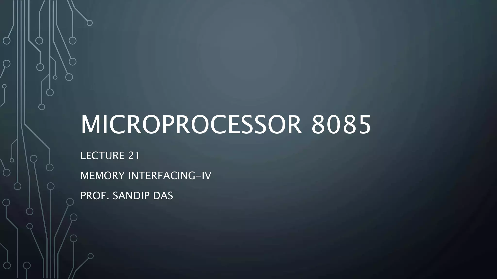
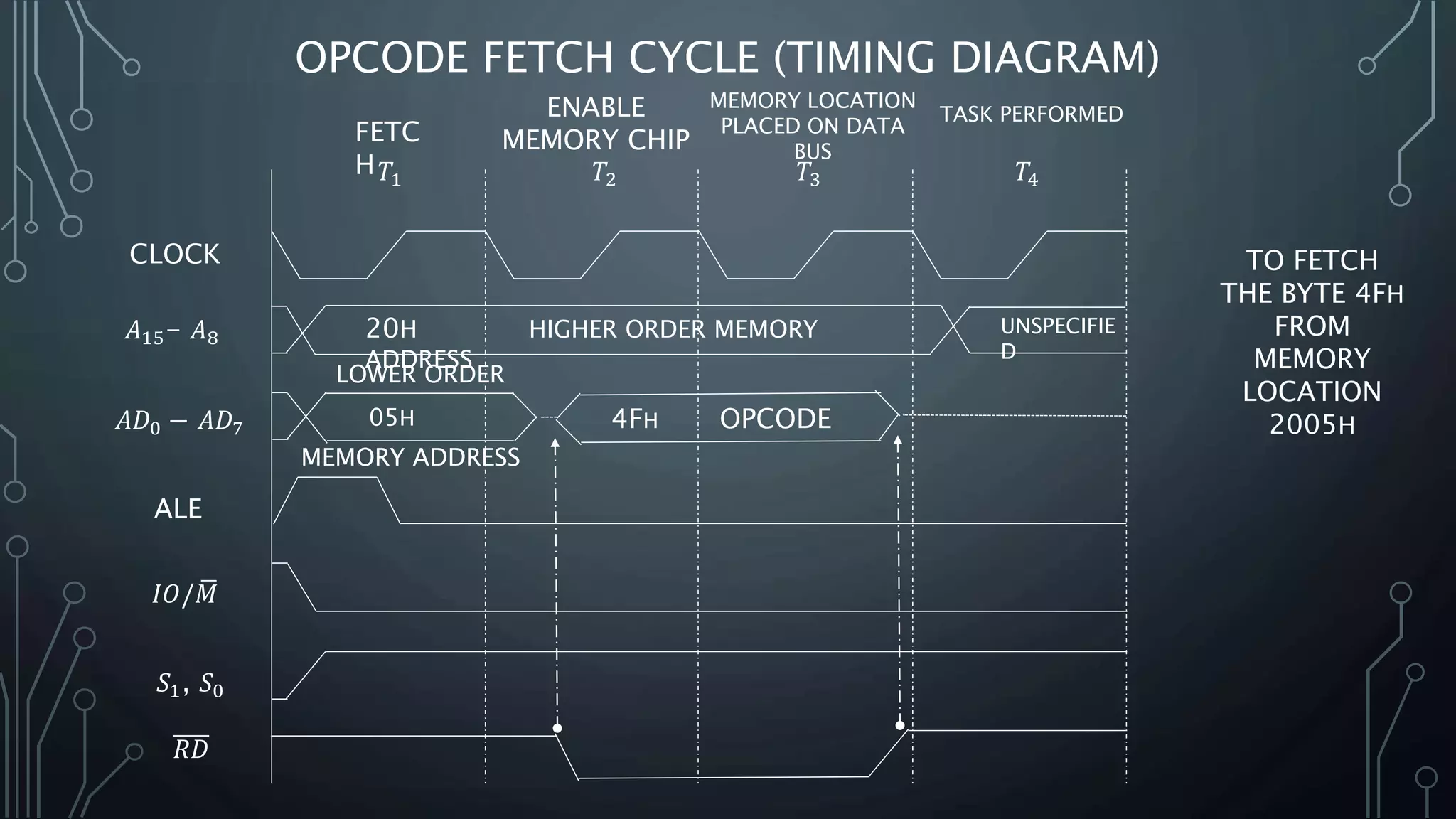
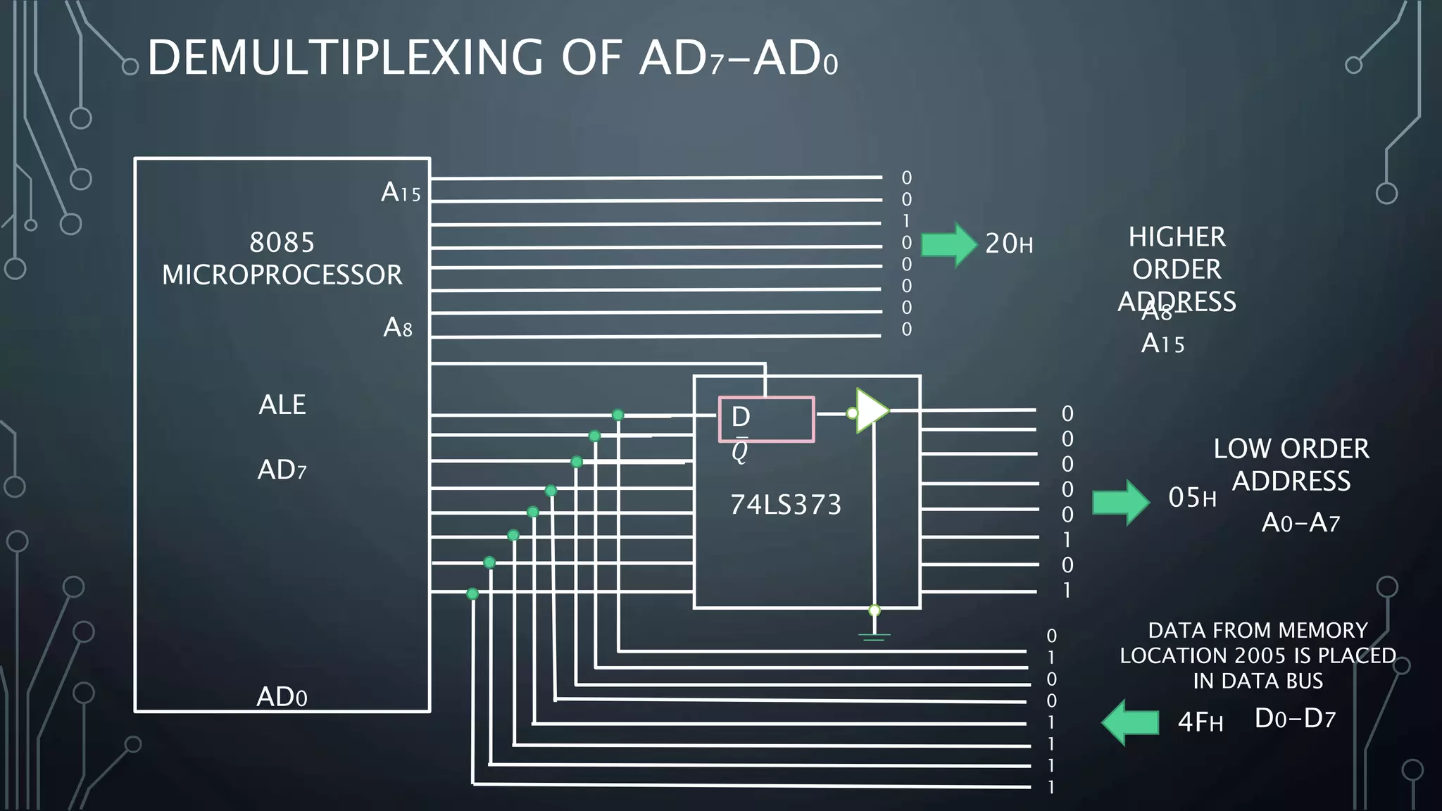
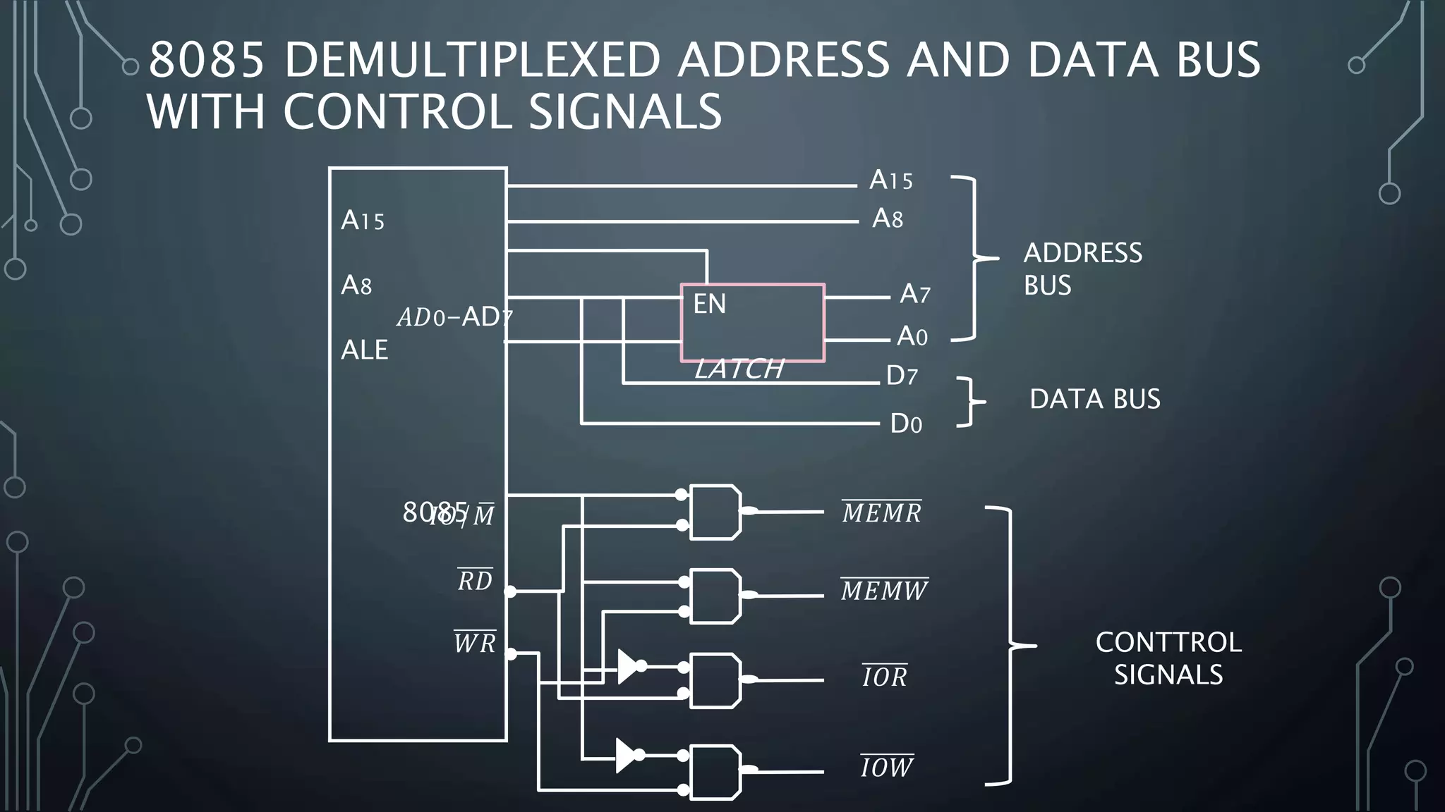

This document discusses the opcode fetch cycle of the 8085 microprocessor. It contains timing diagrams and explanations of how the microprocessor generates control signals to fetch opcodes from memory. It shows how the 8085 demultiplexes the address and data buses to access specific memory locations and place the fetched opcode on the data bus. Control signals like IO/M, RD, ALE are generated and used to latch the lower order address and retrieve the opcode byte from the addressed memory location during fetch.