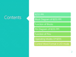
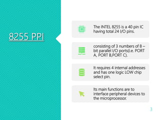
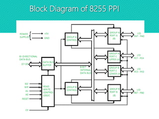
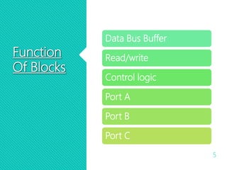
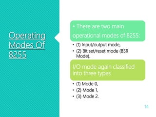
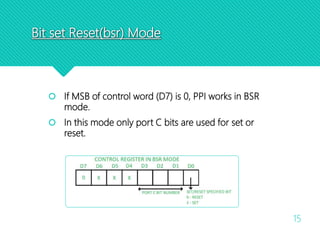
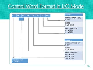
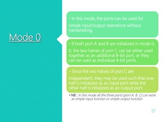
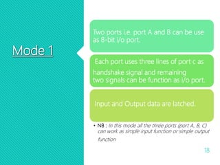
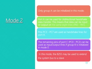
Programmable peripheral
interface 8255
Md. Marajul Islam
ID:16CSE038
Contents
2
8255 PPI
Block Diagram of 8255 PPI
Function of Blocks
Pin Diagram of 8255 PPI
Function of Pins
Operating Modes Of 8255
Control Word Format in I/O mode
8255 PPI
3
The INTEL 8255 is a 40 pin IC
having total 24 I/O pins.
consisting of 3 numbers of 8 –
bit parallel I/O ports(i.e. PORT
A, PORT B,PORT C).
It requires 4 internal addresses
and has one logic LOW chip
select pin.
Its main functions are to
interface peripheral devices to
the microprocessor.
Block Diagram of 8255 PPI
4
Function
Of Blocks
5
Data Bus Buffer
Read/write
Control logic
Port A
Port B
Port C
8255 – Block diagram Description
Data Bus Buffer
This three-state bi-directional 8-bit buffer is used to interface the 8255
to the system data bus. Data is transmitted or received by the buffer
upon execution of input or output instructions by the CPU. Control
words and status information are also transferred through the data bus
buffer.
Read/Write and Control Logic
The function of this block is to manage all of the internal and external
transfers of both Data and Control or Status words. It accepts inputs
from the CPU Address and Control busses and in turn, issues
commands to both of the Control Groups.
6
8255 – Block diagram Description
 (CS) Chip Select. A "low" on this input pin enables the
communication between the 8255 and the CPU.
 (RD) Read. A "low" on this input pin enables 8255 to send the data
or status information to the CPU on the data bus. In essence, it
allows the CPU to "read from" the 8255.
 (WR) Write. A "low" on this input pin enables the CPU to write data
or control words into the 8255.
 (RESET) Reset. A "high" on this input initializes the control register
to 9Bh and all ports (A, B, C) are set to the input mode.
7
8255 – Block diagram Description
 (A0 and A1) Port Select 0 and Port Select 1. These input signals, in
conjunction with the RD and WR inputs, control the selection of
one of the three ports or the control word register. They are
normally connected to the least significant bits of the address bus
(A0 and A1).
8
8255 – Block diagram Description
Group A and Group B Controls
 The functional configuration of each port is programmed by the
systems software. In essence, the CPU "outputs" a control word
to the 8255. The control word contains information such as
"model", "bit set", "bit reset", etc., that initializes the
functional configuration of the 8255. Each of the Control blocks
(Group A and Group B) accepts "commands" from the
Read/Write Control logic, receives "control words" from the
internal data bus and issues the proper commands to its
associated ports.
9
8255 – Block diagram Description
 Port A One 8-bit data output latch/buffer and one 8-bit data input
latch.
 Port B One 8-bit data input/output latch/buffer and one 8-bit data
input buffer.
 Port C One 8-bit data output latch/buffer and one 8-bit data input
buffer (no latch for input). This port can be divided into two 4-bit
ports under the mode control. Each 4-bit port contains a 4-bit
latch and it can be used for the control signal output and status
signal inputs in conjunction with ports A and B.
10
PIN
DIAGRAM
OF 8255
PPI
11
Function
Of Pin
12
D0-D7 (Data Bus)
PA0-PA7 (Port A)
PB0-PB7 (Port B)
PC0-PC7 ((Port C)
RD
WR
CS
RESET
A0-A1
Interfacing 8255 with 8085 processor
13
Operating
Modes Of
8255
14
• There are two main
operational modes of 8255:
• (1) Input/output mode,
• (2) Bit set/reset mode (BSR
Mode).
I/O mode again classified
into three types
• (1) Mode 0,
• (2) Mode 1,
• (3) Mode 2.
Bit set Reset(bsr) Mode
15
 If MSB of control word (D7) is 0, PPI works in BSR
mode.
 In this mode only port C bits are used for set or
reset.
Control Word Format in I/O Mode
16
Mode 0
17
• In this mode, the ports can be used for
simple input/output operations without
handshaking.
• If both port A and B are initialized in mode 0,
0, the two halves of port C can be either used
together as an additional 8-bit port, or they
can be used as individual 4-bit ports.
• Since the two halves of port C are
independent, they may be used such that one-
half is initialized as an input port while the
other half is initialized as an output port.
• NB : In this mode all the three ports (port A, B, C) can work
as simple input function or simple output function
Mode 1
18
Two ports i.e. port A and B can be use
as 8-bit i/o port.
Each port uses three lines of port c as
handshake signal and remaining
two signals can be function as i/o port.
Input and Output data are latched.
• NB : In this mode all the three ports (port A, B, C)
can work as simple input function or simple output
function
Mode 2
19
Only group A can be initialized in this mode.
Port A can be used for bidirectional handshake
data transfer. This means that data can be input
or output on the same eight lines (PA0 - PA7).
Pins PC3 - PC7 are used as handshake lines for
port A.
The remaining pins of port C (PC0 - PC2) can be
used as input/output lines if group B is initialized
in mode 0.
In this mode, the 8255 may be used to extend
the system bus to a slave
THE END
20

Programmable peripheral interface 8255

  • 1.
  • 2.
    Contents 2 8255 PPI Block Diagramof 8255 PPI Function of Blocks Pin Diagram of 8255 PPI Function of Pins Operating Modes Of 8255 Control Word Format in I/O mode
  • 3.
    8255 PPI 3 The INTEL8255 is a 40 pin IC having total 24 I/O pins. consisting of 3 numbers of 8 – bit parallel I/O ports(i.e. PORT A, PORT B,PORT C). It requires 4 internal addresses and has one logic LOW chip select pin. Its main functions are to interface peripheral devices to the microprocessor.
  • 4.
    Block Diagram of8255 PPI 4
  • 5.
    Function Of Blocks 5 Data BusBuffer Read/write Control logic Port A Port B Port C
  • 6.
    8255 – Blockdiagram Description Data Bus Buffer This three-state bi-directional 8-bit buffer is used to interface the 8255 to the system data bus. Data is transmitted or received by the buffer upon execution of input or output instructions by the CPU. Control words and status information are also transferred through the data bus buffer. Read/Write and Control Logic The function of this block is to manage all of the internal and external transfers of both Data and Control or Status words. It accepts inputs from the CPU Address and Control busses and in turn, issues commands to both of the Control Groups. 6
  • 7.
    8255 – Blockdiagram Description  (CS) Chip Select. A "low" on this input pin enables the communication between the 8255 and the CPU.  (RD) Read. A "low" on this input pin enables 8255 to send the data or status information to the CPU on the data bus. In essence, it allows the CPU to "read from" the 8255.  (WR) Write. A "low" on this input pin enables the CPU to write data or control words into the 8255.  (RESET) Reset. A "high" on this input initializes the control register to 9Bh and all ports (A, B, C) are set to the input mode. 7
  • 8.
    8255 – Blockdiagram Description  (A0 and A1) Port Select 0 and Port Select 1. These input signals, in conjunction with the RD and WR inputs, control the selection of one of the three ports or the control word register. They are normally connected to the least significant bits of the address bus (A0 and A1). 8
  • 9.
    8255 – Blockdiagram Description Group A and Group B Controls  The functional configuration of each port is programmed by the systems software. In essence, the CPU "outputs" a control word to the 8255. The control word contains information such as "model", "bit set", "bit reset", etc., that initializes the functional configuration of the 8255. Each of the Control blocks (Group A and Group B) accepts "commands" from the Read/Write Control logic, receives "control words" from the internal data bus and issues the proper commands to its associated ports. 9
  • 10.
    8255 – Blockdiagram Description  Port A One 8-bit data output latch/buffer and one 8-bit data input latch.  Port B One 8-bit data input/output latch/buffer and one 8-bit data input buffer.  Port C One 8-bit data output latch/buffer and one 8-bit data input buffer (no latch for input). This port can be divided into two 4-bit ports under the mode control. Each 4-bit port contains a 4-bit latch and it can be used for the control signal output and status signal inputs in conjunction with ports A and B. 10
  • 11.
  • 12.
    Function Of Pin 12 D0-D7 (DataBus) PA0-PA7 (Port A) PB0-PB7 (Port B) PC0-PC7 ((Port C) RD WR CS RESET A0-A1
  • 13.
    Interfacing 8255 with8085 processor 13
  • 14.
    Operating Modes Of 8255 14 • Thereare two main operational modes of 8255: • (1) Input/output mode, • (2) Bit set/reset mode (BSR Mode). I/O mode again classified into three types • (1) Mode 0, • (2) Mode 1, • (3) Mode 2.
  • 15.
    Bit set Reset(bsr)Mode 15  If MSB of control word (D7) is 0, PPI works in BSR mode.  In this mode only port C bits are used for set or reset.
  • 16.
    Control Word Formatin I/O Mode 16
  • 17.
    Mode 0 17 • Inthis mode, the ports can be used for simple input/output operations without handshaking. • If both port A and B are initialized in mode 0, 0, the two halves of port C can be either used together as an additional 8-bit port, or they can be used as individual 4-bit ports. • Since the two halves of port C are independent, they may be used such that one- half is initialized as an input port while the other half is initialized as an output port. • NB : In this mode all the three ports (port A, B, C) can work as simple input function or simple output function
  • 18.
    Mode 1 18 Two portsi.e. port A and B can be use as 8-bit i/o port. Each port uses three lines of port c as handshake signal and remaining two signals can be function as i/o port. Input and Output data are latched. • NB : In this mode all the three ports (port A, B, C) can work as simple input function or simple output function
  • 19.
    Mode 2 19 Only groupA can be initialized in this mode. Port A can be used for bidirectional handshake data transfer. This means that data can be input or output on the same eight lines (PA0 - PA7). Pins PC3 - PC7 are used as handshake lines for port A. The remaining pins of port C (PC0 - PC2) can be used as input/output lines if group B is initialized in mode 0. In this mode, the 8255 may be used to extend the system bus to a slave
  • 20.