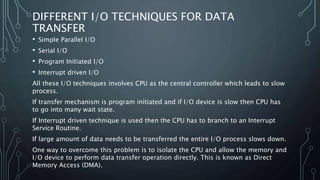
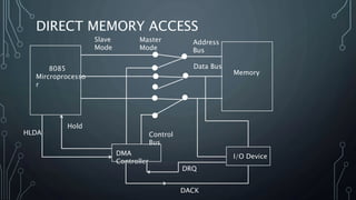
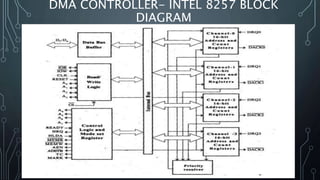
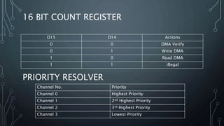
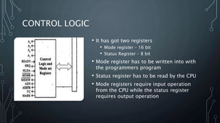
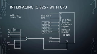
MICROPROCESSOR 8085
LECTURE 27
DIRECT MEMORY ACCESS (DMA)
DMA CONTROLLER (IC 8257)
PROF. SANDIP DAS
DIFFERENT I/O TECHNIQUES FOR DATA
TRANSFER
• Simple Parallel I/O
• Serial I/O
• Program Initiated I/O
• Interrupt driven I/O
All these I/O techniques involves CPU as the central controller which leads to slow
process.
If transfer mechanism is program initiated and if I/O device is slow then CPU has
to go into many wait state.
If Interrupt driven technique is used then the CPU has to branch to an Interrupt
Service Routine.
If large amount of data needs to be transferred the entire I/O process slows down.
One way to overcome this problem is to isolate the CPU and allow the memory and
I/O device to perform data transfer operation directly. This is known as Direct
Memory Access (DMA).
DIRECT MEMORY ACCESS
8085
Mircroprocesso
r
DMA
Controller
I/O Device
Memory
Address
Bus
Data Bus
Control
Bus
Hold
HLDA
DRQ
DACK
Slave
Mode
Master
Mode
DMA CONTROLLER- IC 8257
DMA CONTROLLER- INTEL 8257 BLOCK
DIAGRAM
CHANNEL
16 bit Address Register
• This registers are initially loaded by CPU when it is
Slave mode
• The address register contains 16 bit starting
address from which direct memory access starts.
• After every byte transfer this register is incremented
by 1.
• Count register is also 16 bit
16 bit Count Register
• Contains 14 bit count number and a 2 bit code.
This 2 bit code indicates the direction of DMA
transfer.
• The number of bytes that could be transferred is
214 = 16 𝐾𝐵 in one DMA operation.
D1
5
D14 D1
3
D0
Count
register
16 BIT COUNT REGISTER
D15 D14 Actions
0 0 DMA Verify
0 1 Write DMA
1 0 Read DMA
1 1 illegal
PRIORITY RESOLVER
Channel No. Priority
Channel 0 Highest Priority
Channel 1 2nd Highest Priority
Channel 2 3rd Highest Priority
Channel 3 Lowest Priority
CONTROL LOGIC
• It has got two registers
• Mode register – 16 bit
• Status Register – 8 bit
• Mode register has to be written into with
the programmers program
• Status register has to be read by the CPU
• Mode registers require input operation
from the CPU while the status register
requires output operation
MODE SET REGISTER
• Extended write is one in which 𝑀𝐸𝑀𝑊 and 𝐼𝑂𝑊 are made available to the
memory and the peripheral ahead of time by one clock period.
• When bit 6 is enabled it automatically disables the channel performing the
DMA transfer whenever the terminal count register of that channel reaches
zero.
• Bit 7 enables an autoload operation. This function is available only for
channel 2.
• If the channel 2 has to be disabled because the terminal count reached
zero, if the autoload has been set, i.e., Bit 7 is set, then the count will be
once again loaded into the count register.
• The DMA transfer will be permitted for the same number of times once
STATUS REGISTER
0 0 0
CH
0
CH
1
CH
2
CH
3
TC Status for different
channels
Update
flag
D0D7
• Only the lower four bits are useful.
• The status registers indicate
whether the channel are still in
count mode or has reached a
terminal count mode.
• D0, D1, D2, D3 will remain zero as
long as terminal count mode of
respective channel has not been
reached.
• In other words, if count register of a
channel has a non zero value then
respective bit of status register will
have zero value. If count register
has a zero value the respective bit
of status register will be set to 1.
• If auto load mode is used then
ADDRESS REGISTER (A3-A0)
A3 A2 A1 A0 Operations
0 0 0 0 CH-0 DMA ADDR. REGISTER
0 0 0 1 CH-0 COUNT REGISTER
0 0 1 0 CH-1 DMA ADDR. REGISTER
0 0 1 1 CH-1 COUNT REGISTER
0 1 0 0 CH-2 DMA ADDR. REGISTER
0 1 0 1 CH-2 COUNT REGISTER
0 1 1 0 CH-3 DMA ADDR. REGISTER
0 1 1 1 CH-3 COUNT REGISTER
1 0 0 0 MODE SET REGISTER (WITH
𝑊𝑅 CONTROL
1 0 0 0 MODE SET REGISTER (WITH
𝑅𝐷 CONTROL
INTERFACING IC 8257 WITH CPU
IC 8257
D
7
D
0
Data bus of
CPU
A7
A6
A5
A4
𝐼𝑂𝑅
𝐼𝑂𝑊 𝐶𝑆
5V
Addresses
70 H – 7F H
A3
A2
A1
A0
0
0
0
0
CH 0 Addr
Register0
0
0
1
CH 0 Count
Register
1
0
0
0
MODE set
Register
8257- MASTER MODE OPERATION
MEMORY
PERIPHERAL
𝐼𝑂𝑅
𝐼𝑂𝑊
8257
A7
A0
D
7D
0
A15
A0
𝑀𝐸𝑀𝑅
𝑀𝐸𝑀𝑊
DATA BUS
TC
ADSTB
AEN
HLD
A
HRQ
𝐷𝐴𝐶𝐾
DRQ

24. direct memory access

  • 1.
    MICROPROCESSOR 8085 LECTURE 27 DIRECTMEMORY ACCESS (DMA) DMA CONTROLLER (IC 8257) PROF. SANDIP DAS
  • 2.
    DIFFERENT I/O TECHNIQUESFOR DATA TRANSFER • Simple Parallel I/O • Serial I/O • Program Initiated I/O • Interrupt driven I/O All these I/O techniques involves CPU as the central controller which leads to slow process. If transfer mechanism is program initiated and if I/O device is slow then CPU has to go into many wait state. If Interrupt driven technique is used then the CPU has to branch to an Interrupt Service Routine. If large amount of data needs to be transferred the entire I/O process slows down. One way to overcome this problem is to isolate the CPU and allow the memory and I/O device to perform data transfer operation directly. This is known as Direct Memory Access (DMA).
  • 3.
    DIRECT MEMORY ACCESS 8085 Mircroprocesso r DMA Controller I/ODevice Memory Address Bus Data Bus Control Bus Hold HLDA DRQ DACK Slave Mode Master Mode
  • 4.
  • 5.
    DMA CONTROLLER- INTEL8257 BLOCK DIAGRAM
  • 6.
    CHANNEL 16 bit AddressRegister • This registers are initially loaded by CPU when it is Slave mode • The address register contains 16 bit starting address from which direct memory access starts. • After every byte transfer this register is incremented by 1. • Count register is also 16 bit 16 bit Count Register • Contains 14 bit count number and a 2 bit code. This 2 bit code indicates the direction of DMA transfer. • The number of bytes that could be transferred is 214 = 16 𝐾𝐵 in one DMA operation. D1 5 D14 D1 3 D0 Count register
  • 7.
    16 BIT COUNTREGISTER D15 D14 Actions 0 0 DMA Verify 0 1 Write DMA 1 0 Read DMA 1 1 illegal PRIORITY RESOLVER Channel No. Priority Channel 0 Highest Priority Channel 1 2nd Highest Priority Channel 2 3rd Highest Priority Channel 3 Lowest Priority
  • 8.
    CONTROL LOGIC • Ithas got two registers • Mode register – 16 bit • Status Register – 8 bit • Mode register has to be written into with the programmers program • Status register has to be read by the CPU • Mode registers require input operation from the CPU while the status register requires output operation
  • 9.
    MODE SET REGISTER •Extended write is one in which 𝑀𝐸𝑀𝑊 and 𝐼𝑂𝑊 are made available to the memory and the peripheral ahead of time by one clock period. • When bit 6 is enabled it automatically disables the channel performing the DMA transfer whenever the terminal count register of that channel reaches zero. • Bit 7 enables an autoload operation. This function is available only for channel 2. • If the channel 2 has to be disabled because the terminal count reached zero, if the autoload has been set, i.e., Bit 7 is set, then the count will be once again loaded into the count register. • The DMA transfer will be permitted for the same number of times once
  • 10.
    STATUS REGISTER 0 00 CH 0 CH 1 CH 2 CH 3 TC Status for different channels Update flag D0D7 • Only the lower four bits are useful. • The status registers indicate whether the channel are still in count mode or has reached a terminal count mode. • D0, D1, D2, D3 will remain zero as long as terminal count mode of respective channel has not been reached. • In other words, if count register of a channel has a non zero value then respective bit of status register will have zero value. If count register has a zero value the respective bit of status register will be set to 1. • If auto load mode is used then
  • 11.
    ADDRESS REGISTER (A3-A0) A3A2 A1 A0 Operations 0 0 0 0 CH-0 DMA ADDR. REGISTER 0 0 0 1 CH-0 COUNT REGISTER 0 0 1 0 CH-1 DMA ADDR. REGISTER 0 0 1 1 CH-1 COUNT REGISTER 0 1 0 0 CH-2 DMA ADDR. REGISTER 0 1 0 1 CH-2 COUNT REGISTER 0 1 1 0 CH-3 DMA ADDR. REGISTER 0 1 1 1 CH-3 COUNT REGISTER 1 0 0 0 MODE SET REGISTER (WITH 𝑊𝑅 CONTROL 1 0 0 0 MODE SET REGISTER (WITH 𝑅𝐷 CONTROL
  • 12.
    INTERFACING IC 8257WITH CPU IC 8257 D 7 D 0 Data bus of CPU A7 A6 A5 A4 𝐼𝑂𝑅 𝐼𝑂𝑊 𝐶𝑆 5V Addresses 70 H – 7F H A3 A2 A1 A0 0 0 0 0 CH 0 Addr Register0 0 0 1 CH 0 Count Register 1 0 0 0 MODE set Register
  • 13.
    8257- MASTER MODEOPERATION MEMORY PERIPHERAL 𝐼𝑂𝑅 𝐼𝑂𝑊 8257 A7 A0 D 7D 0 A15 A0 𝑀𝐸𝑀𝑅 𝑀𝐸𝑀𝑊 DATA BUS TC ADSTB AEN HLD A HRQ 𝐷𝐴𝐶𝐾 DRQ