
Recommended
More Related Content
What's hot
What's hot (20)
Similar to 8255 class
Similar to 8255 class (20)
Recently uploaded
Recently uploaded (20)
8255 class
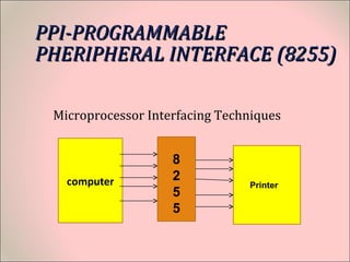
- 1. PPI-PROGRAMMABLEPPI-PROGRAMMABLE PHERIPHERAL INTERFACE (8255)PHERIPHERAL INTERFACE (8255) Microprocessor Interfacing Techniques computer Printer 8 2 5 5
- 2. Intel 8255A Programmable peripheral device It is a general purpose programmable i/o device which is designed for use with all intel and most other microprocessors for parallel data transfer (parallel i/o device)
- 3. Features 24 I/O ports (3 – 8 bit I/O ports PA, PB, PC) PC – PCU(4 bit) and PCL(4 bit) PA and PCU are Group A (GA) PB and PCL are Group B (GB) Can be programmed in two modes. 1. Bit set/reset mode BSR. 2. I/O mode BSR is used to set/reset bits in PC I/O mode – 1. mode 0 simple I/O 2. mode 1 I/O with handshake 3. mode 2 bidirectional I/O data transfer
- 4. Features I/O pins and their modes of operation can be programmed by writing each bits into the CONTROL WORD Reg PA can be set for Modes 0, 1, 2. PB for 0,1 PC for mode 0 and for BSR. Modes 1 and 2 are interrupt driven. Address/data bus must be externally demux'd.
- 6. D0 - D7 These are the data input/output lines for the device. All information read from and written to the 8255 occurs via these 8 data lines. CS (Chip Select Input). If this line is a logical 0, the microprocessor can read and write to the 8255. RD (Read Input) Whenever this input line is a low the CPU can read data in the ports or the status word, through the data buffer. WR (Write Input) Whenever this input line is low, the CPU can write data in the ports or in the control register through the data buffer.
- 7. A0 - A1 (Address Inputs) The logical combination of these two input lines determines which internal register of the 8255 data is written to or read from. RESET The 8255 is placed into its reset state if this input line is a logical 1. All peripheral ports are set to the input mode. PA0 - PA7, PB0 - PB7, PC0 - PC7 These signal lines are used as 8-bit I/O ports. They can be connected to peripheral devices. The 8255 has three 8 bit I/O ports and each one can be connected to the physical lines of an external device. These lines are labeled PA0-PA7, PB0-PB7, and PC0- PC7.
- 8. Port Selection A1 A0 Select 0 0 PA 0 1 PB 1 0 PC 1 1 Control reg.
- 9. Block diagram of the 8255
- 10. Data Bus buffer It is a 8-bit bidirectional Data bus. Used to interface between 8255 data bus with system bus. The internal data bus and Outer pins D0-D7 pins are connected in internally. The direction of data buffer is decided by Read/Control Logic.
- 11. Read/Write Control Logic This is getting the input signals from control bus and Address bus Control signal are RD and WR. Address signals are A0,A1,and CS. 8255 operation is enabled or disabled by CS.
- 12. Group A and Group B control Group A and B get the Control Signal from CPU and send the command to the individual control blocks. Group A send the control signal to port A and Port C (Upper) PC7-PC4. Group B send the control signal to port B and Port C (Lower) PC3-PC0. PORT A: This is a 8-bit buffered I/O latch. It can be programmed by mode 0 , mode 1, mode 2 .
- 13. PORT B: This is a 8-bit buffer I/O latch. It can be programmed by mode 0 and mode 1. PORT C: This is a 8-bit Unlatched buffer Input and an Output latch. It is splitted into two parts. It can be programmed by bit set/reset operation.
- 14. Operating modes Bit Set-Reset (BSR)mode I/O modes 1.Mode 0 2.Mode 1 3.Mode 2
- 15. Bit Set-Reset (BSR)mode The individual bits of Port C can be set or reset by sending out a single OUT instruction to control register
- 16. Bit set/reset control word format
- 17. PC0-PC7 is set or reset as per the status of D0. A BSR word is written for each bit Example: PC3 is Set then control register will be 0XXX0111. PC4 is Reset then control register will be 0XXX01000. X is a don’t care.
- 19. I/O MODES MODE 0 Each of the 3 ports can be programmed to be either an input/output. No handshaking is required. Features - outputs are latched - Inputs are buffered, not latched -ports do not have handshake or interrupt capability
- 20. I/O MODES MODE 0
- 21. MODE 1 Ports A and B are programmed to have 8 lines of input or output 3 pins of PC in each group are used for handshaking and interrupt control signals, and one is used for simple I/O functions I/O are latched. Interrupt logic is supported.
- 22. MODE 1
- 23. I/p ctrl signalsI/p ctrl signals Processor 8 2 5 5 Peripheral Device (Keyboard) STB IBF RD INTR
- 24. Mode 1 Input control SignalsMode 1 Input control Signals
- 27. O/p Ctrl Signals Processor 8 2 5 5 Peripheral Device (Printer) OBF WR INTR data data ACK
- 30. MODE 2 It is a strobed bi-directional bus configuration. This feature is available only in GroupA with port A as 8-bit bidirectional data bus ; and PC3-PC7 are used for handshaking purpose
- 31. Mode 2 –Bi-directional Operation WR RD
- 32. Mode Definition Summary MODE 0 MODE 1 MODE 2 IN OUT IN OUT Group A only PA (0-7) YES YES YES YES PB (0-7) YES YES YES YES In mode 0 or mode 1 only PC (0-7) YES YES PC0 - INTRB PC1 - IBFB PC2 - STBB PC3 - INTRA PC4 - STBA PC5 - IBFA PC6 - I/O PC7 - I/O PC0 - INTRB PC1 - OBFB PC2 - ACKB PC3 - INTRA PC4 - I/O PC5 - I/O PC6 - ACKA PC7 - OBFA PC0 - I/O PC1 - I/O PC2 - I/O PC3 - INTRA PC4 - STBA PC5 - IBFA PC6 - ACKA PC7 - OBFA