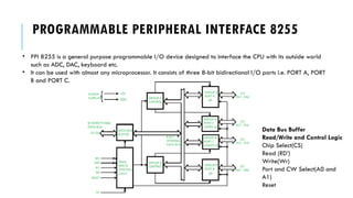
PROGRAMMABLE PERIPHERAL INTERFACE8255
• PPI 8255 is a general purpose programmable I/O device designed to interface the CPU with its outside world
such as ADC, DAC, keyboard etc.
• It can be used with almost any microprocessor. It consists of three 8-bit bidirectional I/O ports i.e. PORT A, PORT
B and PORT C.
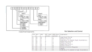
Data Bus Buffer
Read/Write and Control Logic
Chip Select(CS)
Read (RD’)
Write(Wr)
Port and CW Select(A0 and
A1)
Reset
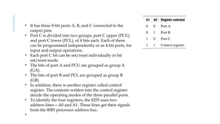
3.
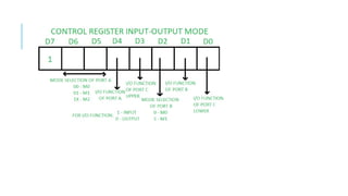
• It hasthree 8-bit ports A, B, and C connected to the
output pins.
• Port C is divided into two groups, port C upper (PCU)
and port C lower (PCL), of 4 bits each. Each of them
can be programmed independently or as 4-bit ports, for
input and output operations.
• Each port C bit can be set/reset individually in bit
set/reset mode.
• The bits of port A and PCU are grouped as group A
(GA).
• The bits of port B and PCL are grouped as group B
(GB).
• In addition, there is another register called control
register. The contents written into the control register
decide the operating modes of the three parallel ports.
• To identify the four registers, the 8255 uses two
address lines—A0 and A1. These lines get their signals
from the 8085 processor address bus.
•
4.
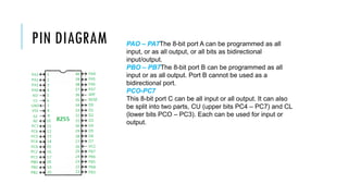
PIN DIAGRAM PAO– PA7The 8-bit port A can be programmed as all
input, or as all output, or all bits as bidirectional
input/output.
PBO – PB7The 8-bit port B can be programmed as all
input or as all output. Port B cannot be used as a
bidirectional port.
PCO-PC7
This 8-bit port C can be all input or all output. It can also
be split into two parts, CU (upper bits PC4 – PC7) and CL
(lower bits PCO – PC3). Each can be used for input or
output.
5.
• D0-D7 arethe lines required for interfacing the 8255
with the processor. These data lines are connected to
the data bus of the processor.
• The control signals for reading from and writing into
these registers are the active low RD and WR signals.
These signals are obtained from the processor’s control
signals.
• The chip is selected by activating the active low chip
select (CS) signal. This signal is obtained from the
decoder, which decodes the 8085 address lines and
identifies the 8255 address range.
• A common reset signal such as the RESET OUT of the
8085 processor can be applied to reset the 8255.
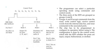
• The programmercan select a particular
operating mode using commands and
control words.
• The three ports of the 8255 are grouped as
groups A and B.
• Groups A and B accept commands from the
read/ write control logic, receive control
words from the internal data bus, and issue
commands to the associated ports.
• The chip has to be programmed to
configure its operation, before using it. The
configuration is done by the control word,
which tells the 8255 whether the ports are
input, output, bidirectional, or strobed.
9.
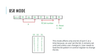
BSR MODE
This modeaffects only one bit of port C at a
time because, as user set the bit, it remains set
until and unless user changes it. User needs to
load the bit pattern in control register to change
the bit.