Downloaded 376 times
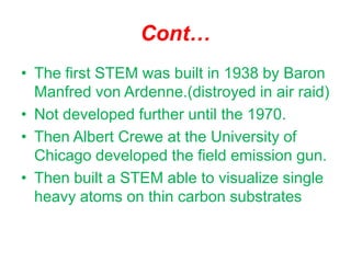

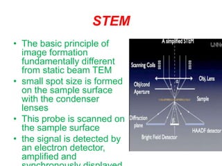
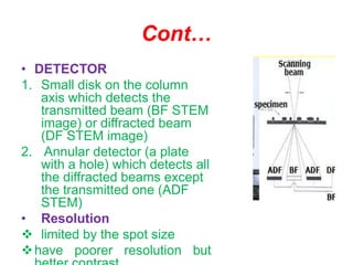
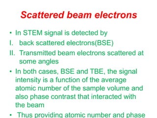
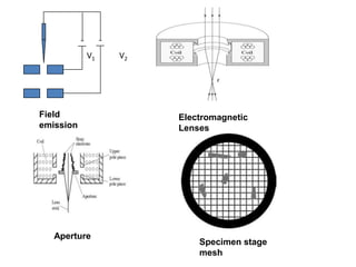
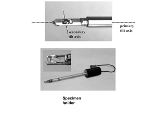
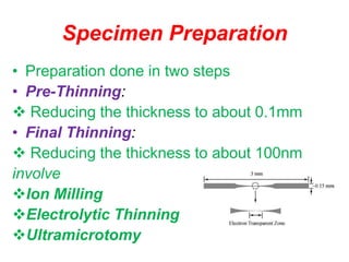
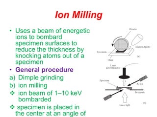

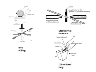
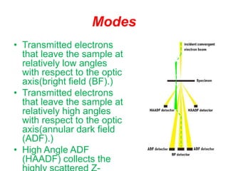
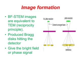
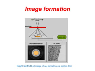
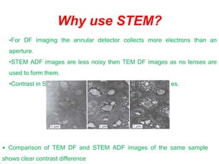


This document provides an overview of scanning transmission electron microscopy (STEM). It discusses the history and components of STEM, including the field emission gun, electromagnetic lenses, apertures, specimen stage, vacuum system, and detectors. Specimen preparation techniques like ion milling and electrolytic thinning are described. STEM operates by rastering a focused electron probe across the sample, while different detectors collect transmitted and scattered electrons to form images. Bright field (BF) and annular dark field (ADF) modes are covered, with ADF providing greater atomic number contrast. Advantages of STEM over conventional TEM are also highlighted.