Downloaded 1,538 times

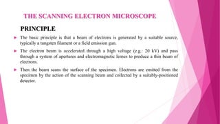

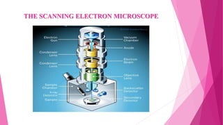
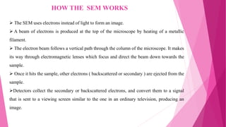


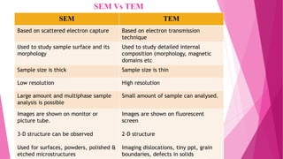


The document presents an overview of scanning electron microscopy (SEM), detailing its principle, construction, advantages, disadvantages, and applications. It explains how SEMs utilize electron beams to capture detailed images of specimen surfaces and provides information on components like electron guns, detectors, and the need for a vacuum. SEMs find applications across various fields, including materials science and biology, while being praised for their imaging capabilities and critiqued for their size and cost.