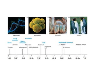
Electron microscopy provides high resolution imaging of nanoscale structures using electron beams. There are two main types: transmission electron microscopy (TEM) and scanning electron microscopy (SEM). TEM uses transmitted electrons to image ultra thin samples, allowing visualization of structures less than an angstrom in size. SEM scans a focused electron beam across a sample to generate topographical and compositional information from electron interactions within microns of the surface. Both techniques require specialized sample preparation and equipment to produce high quality images for research applications across biology, materials science, and other fields.
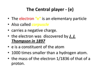

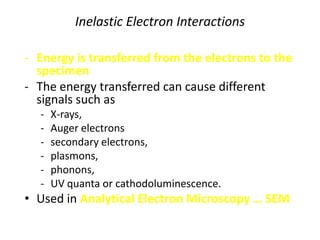
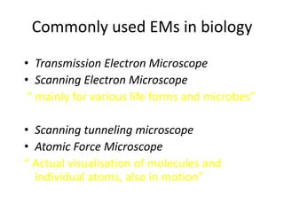
![• By taking multiple images of a
single TEM sample at differing
3D Imaging angles,
Three dimensional imaging -A TEM • typically in 1° increments,
image of a parapoxavirus
• a set of images known as a "tilt
series" can be collected.
• This methodology was proposed
in the 1970s by Walter Hoppe.
• Under absorption contrast
conditions, this set of images
can be used to construct a
three-dimensional
representation of the sample.[36]](https://image.slidesharecdn.com/electronmicroscopy-130121010455-phpapp01/85/Electron-microscopy-28-320.jpg)
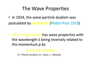
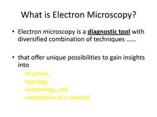
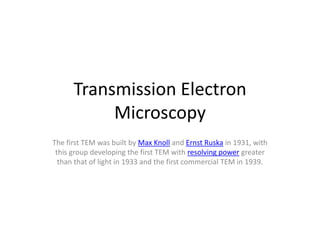
![3D data measurement
• 3D data can be measured in the SEM with
different methods such as:
- photogrammetry (2 or 3 images from tilted
specimen)
- photometric stereo (use of 4 images from BSE
detector)
- inverse reconstruction using electron-material
interactive models[31][32]
• Possible applications are roughness measurement, measurement of fractal
dimension, corrosion measurement and height step measurement.](https://image.slidesharecdn.com/electronmicroscopy-130121010455-phpapp01/85/Electron-microscopy-43-320.jpg)
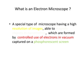
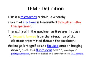
![Biological sample preparation
• Chemical fixation with Gluteraldehyde, optionally with OsO4 – for soft tissues
• No fixation needed for dry specimen like bones, feathers etc
• Dehydration by replacement of water in the cells with organic solvents such as
ethanol or acetone, and replacement of these solvents in turn with a
transitional fluid such as liquid carbon dioxide by critical point drying.
• The carbon dioxide is removed while in a supercritical state, so that no gas-
liquid interface is formed within the sample during drying.
• The dry specimen is mounted on a specimen stub using epoxy resin
• ultrathin coating done by low-vacuum sputter coating or by high-vacuum
evaporation.
• Conductive materials in current use for specimen coating include gold,
gold/palladium alloy, platinum, osmium,[12] iridium, tungsten, chromium, and
graphite.](https://image.slidesharecdn.com/electronmicroscopy-130121010455-phpapp01/85/Electron-microscopy-44-320.jpg)