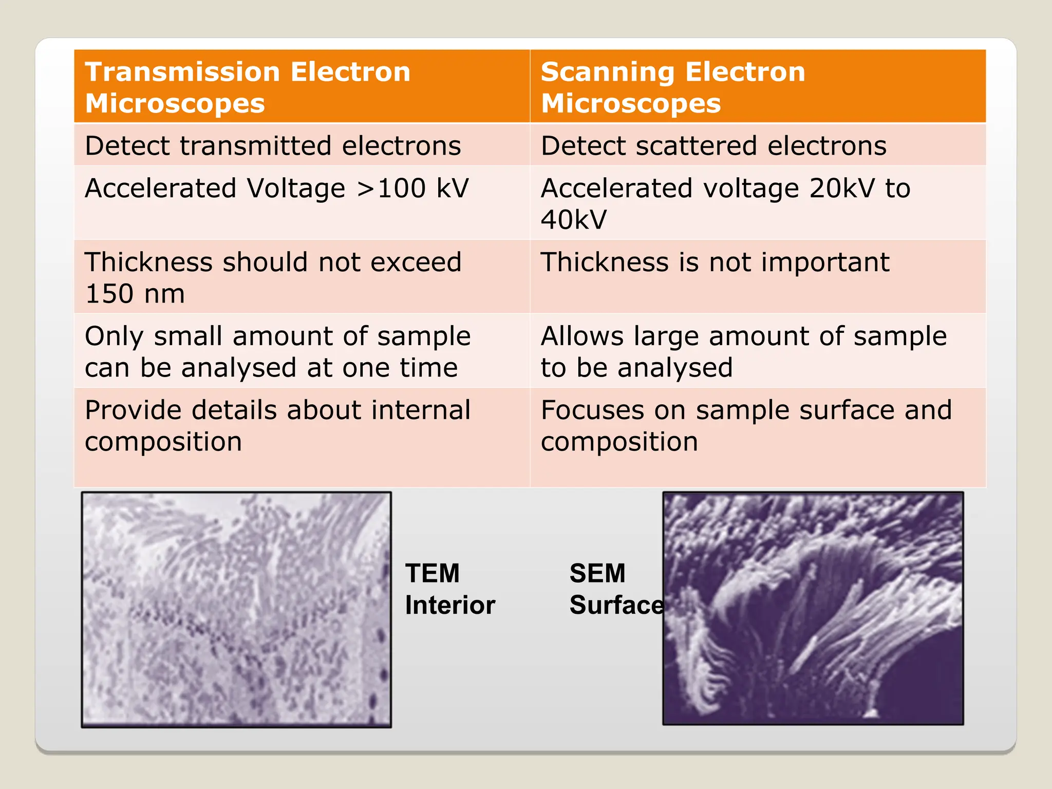
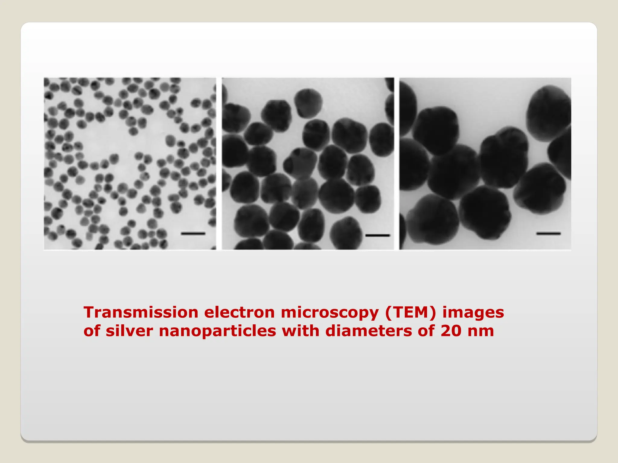
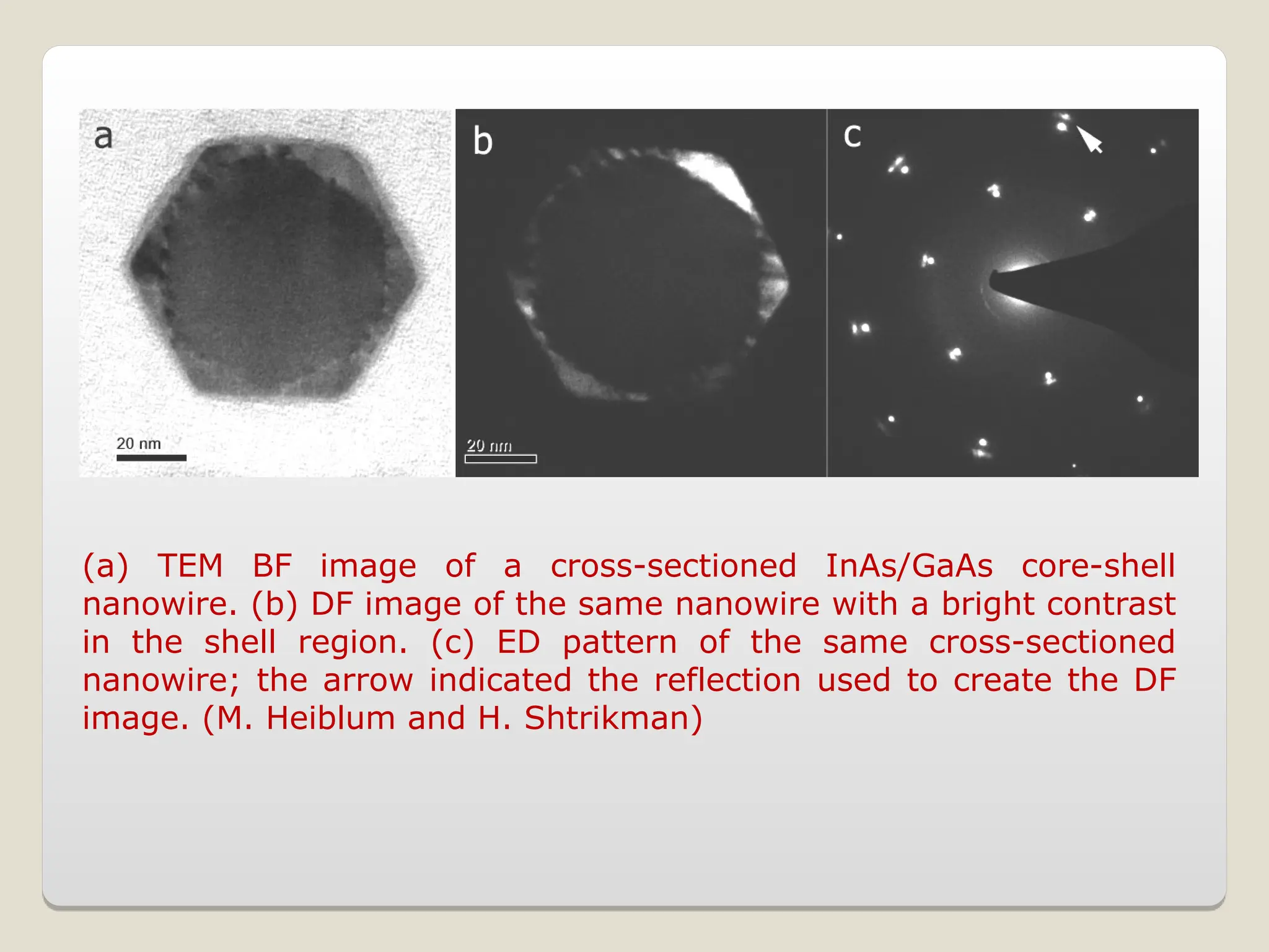
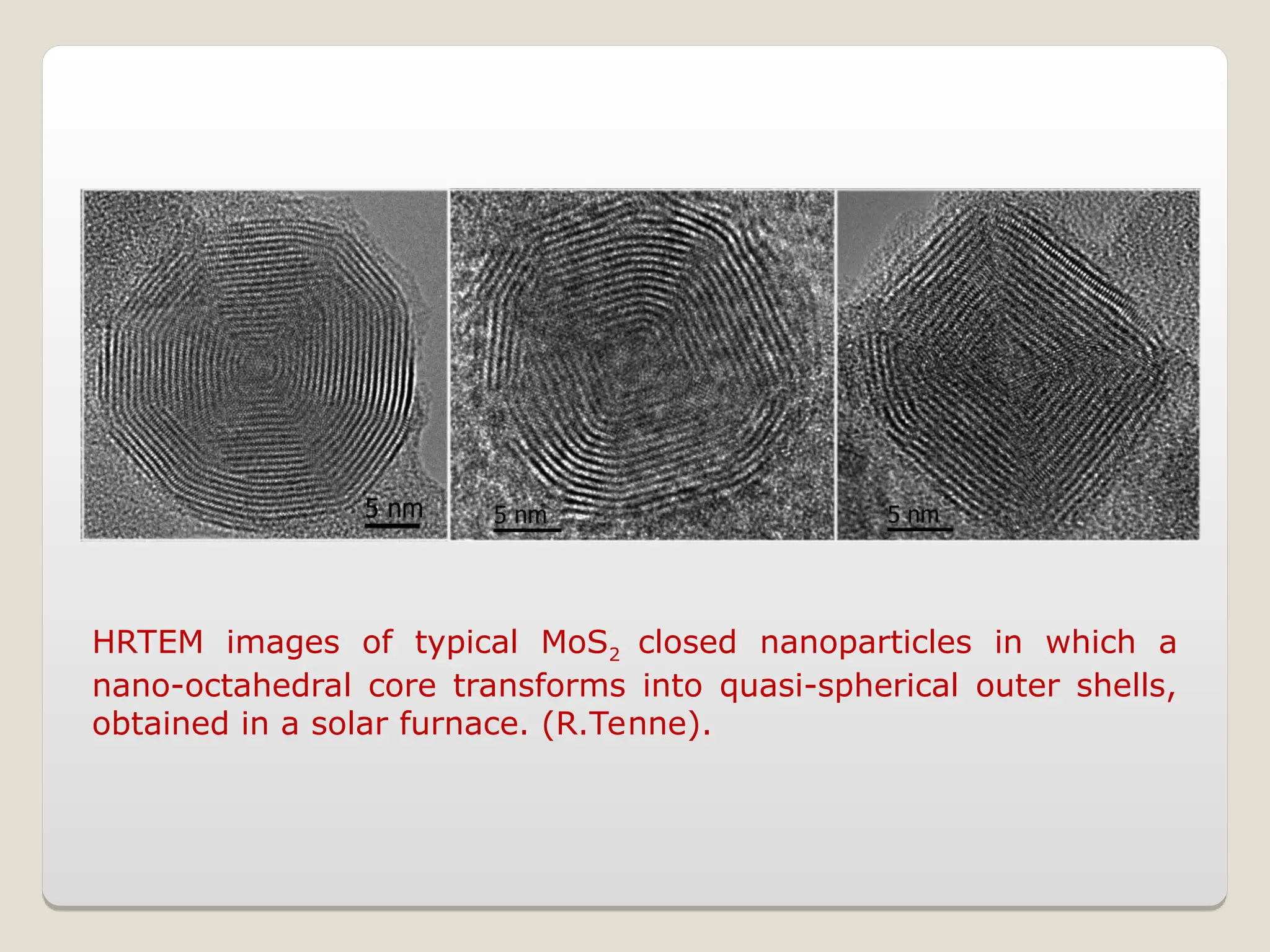
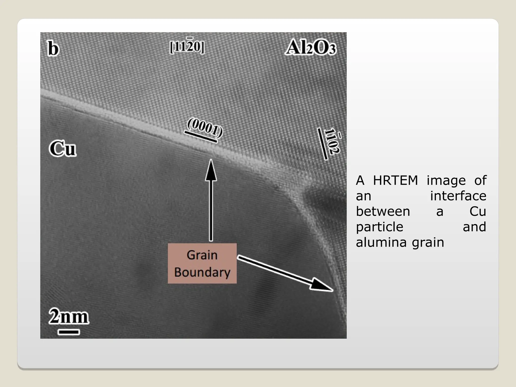
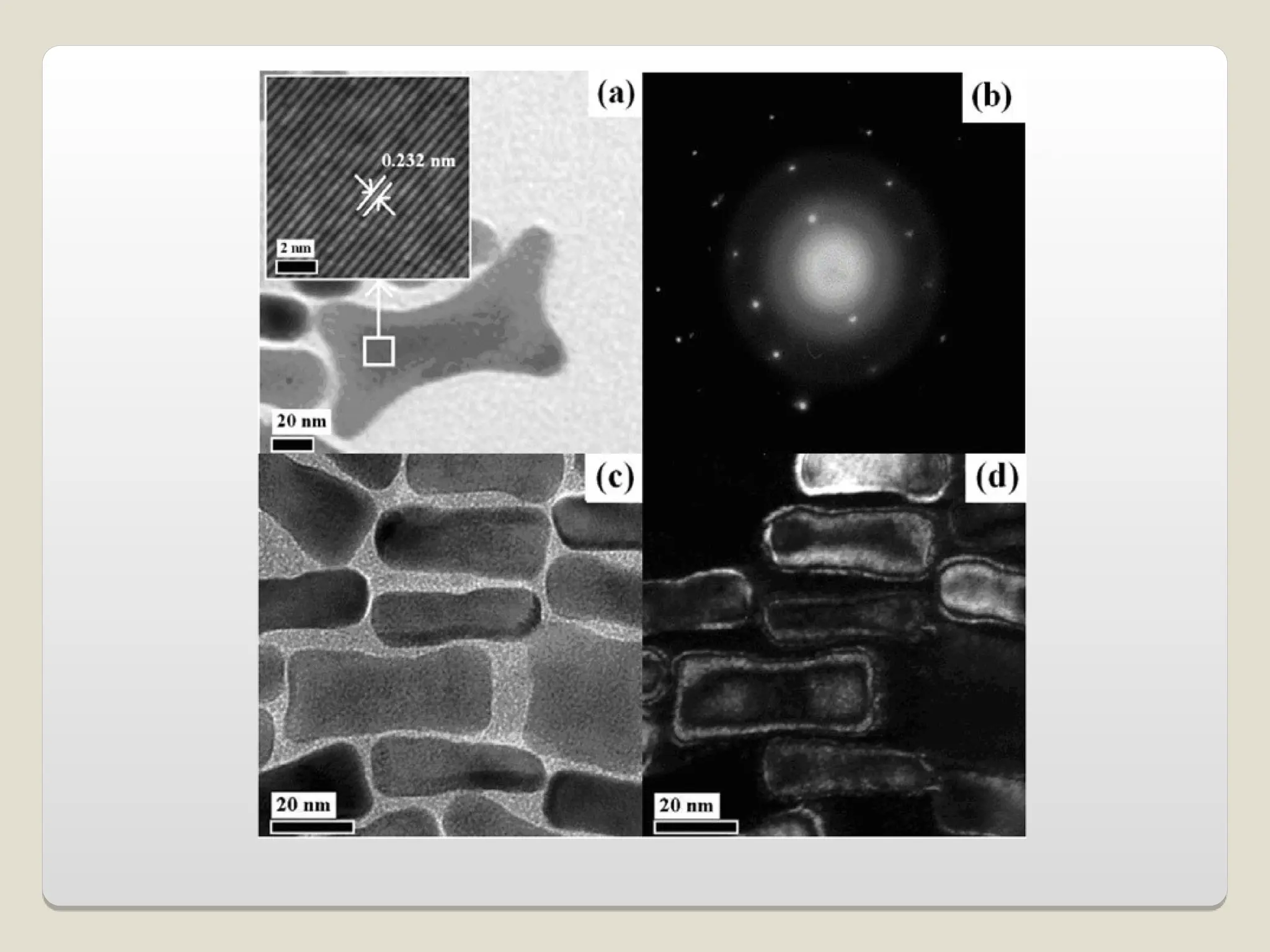
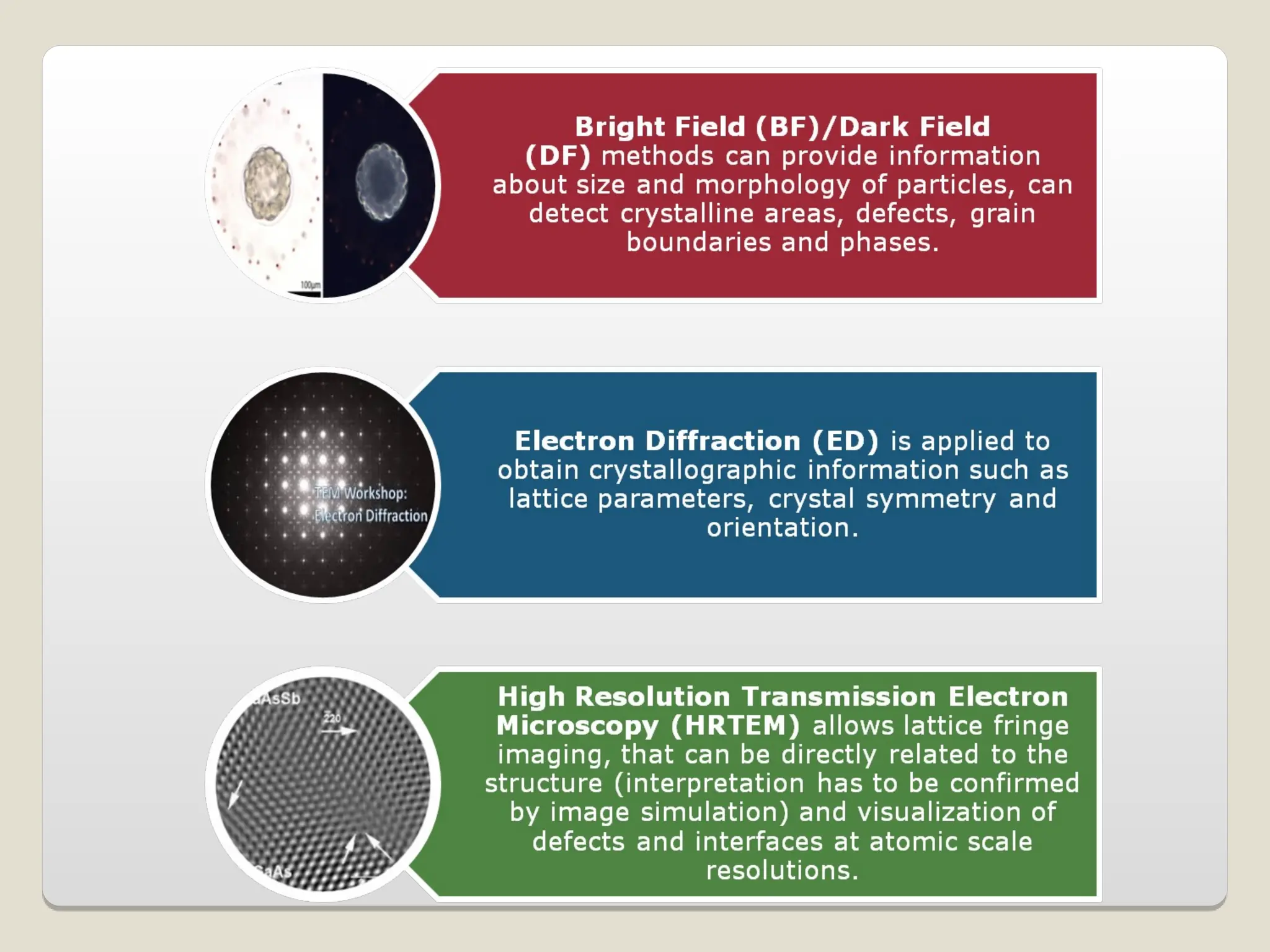
Transmission
Transmission
Electron
Electron
Microscopy
Microscopy
Transmission Electron Microscope (TEM)
Working Concept
TEM works much like a slide projector.
A projector shines a beam of light through (transmits) the
slide, as the light passes through it is affected by the structures
and objects on the slide.
These effects result in only certain parts of the light beam being
transmitted through certain parts of the slide.
This transmitted beam is then projected onto the viewing
screen, forming an enlarged image of the slide.
TEMs work the same way except that they shine a beam of
electrons (like the light) through the specimen (like the slide).
Whatever part is transmitted is projected onto a phosphor
screen for the user to see.
A more technical explanation of typical TEMs workings is as
follows
Transmission Electron
Microscopes
Scanning Electron
Microscopes
Detect transmitted electrons Detect scattered electrons
Accelerated Voltage >100 kV Accelerated voltage 20kV to
40kV
Thickness should not exceed
150 nm
Thickness is not important
Only small amount of sample
can be analysed at one time
Allows large amount of sample
to be analysed
Provide details about internal
composition
Focuses on sample surface and
composition
TEM
Interior
SEM
Surface
CLASSIFICATION OF TEM
•Conventional TEM
•High Resolution TEM
•Analytical Electron Microscopy
•Energy Filtering Electron Microscopy
•High Voltage Electron Microscopy
•Scanning TEM
Elasticity Scattered electrons
Source
Incident electrons that are scattered (deflected from their original
path) by atoms in the specimen in an elastic fashion (no loss of
energy).
These scattered electrons are then transmitted through the
remaining portions of the specimen
Utilization
•All electrons follow Bragg's Law and thus are scattered according to
Wavelength=2*Space between the atoms in the specimen*sin(angle of
scattering).
•All incident electrons have the same energy(thus wavelength) and enter
the specimen normal to its surface
•by adjusting the magnetic lenses such that the back focal plane of the lens
rather than the imaging plane is placed on the imaging apparatus a
diffraction pattern can be generated.
Specimen Interactions and utilization
Unscattered Electrons
Source
Incident electrons which are transmitted through
the thin specimen without any interaction occurring
inside the specimen.
Utilization
The transmission of unscattered electrons is inversely
proportional to the specimen thickness.
Areas of the specimen that are thicker will have fewer
transmitted unscattered electrons and so will appear darker,
conversely the thinner areas will have more transmitted and
thus will appear lighter.
These "similar angle" scattered electrons can be collated
using magnetic lenses to form a pattern of spots; each
spot corresponding to a specific atomic spacing (a
plane).
This pattern can then yield information about the
orientation, atomic arrangements and phases present in
the area being examined.
Topography
The surface features of an object or "how it looks", its texture; direct
relation between these features and materials properties (hardness,
reflectivity...etc.)
Morphology
The shape and size of the particles making up the object; direct
relation between these structures and materials properties (ductility,
strength, reactivity...etc.)
Composition
The elements and compounds that the object is composed of and the
relative amounts of them; direct relationship between composition
and materials properties (melting point, reactivity, hardness...etc.)
Crystallographic Information. How the atoms are arranged in the
object; direct relation between these arrangements and materials
properties (conductivity, electrical properties, strength...etc.)
•Very thin pieces are shaved
off using ultramicrotome filled
with a diamond, sapphire or
glass knife.
•Focussed ion beam is used to
etch away the undesired
portion of the sample. The
most common beam is gallium
ions with an energy of 30keV.
FOR NANOPARTICLES
STAINING
Staining involves the incorporation of high-atomic-number atoms into the polymer
to increase the density.
•It is used to enhance contrast to reveal details in multiphase polymers and in
composites with inorganic fillers.
•Stains may be applied directly to the specimen, to block faces produced by
microtomy, or to the sections themselves
•Most commonly used stains are osmium tetroxide and ruthenium tetroxide
•In positive staining, the region of interest is stained dark by either a chemical
interaction or selective physical absorption.
•In negative staining the shape of small particles mounted on smooth substrates is
shown by staining the regions surrounding the particles rather than the particles
themselves. It is often applied to latex or emulsion materials.
•Phases and crystal structure types
•Crystal symmetry and space group
•Orientation relationships between phases
•Determining growth directions, interface
coherency
•Identifying defects, i.e. twinning, SFs,
Dislocations
•Ordering behavior of crystal structures and
the site occupancy preferences
TEM Diffraction- What can we infer?
Bright field imaging
Only main beam is used. Aperture in back focal plane blocks
diffracted beams
Image contrast mainly due to subtraction of intensity from the
main beam by diffraction
In the bright field (BF) mode of the
TEM, an aperture is placed in the
back focal plane of the objective
lens which allows only the direct
beam to pass. In this case, the image
results from a weakening of the
direct beam by its interaction with
the sample. Therefore, mass-
thickness and
diffraction contrast contribute to
image formation: thick areas, areas
in which heavy atoms are enriched,
and crystalline areas appear with
dark contrast. It should be
mentioned that the interpretation of
images is often impeded by the
simultaneous occurence of the
contrast-forming phenomena.
Dark field imaging
Dark field imaging
Instead of main
beam, use a
diffracted beam
Move aperture to
diffracted beam
or tilt incident
beam
Dark-field microscopy (dark-ground
microscopy) describes microscopy
methods, in both light and electron
microscopy, which exclude the unscattered
beam from the image. As a result,
the field around the specimen (i.e., where
there is no specimen to scatter the beam)
is generally dark
Kikuchi lines
Kikuchi lines
θ
Inelastic
scattering
without
significant
wavelength
change leads to
formation of
Kikuchi lines by
diffraction.
Incoming beam
has every
possible
direction.
Outgoing strong
beam is at Bragg
angle. This is
particularly seen
in thick samples
Use Bragg’s law:  =
2dsin
But  much smaller
2  sin2 = R/L
=2dsin = d2
R = L(2)
Rd = L
Where L = camera
length
image plane
specimen
DIFFRACTION STUDIES
Ni2AlTi - P cubic
a = 2.92 Å
Cr23C6 - F cubic
a = 10.659 Å
Pattern of spots around transmitted beam from one grain
polycrystalline BaTiO3
spotty Debye rings
Polycrystalline Regions
•Detect epitaxy
•Orientation relationships at grain boundaries
•Orientation relationships between matrix & precipitates
•Determine directions of rapid growth
APPLICATIONS
Transmission electron microscopy (TEM) images
of silver nanoparticles with diameters of 20 nm
(a) TEM BF image of a cross-sectioned InAs/GaAs core-shell
nanowire. (b) DF image of the same nanowire with a bright contrast
in the shell region. (c) ED pattern of the same cross-sectioned
nanowire; the arrow indicated the reflection used to create the DF
image. (M. Heiblum and H. Shtrikman)
HRTEM images of typical MoS2 closed nanoparticles in which a
nano-octahedral core transforms into quasi-spherical outer shells,
obtained in a solar furnace. (R.Tenne).
A HRTEM image of
an interface
between a Cu
particle and
alumina grain
Transmission electron microscopy- Copy (2).ppt

Transmission electron microscopy- Copy (2).ppt

  • 1.
  • 3.
    Transmission Electron Microscope(TEM) Working Concept TEM works much like a slide projector. A projector shines a beam of light through (transmits) the slide, as the light passes through it is affected by the structures and objects on the slide. These effects result in only certain parts of the light beam being transmitted through certain parts of the slide. This transmitted beam is then projected onto the viewing screen, forming an enlarged image of the slide. TEMs work the same way except that they shine a beam of electrons (like the light) through the specimen (like the slide). Whatever part is transmitted is projected onto a phosphor screen for the user to see. A more technical explanation of typical TEMs workings is as follows
  • 6.
    Transmission Electron Microscopes Scanning Electron Microscopes Detecttransmitted electrons Detect scattered electrons Accelerated Voltage >100 kV Accelerated voltage 20kV to 40kV Thickness should not exceed 150 nm Thickness is not important Only small amount of sample can be analysed at one time Allows large amount of sample to be analysed Provide details about internal composition Focuses on sample surface and composition TEM Interior SEM Surface
  • 7.
    CLASSIFICATION OF TEM •ConventionalTEM •High Resolution TEM •Analytical Electron Microscopy •Energy Filtering Electron Microscopy •High Voltage Electron Microscopy •Scanning TEM
  • 8.
    Elasticity Scattered electrons Source Incidentelectrons that are scattered (deflected from their original path) by atoms in the specimen in an elastic fashion (no loss of energy). These scattered electrons are then transmitted through the remaining portions of the specimen Utilization •All electrons follow Bragg's Law and thus are scattered according to Wavelength=2*Space between the atoms in the specimen*sin(angle of scattering). •All incident electrons have the same energy(thus wavelength) and enter the specimen normal to its surface •by adjusting the magnetic lenses such that the back focal plane of the lens rather than the imaging plane is placed on the imaging apparatus a diffraction pattern can be generated.
  • 9.
    Specimen Interactions andutilization Unscattered Electrons Source Incident electrons which are transmitted through the thin specimen without any interaction occurring inside the specimen. Utilization The transmission of unscattered electrons is inversely proportional to the specimen thickness. Areas of the specimen that are thicker will have fewer transmitted unscattered electrons and so will appear darker, conversely the thinner areas will have more transmitted and thus will appear lighter.
  • 10.
    These "similar angle"scattered electrons can be collated using magnetic lenses to form a pattern of spots; each spot corresponding to a specific atomic spacing (a plane). This pattern can then yield information about the orientation, atomic arrangements and phases present in the area being examined.
  • 11.
    Topography The surface featuresof an object or "how it looks", its texture; direct relation between these features and materials properties (hardness, reflectivity...etc.) Morphology The shape and size of the particles making up the object; direct relation between these structures and materials properties (ductility, strength, reactivity...etc.) Composition The elements and compounds that the object is composed of and the relative amounts of them; direct relationship between composition and materials properties (melting point, reactivity, hardness...etc.) Crystallographic Information. How the atoms are arranged in the object; direct relation between these arrangements and materials properties (conductivity, electrical properties, strength...etc.)
  • 13.
    •Very thin piecesare shaved off using ultramicrotome filled with a diamond, sapphire or glass knife. •Focussed ion beam is used to etch away the undesired portion of the sample. The most common beam is gallium ions with an energy of 30keV.
  • 15.
  • 16.
    STAINING Staining involves theincorporation of high-atomic-number atoms into the polymer to increase the density. •It is used to enhance contrast to reveal details in multiphase polymers and in composites with inorganic fillers. •Stains may be applied directly to the specimen, to block faces produced by microtomy, or to the sections themselves •Most commonly used stains are osmium tetroxide and ruthenium tetroxide •In positive staining, the region of interest is stained dark by either a chemical interaction or selective physical absorption. •In negative staining the shape of small particles mounted on smooth substrates is shown by staining the regions surrounding the particles rather than the particles themselves. It is often applied to latex or emulsion materials.
  • 19.
    •Phases and crystalstructure types •Crystal symmetry and space group •Orientation relationships between phases •Determining growth directions, interface coherency •Identifying defects, i.e. twinning, SFs, Dislocations •Ordering behavior of crystal structures and the site occupancy preferences TEM Diffraction- What can we infer?
  • 20.
    Bright field imaging Brightfield imaging Only main beam is used. Aperture in back focal plane blocks diffracted beams Image contrast mainly due to subtraction of intensity from the main beam by diffraction
  • 21.
    In the brightfield (BF) mode of the TEM, an aperture is placed in the back focal plane of the objective lens which allows only the direct beam to pass. In this case, the image results from a weakening of the direct beam by its interaction with the sample. Therefore, mass- thickness and diffraction contrast contribute to image formation: thick areas, areas in which heavy atoms are enriched, and crystalline areas appear with dark contrast. It should be mentioned that the interpretation of images is often impeded by the simultaneous occurence of the contrast-forming phenomena.
  • 22.
    Dark field imaging Darkfield imaging Instead of main beam, use a diffracted beam Move aperture to diffracted beam or tilt incident beam
  • 23.
    Dark-field microscopy (dark-ground microscopy)describes microscopy methods, in both light and electron microscopy, which exclude the unscattered beam from the image. As a result, the field around the specimen (i.e., where there is no specimen to scatter the beam) is generally dark
  • 25.
    Kikuchi lines Kikuchi lines θ Inelastic scattering without significant wavelength changeleads to formation of Kikuchi lines by diffraction. Incoming beam has every possible direction. Outgoing strong beam is at Bragg angle. This is particularly seen in thick samples
  • 27.
    Use Bragg’s law: = 2dsin But  much smaller 2  sin2 = R/L =2dsin = d2 R = L(2) Rd = L Where L = camera length image plane specimen DIFFRACTION STUDIES
  • 29.
    Ni2AlTi - Pcubic a = 2.92 Å Cr23C6 - F cubic a = 10.659 Å Pattern of spots around transmitted beam from one grain
  • 30.
    polycrystalline BaTiO3 spotty Debyerings Polycrystalline Regions •Detect epitaxy •Orientation relationships at grain boundaries •Orientation relationships between matrix & precipitates •Determine directions of rapid growth
  • 31.
  • 32.
    Transmission electron microscopy(TEM) images of silver nanoparticles with diameters of 20 nm
  • 33.
    (a) TEM BFimage of a cross-sectioned InAs/GaAs core-shell nanowire. (b) DF image of the same nanowire with a bright contrast in the shell region. (c) ED pattern of the same cross-sectioned nanowire; the arrow indicated the reflection used to create the DF image. (M. Heiblum and H. Shtrikman)
  • 34.
    HRTEM images oftypical MoS2 closed nanoparticles in which a nano-octahedral core transforms into quasi-spherical outer shells, obtained in a solar furnace. (R.Tenne).
  • 36.
    A HRTEM imageof an interface between a Cu particle and alumina grain