FACULTY OF TECHNOLOGY &ENGINNERING
MATERIAL TECHNOLOGY
SCANNING TRANSMISSION ELECTRON
MICROSCOPE(STEM)
PRESANTED BY....
AKSHAY SAVANI
PRN NO-2017033800128346
NIKUNJ MANGUKIYA
PRN NO-2017033800128242
 Principle
 Construction
 Working
 Application
 Advantage
 Disadvantage
 Refrences
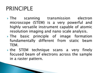
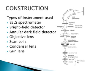
 The scanning transmission electron
microscope (STEM) is a very powerful and
highly versatile instrument capable of atomic
resolution imaging and nano scale analysis.
 The basic principle of image formation
fundamentally different from static beam
TEM.
 the STEM technique scans a very finely
focused beam of electrons across the sample
in a raster pattern.
Types of insterument used
 EELS spectrometer
 Bright-field detector
 Annular dark field detector
 Objective lens
 Scan coils
 Condenser lens
 Gun lens
 EELS spectrometer-As the electron beam
passes through the sample, some electrons in
the beam loss energy via inelastic scattering
interactions with electrons in the sample.
In electron energy loss spectroscopy (EELS),
the energy lost by the electrons in the beam
is measured using an electron spectrometer.
In STEM, EELS can be used to
spectroscopically map a sample at atomic
resolution
 Bright-field detector-In STEM, bright-field
detectors are located in the path of the
transmitted electron beam. Axial bright-field
detectors are located in the centre of the cone of
illumination of the transmitted beam, and are
often used to provide complementary images.
Annular bright-field detectors, located within the
cone of illumination of the transmitted beam,
have been used to obtain atomic resolution
images in which the atomic columns of light
elements such as oxygen are visible
 Annular dark field detector-In annular dark-
field mode, images are formed by fore-
scattered electrons incident on an annular
detector, which lies outside of the path of the
directly transmitted beam. By using a high-
angle ADF detector
 Scan coil-it is used for scanning the electron
beam across the specimen surface in a raster
pattern.
 Scan coils consist of to solenoids oriented in
a such a way to create two magnetic fields
perpendicular to each other.
 Condenser lens-if we want to focus the beam
to a size<10nm on the specimen surface the
magnification should be 1/5000 which is not
easily attained with one lens objective lens
only at that time condenser lens added to
demagnify the cross over point
 In many ways, the STEM is similar to the more
widely known scanning electron
microscope(SEM). An electron gun generates a
beam of electrons that is focused by a series of
lenses to form an image of the electron source at
a specimen. The electron spot, or probe, can be
scanned over the sample in a raster pattern by
exciting scanning deflection coils, and scattered
electrons are detected and their intensity plotted
as a function of probe position to form an image
 Scanning transmission electron microscopes are
used to characterize the nanoscale, and atomic
scale structure of specimens, providing
important insights into the properties and
behaviour of materials and biological cells.
 Materials science - Scanning transmission
electron microscopy has been applied to
characterize the structure of a wide range of
material specimens,
including semiconductor devices, complex
oxides, batteries, fuel cells, catalysts, and 2D
materials.
 Biology - The first application of STEM to the
imaging of biological molecules was
demonstrated in 1971
 STEM has been widely used to solve a number
of structural problems in molecular biology.
which can allow imaging of biological
samples without the need for staining
 Easy to operate with the proper training
 Advance in computer technology
 Insrument work fast
 It gives detailed in 3d and topografical
imaging and the versatile information
generated from different ditector
 It allows for the generation of data in digital
form
 Most sample require minimum preparation
action
 STEM are expensive and large.
 Special training require to operate STEM
 The preparation of samples can result in
artifacts
 Its limited to solid samples
 https://en.wikipedia.org/wiki/Scanning_trans
mission_electron_microscopy
 https://www.slideshare.net/e_gulfam/scanni
ng-transmission-electron-microscope
Thank
YOU

Stem

  • 2.
    FACULTY OF TECHNOLOGY&ENGINNERING MATERIAL TECHNOLOGY SCANNING TRANSMISSION ELECTRON MICROSCOPE(STEM) PRESANTED BY.... AKSHAY SAVANI PRN NO-2017033800128346 NIKUNJ MANGUKIYA PRN NO-2017033800128242
  • 3.
     Principle  Construction Working  Application  Advantage  Disadvantage  Refrences
  • 4.
     The scanningtransmission electron microscope (STEM) is a very powerful and highly versatile instrument capable of atomic resolution imaging and nano scale analysis.  The basic principle of image formation fundamentally different from static beam TEM.  the STEM technique scans a very finely focused beam of electrons across the sample in a raster pattern.
  • 5.
    Types of insterumentused  EELS spectrometer  Bright-field detector  Annular dark field detector  Objective lens  Scan coils  Condenser lens  Gun lens
  • 6.
     EELS spectrometer-Asthe electron beam passes through the sample, some electrons in the beam loss energy via inelastic scattering interactions with electrons in the sample. In electron energy loss spectroscopy (EELS), the energy lost by the electrons in the beam is measured using an electron spectrometer. In STEM, EELS can be used to spectroscopically map a sample at atomic resolution
  • 7.
     Bright-field detector-InSTEM, bright-field detectors are located in the path of the transmitted electron beam. Axial bright-field detectors are located in the centre of the cone of illumination of the transmitted beam, and are often used to provide complementary images. Annular bright-field detectors, located within the cone of illumination of the transmitted beam, have been used to obtain atomic resolution images in which the atomic columns of light elements such as oxygen are visible
  • 8.
     Annular darkfield detector-In annular dark- field mode, images are formed by fore- scattered electrons incident on an annular detector, which lies outside of the path of the directly transmitted beam. By using a high- angle ADF detector  Scan coil-it is used for scanning the electron beam across the specimen surface in a raster pattern.
  • 9.
     Scan coilsconsist of to solenoids oriented in a such a way to create two magnetic fields perpendicular to each other.  Condenser lens-if we want to focus the beam to a size<10nm on the specimen surface the magnification should be 1/5000 which is not easily attained with one lens objective lens only at that time condenser lens added to demagnify the cross over point
  • 10.
     In manyways, the STEM is similar to the more widely known scanning electron microscope(SEM). An electron gun generates a beam of electrons that is focused by a series of lenses to form an image of the electron source at a specimen. The electron spot, or probe, can be scanned over the sample in a raster pattern by exciting scanning deflection coils, and scattered electrons are detected and their intensity plotted as a function of probe position to form an image
  • 11.
     Scanning transmissionelectron microscopes are used to characterize the nanoscale, and atomic scale structure of specimens, providing important insights into the properties and behaviour of materials and biological cells.  Materials science - Scanning transmission electron microscopy has been applied to characterize the structure of a wide range of material specimens, including semiconductor devices, complex oxides, batteries, fuel cells, catalysts, and 2D materials.
  • 12.
     Biology -The first application of STEM to the imaging of biological molecules was demonstrated in 1971  STEM has been widely used to solve a number of structural problems in molecular biology. which can allow imaging of biological samples without the need for staining
  • 13.
     Easy tooperate with the proper training  Advance in computer technology  Insrument work fast  It gives detailed in 3d and topografical imaging and the versatile information generated from different ditector  It allows for the generation of data in digital form  Most sample require minimum preparation action
  • 14.
     STEM areexpensive and large.  Special training require to operate STEM  The preparation of samples can result in artifacts  Its limited to solid samples
  • 16.
  • 17.