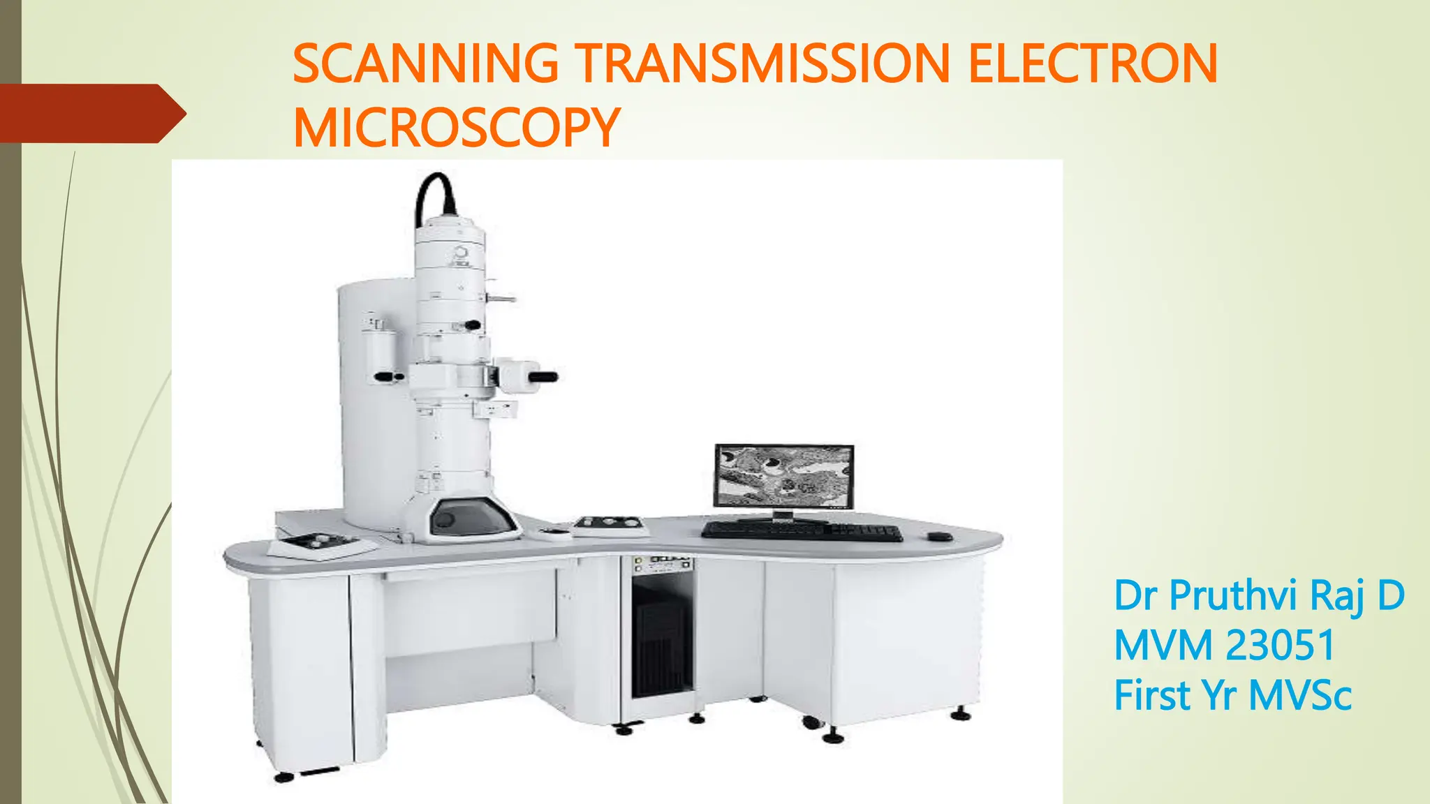
SCANNING TRANSMISSION ELECTRON
MICROSCOPY
Dr Pruthvi Raj D
MVM 23051
First Yr MVSc
TEM - images are formed by electrons passing through
a sufficiently thin specimen.
STEM - the electron beam is focused to a fine spot (with
the typical spot size 0.05 – 0.2 nm) which is then
scanned over the sample in a raster illumination system
constructed so that the sample is illuminated at each
point with the beam parallel to the optical axis.
RASTER PATTERN
Scanning transmission electron microscopy (STEM)
 Advanced imaging technique that is used to visualize
the structure and composition of materials at
nanometer to sub-atomic length scales.
 It provides high-resolution images
The Core Principle of STEM
 It scans a very finely focused beam of electrons across
the sample in a raster pattern.
 Interactions between the beam electrons and sample
atoms generate a serial signal stream.
 signal level at any location in the sample is represented
by the gray level at the corresponding location in the
image.
 Its primary advantage over conventional SEM imaging
is the improvement in spatial resolution.
Visualization journey
 Electron source - tungsten filament within Field
Emission Gun (FEG).
 Electron optical coloumn -The heart of the STEM
where electromagnetic lenses, such as condenser,
objective, and projector lenses, converge and steer
the electron beam with remarkable precision.
 Vacuum chamber -sample holder is the stage for
the specimen, allowing intricate manipulation across
multiple axes.
 The deflection coils, or scanners, are the essence of
the STEM's scanning capability. They meticulously
sweep the electron beam in a raster pattern over the
specimen, ensuring every segment is thoroughly
scanned.
 Detectors are the sentinels that capture the signals
from the electron beam after passing through
sample
 The Bright Field (BF) detector captures electrons that
have traversed the specimen with minimal deviation.
 Dark Field (DF) detectors, including the specialized
High-Angle Annular Dark Field (HAADF) variety, gather
electrons scattered at steep angles
 For surface detail, Secondary Electron (SE) detectors
offer topographical insights.
X ray microanalysis
 Electrons bombarding the specimen cause it to emit X-
rays whose energy is characteristic of the elemental
composition of the sample. It uses an energy dispersive
dispersive X-ray (EDX) spectrometer to count and sort
characteristic X-rays according to their energy.
 Wavelength dispersive X-ray (WDX) spectrometry
measures and counts X-rays by their wavelength (a
correlate of energy).
 Electron energy loss spectrometry (EELS) analyzes
transmitted electrons to determine the amount of
energy they have lost in interactions with the sample.
 It provides information about the interacting atoms,
including elemental identity, chemical bonding,
valence, conduction properties and surface
properties.
 Able to identify the element or specimen
SAMPLE PREPARATION FOR STEM
Fixation - fixed with chemical products (e.g.
glutaraldehyde)
Rinsing and 'staining" - treated with heavy metal
compounds.
Dehydration-washing with increasing ethanol
concentration, followed by final wash
Embedding in resin - material is gradually infiltrated with
the still unpolymerized resin.
Trimming of resin block and ultrathin sectioning -
sections with a thickness of about 70 nm are cut with
special knifes of cleaved glass. The cutting is done with a
ultra-microtome.
Specimen Thinning
Preparation done in two steps
1)Pre-Thinning:
Reducing the thickness to about 0.1mm
2)Final Thinning:
Reducing the thickness to about 100nm involve
 Ion Milling
 Electrolytic Thinning
 Ultramicrotomy
Ion Milling
Uses a beam of energetic ions to bombard specimen
surfaces to reduce the thickness by knocking atoms out of a
specimen
ion beam of 1-10 keV bombarded
specimen is placed in the center at certain angle
Electrolytic Thinning
Reducing specimen thickness to 100nm
A specimen placed in an electrochemical cell as anode
Common technique is jet polishinging
Electrolytic thinning completed in 3-15 minutes
Cryo-ultramicrotomy
 slicing the specimen at subzero temperatures to
preserve its native state and avert thermal degradation.
 solution for temperature-sensitive samples
 staining steps into the spotlight to enhance image
contrast.
 Biological specimens, inherently low in electron density,
density, benefit from the application of heavy metal
stains such as osmium, lead, uranium, or gold.
 These agents bind selectively to specific structures
within the sample, thereby increasing electron density
and enhancing contrast in the STEM imagery.
 The choice of stain hinges on the structures or
molecules of interest and the contrast required.
Typical STEM samples
tissue sections, lamella, and nanoparticles on the
order of 100 nm thickness or less, meet the criteria
for electron transparency.
Advantages
 Enabling the use of secondary electrons, scattered beam
electrons, characteristic X-rays, and electron energy loss
 High spatial resolution
 Non-destructive technique
 ability to image at much lower accelerating voltages to
prevent sample degradation.
Disadvantage
 STEM must be conducted in a vacuum so not suitable for
certain materials, particularly some biological samples,
which are not vacuum-compatible.
 The images produced are inherently monochrome and
thus tend to require a substantial level of interpretation.
Applications of STEM
It can provide sample’s physical structure, electronic
structure, and composition.
Biological sciences:
 Mass determination of macromolecules can be
precisely measured with HAADF imaging since the
HAADF signal is directly proportional to mass-thickness
 It has been most widely used for filamentous structures
like DNA.
 Both the ADF and HAADF signals can also be used to
visualize specific proteins that are labeled with heavy
atoms.
Electron tomography acquired in the STEM can yield 3D
reconstruction of cells and cell sections up to one
micrometer in thickness.
Ceramic grain boundaries: In the study of grain
boundaries in ceramics, the grain boundary character
significantly influences bulk materials properties such as
ionic conductivity.
Semiconductor interfaces: STEM is a major analytical
technique used in the semiconductor development
TEM STEM
Convergent Beam Parallel At certain angle
Magnification Post specimen intermediate lenses Detectors and digital imagfe software
References:
 https://lifesciences.danaher.com/us/en/products/microscope
s/topics/scanning-transmission-electron-microscopy.html
 https://search.app.goo.gl/P3Necxf
 https://measurlabs.com/methods/scanning-transmission-
electron-microscopy/
THANK YOU

Scanning transmission electron microscopy

  • 1.
    SCANNING TRANSMISSION ELECTRON MICROSCOPY DrPruthvi Raj D MVM 23051 First Yr MVSc
  • 2.
    TEM - imagesare formed by electrons passing through a sufficiently thin specimen. STEM - the electron beam is focused to a fine spot (with the typical spot size 0.05 – 0.2 nm) which is then scanned over the sample in a raster illumination system constructed so that the sample is illuminated at each point with the beam parallel to the optical axis.
  • 4.
  • 5.
    Scanning transmission electronmicroscopy (STEM)  Advanced imaging technique that is used to visualize the structure and composition of materials at nanometer to sub-atomic length scales.  It provides high-resolution images
  • 6.
    The Core Principleof STEM  It scans a very finely focused beam of electrons across the sample in a raster pattern.  Interactions between the beam electrons and sample atoms generate a serial signal stream.  signal level at any location in the sample is represented by the gray level at the corresponding location in the image.  Its primary advantage over conventional SEM imaging is the improvement in spatial resolution.
  • 7.
    Visualization journey  Electronsource - tungsten filament within Field Emission Gun (FEG).  Electron optical coloumn -The heart of the STEM where electromagnetic lenses, such as condenser, objective, and projector lenses, converge and steer the electron beam with remarkable precision.
  • 9.
     Vacuum chamber-sample holder is the stage for the specimen, allowing intricate manipulation across multiple axes.  The deflection coils, or scanners, are the essence of the STEM's scanning capability. They meticulously sweep the electron beam in a raster pattern over the specimen, ensuring every segment is thoroughly scanned.  Detectors are the sentinels that capture the signals from the electron beam after passing through sample
  • 10.
     The BrightField (BF) detector captures electrons that have traversed the specimen with minimal deviation.  Dark Field (DF) detectors, including the specialized High-Angle Annular Dark Field (HAADF) variety, gather electrons scattered at steep angles  For surface detail, Secondary Electron (SE) detectors offer topographical insights.
  • 13.
    X ray microanalysis Electrons bombarding the specimen cause it to emit X- rays whose energy is characteristic of the elemental composition of the sample. It uses an energy dispersive dispersive X-ray (EDX) spectrometer to count and sort characteristic X-rays according to their energy.  Wavelength dispersive X-ray (WDX) spectrometry measures and counts X-rays by their wavelength (a correlate of energy).  Electron energy loss spectrometry (EELS) analyzes transmitted electrons to determine the amount of energy they have lost in interactions with the sample.
  • 14.
     It providesinformation about the interacting atoms, including elemental identity, chemical bonding, valence, conduction properties and surface properties.  Able to identify the element or specimen
  • 15.
    SAMPLE PREPARATION FORSTEM Fixation - fixed with chemical products (e.g. glutaraldehyde) Rinsing and 'staining" - treated with heavy metal compounds. Dehydration-washing with increasing ethanol concentration, followed by final wash Embedding in resin - material is gradually infiltrated with the still unpolymerized resin. Trimming of resin block and ultrathin sectioning - sections with a thickness of about 70 nm are cut with special knifes of cleaved glass. The cutting is done with a ultra-microtome.
  • 16.
    Specimen Thinning Preparation donein two steps 1)Pre-Thinning: Reducing the thickness to about 0.1mm 2)Final Thinning: Reducing the thickness to about 100nm involve  Ion Milling  Electrolytic Thinning  Ultramicrotomy
  • 17.
    Ion Milling Uses abeam of energetic ions to bombard specimen surfaces to reduce the thickness by knocking atoms out of a specimen ion beam of 1-10 keV bombarded specimen is placed in the center at certain angle Electrolytic Thinning Reducing specimen thickness to 100nm A specimen placed in an electrochemical cell as anode Common technique is jet polishinging Electrolytic thinning completed in 3-15 minutes
  • 19.
    Cryo-ultramicrotomy  slicing thespecimen at subzero temperatures to preserve its native state and avert thermal degradation.  solution for temperature-sensitive samples  staining steps into the spotlight to enhance image contrast.  Biological specimens, inherently low in electron density, density, benefit from the application of heavy metal stains such as osmium, lead, uranium, or gold.  These agents bind selectively to specific structures within the sample, thereby increasing electron density and enhancing contrast in the STEM imagery.  The choice of stain hinges on the structures or molecules of interest and the contrast required.
  • 20.
    Typical STEM samples tissuesections, lamella, and nanoparticles on the order of 100 nm thickness or less, meet the criteria for electron transparency.
  • 21.
    Advantages  Enabling theuse of secondary electrons, scattered beam electrons, characteristic X-rays, and electron energy loss  High spatial resolution  Non-destructive technique  ability to image at much lower accelerating voltages to prevent sample degradation. Disadvantage  STEM must be conducted in a vacuum so not suitable for certain materials, particularly some biological samples, which are not vacuum-compatible.  The images produced are inherently monochrome and thus tend to require a substantial level of interpretation.
  • 22.
    Applications of STEM Itcan provide sample’s physical structure, electronic structure, and composition. Biological sciences:  Mass determination of macromolecules can be precisely measured with HAADF imaging since the HAADF signal is directly proportional to mass-thickness  It has been most widely used for filamentous structures like DNA.  Both the ADF and HAADF signals can also be used to visualize specific proteins that are labeled with heavy atoms.
  • 23.
    Electron tomography acquiredin the STEM can yield 3D reconstruction of cells and cell sections up to one micrometer in thickness. Ceramic grain boundaries: In the study of grain boundaries in ceramics, the grain boundary character significantly influences bulk materials properties such as ionic conductivity. Semiconductor interfaces: STEM is a major analytical technique used in the semiconductor development
  • 24.
    TEM STEM Convergent BeamParallel At certain angle Magnification Post specimen intermediate lenses Detectors and digital imagfe software
  • 25.
  • 26.