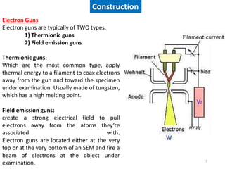
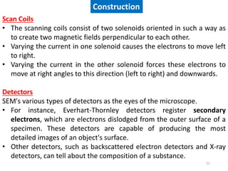
SCANNING ELECTRON MICROSCOPE (SEM)
1
Introduction
• A scanning electron microscope (SEM) is a type of electron
microscope that produces images of a sample by scanning the surface
with a focused beam of electrons.
• The electrons interact with atoms in the sample, producing various
signals that contain information about the sample's surface
topography and composition.
• It can obtain high magnification images, with a good depth of field.
• It can also analyze individual crystals or other features. A high-
resolution SEM image can show detail down to 25 Angstroms, or
better.
• When used in conjunction with the closely-related technique of
energy-dispersive X-ray microanalysis (EDX, EDS, EDAX), the
composition of individual crystals or features can be determined.2
Applications
• SEMs have a variety of applications in a number of scientific and
industry-related fields, especially where characterizations of solid
materials is beneficial.
• In addition to topographical, morphological and compositional
information, a Scanning Electron Microscope can detect and analyze
surface fractures, provide information in microstructures, examine
surface contaminations, reveal spatial variations in chemical
compositions, provide qualitative chemical analyses and identify
crystalline structures.
• In addition, SEMs have practical industrial and technological
applications such as semiconductor inspection, production line of
miniscule products and assembly of microchips for computers.
• SEMs can be as essential research tool in fields such as life science,
biology, gemology, medical and forensic science, metallurgy. 3
SEM vs complementary techniques
• Optical microscopy limited by wavelength of visible
light. However, very simple and larger areas can be seen.
• AFM limited by smaller scan areas than SEM. Limited to
relatively “smoother” surfaces. However, is quantitative.
• SEM is more qualitative. However, rapid and easy
assessment of chemistry and topography at “~ 1” nm
length scales. Large depth of focus.
4
Principle
5
• The basic principle is that a beam of electrons is generated
by a suitable source, typically a tungsten filament or a field
emission gun.
• The electron beam is accelerated through a high voltage
(e.g.: 20 kV) and pass through a system of apertures and
electromagnetic lenses to produce a thin beam of electrons.
• Then the beam scans the surface of the specimen. Electrons
are emitted from the specimen by the action of the
scanning beam and collected by a suitably positioned
detector.
Construction
6
Scanning Electron Microscope
’s basic components are as
following…
• Electron gun (Filament)
• Condenser lenses
• Objective Aperture
• Scan coils
• Chamber (specimen test)
• Detectors
• Computer hardware and software
Construction
7
Electron Guns
Electron guns are typically of TWO types.
1) Thermionic guns
2) Field emission guns
Thermionic guns:
Which are the most common type, apply
thermal energy to a filament to coax electrons
away from the gun and toward the specimen
under examination. Usually made of tungsten,
which has a high melting point.
Field emission guns:
create a strong electrical field to pull
electrons away from the atoms they‘re
associated with.
Electron guns are located either at the very
top or at the very bottom of an SEM and fire a
beam of electrons at the object under
examination.
Construction
8
Condenser Lenses
• Just like optical microscopes, SEMs use Condenser lenses to produce
clear and detailed images.
• The Condenser lenses in these devices, however, work differently. For
one thing, they aren't made of glass.
• Instead, the Condenser lenses are made of magnets capable of
bending the path of electrons.
• By doing so, the Condenser lenses focus and control the electron
beam, ensuring that the electrons end up precisely where they need
to go.
Construction
9
Objective Aperture
The objective aperture arm fits above
the objective lens in the SEM. It is a
metal rod that holds a thin plate of metal
containing four holes. Over this fits a
much thinner rectangle of metal with
holes (apertures) of different sizes. By
moving the arm in and out different sized
holes can be put into the beam path.
Construction
10
Scan Coils
• The scanning coils consist of two solenoids oriented in such a way as
to create two magnetic fields perpendicular to each other.
• Varying the current in one solenoid causes the electrons to move left
to right.
• Varying the current in the other solenoid forces these electrons to
move at right angles to this direction (left to right) and downwards.
Detectors
SEM's various types of detectors as the eyes of the microscope.
• For instance, Everhart-Thornley detectors register secondary
electrons, which are electrons dislodged from the outer surface of a
specimen. These detectors are capable of producing the most
detailed images of an object's surface.
• Other detectors, such as backscattered electron detectors and X-ray
detectors, can tell about the composition of a substance.
Construction
11
Scan Coils
• The scanning coils consist of two solenoids oriented in such a way as
to create two magnetic fields perpendicular to each other.
• Varying the current in one solenoid causes the electrons to move left
to right.
• Varying the current in the other solenoid forces these electrons to
move at right angles to this direction (left to right) and downwards.
Detectors
SEM's various types of detectors as the eyes of the microscope.
• For instance, Everhart-Thornley detectors register secondary
electrons, which are electrons dislodged from the outer surface of a
specimen. These detectors are capable of producing the most
detailed images of an object's surface.
• Other detectors, such as backscattered electron detectors and X-ray
detectors, can tell about the composition of a substance.
Construction
12
Vacuum Chamber
SEMs require a vacuum to operate.
• Without a vacuum, the electron beam generated by the electron gun
would encounter constant interference from air particles in the
atmosphere.
• Not only would these particles block the path of the electron beam,
they would also be knocked out of the air and onto the specimen,
which would distort the surface of the specimen.
13
14
Signals coming out from the interaction
volume
15
The Signals:
SE and BSE
+
++
++
+
16
X-rays
+
++
++
+
X-Ray
17
Auger Electrons
+
X-Ray
Auger
Electron
18
• Back Scattered Electrons (Atomic number contrast,
topographic contrast, channelling contrast)
• Secondary Electrons (Topographic Contrast)
• X-rays (EDAX Chem Composition)
• Photons (Cathodoluminiscence)
• Auger Electrons (Surface Compositional Analysis)
19
BSE and SE: Yields
Yield = Number of electrons emitted
Number of incident electrons
This number is responsible for contrast in SEM images along
with trajectory and energy.
Yield is affected by atomic number, kV, specimen tilt.
20
Aberrations in SEM
Rays further from the optical axis are focussed closer to the
lens resulting in an aberration disc:
Lens
a
Spherical Aberration
21
Aberrations
The focal length depends on the electron energy.
An energy spread of the electrons result in an aberration disc:
Lens
a
E=E0
E=E0-DE
Chromatic Aberration
22
Aberrations
Astigmatism
e-
Due to lens inhomogeneities electrons diverging from a single
point P will, after aberrations, produce two separate line foci at
right angles to each other
P
Astigmatism is corrected by a stigmator that forces the two
separate line foci to fall on a single plane.
Astigmatism causes image
distortion
23
Imaging non-conductors
• The goal is to avoid implanting charge deep
beneath the surface. If this is allowed to occur
then stable imaging may never be achieved.
• Step #1 - Set the SEM
to the lowest operating
energy
• If the sample is charging positive (i.e. a dark scan
square) Increase the beam energy and proceed to
image
• If sample is charging negatively (i.e. bright scan
square), Since we cannot reduce E any further go
on to step 3.
• Step #2 - Determine the
charging state of the
sample using the scan
square test
Step 3
Tilt the sample to 45 degrees and repeat the
usual scan square test
Tilting the sample reduces charging at all
energies
24
If all else fails…..coat a thin layer of metal (5nm of
Au/Pd, 2nm of Cr) on the sample
• Coatings do not make the sample a
conductor
• They form a ground plane - i.e. the
free electrons in the metal move so as
to eliminate the external field
• The charge is not eliminated but the
disruptive field is removed
25
Disadvantages
• The disadvantages of a Scanning Electron Microscope start with the
size and cost. SEMs are expensive, large and must be housed in an
area free of any possible electric, magnetic or vibration interference.
• Maintenance involves keeping a steady voltage, currents to
electromagnetic coils and circulation of cool water.
• SEMs are limited to solid, inorganic samples small enough to fit inside
the vacuum chamber that can handle moderate vacuum pressure.
Thank you

Sem

  • 1.
  • 2.
    Introduction • A scanningelectron microscope (SEM) is a type of electron microscope that produces images of a sample by scanning the surface with a focused beam of electrons. • The electrons interact with atoms in the sample, producing various signals that contain information about the sample's surface topography and composition. • It can obtain high magnification images, with a good depth of field. • It can also analyze individual crystals or other features. A high- resolution SEM image can show detail down to 25 Angstroms, or better. • When used in conjunction with the closely-related technique of energy-dispersive X-ray microanalysis (EDX, EDS, EDAX), the composition of individual crystals or features can be determined.2
  • 3.
    Applications • SEMs havea variety of applications in a number of scientific and industry-related fields, especially where characterizations of solid materials is beneficial. • In addition to topographical, morphological and compositional information, a Scanning Electron Microscope can detect and analyze surface fractures, provide information in microstructures, examine surface contaminations, reveal spatial variations in chemical compositions, provide qualitative chemical analyses and identify crystalline structures. • In addition, SEMs have practical industrial and technological applications such as semiconductor inspection, production line of miniscule products and assembly of microchips for computers. • SEMs can be as essential research tool in fields such as life science, biology, gemology, medical and forensic science, metallurgy. 3
  • 4.
    SEM vs complementarytechniques • Optical microscopy limited by wavelength of visible light. However, very simple and larger areas can be seen. • AFM limited by smaller scan areas than SEM. Limited to relatively “smoother” surfaces. However, is quantitative. • SEM is more qualitative. However, rapid and easy assessment of chemistry and topography at “~ 1” nm length scales. Large depth of focus. 4
  • 5.
    Principle 5 • The basicprinciple is that a beam of electrons is generated by a suitable source, typically a tungsten filament or a field emission gun. • The electron beam is accelerated through a high voltage (e.g.: 20 kV) and pass through a system of apertures and electromagnetic lenses to produce a thin beam of electrons. • Then the beam scans the surface of the specimen. Electrons are emitted from the specimen by the action of the scanning beam and collected by a suitably positioned detector.
  • 6.
    Construction 6 Scanning Electron Microscope ’sbasic components are as following… • Electron gun (Filament) • Condenser lenses • Objective Aperture • Scan coils • Chamber (specimen test) • Detectors • Computer hardware and software
  • 7.
    Construction 7 Electron Guns Electron gunsare typically of TWO types. 1) Thermionic guns 2) Field emission guns Thermionic guns: Which are the most common type, apply thermal energy to a filament to coax electrons away from the gun and toward the specimen under examination. Usually made of tungsten, which has a high melting point. Field emission guns: create a strong electrical field to pull electrons away from the atoms they‘re associated with. Electron guns are located either at the very top or at the very bottom of an SEM and fire a beam of electrons at the object under examination.
  • 8.
    Construction 8 Condenser Lenses • Justlike optical microscopes, SEMs use Condenser lenses to produce clear and detailed images. • The Condenser lenses in these devices, however, work differently. For one thing, they aren't made of glass. • Instead, the Condenser lenses are made of magnets capable of bending the path of electrons. • By doing so, the Condenser lenses focus and control the electron beam, ensuring that the electrons end up precisely where they need to go.
  • 9.
    Construction 9 Objective Aperture The objectiveaperture arm fits above the objective lens in the SEM. It is a metal rod that holds a thin plate of metal containing four holes. Over this fits a much thinner rectangle of metal with holes (apertures) of different sizes. By moving the arm in and out different sized holes can be put into the beam path.
  • 10.
    Construction 10 Scan Coils • Thescanning coils consist of two solenoids oriented in such a way as to create two magnetic fields perpendicular to each other. • Varying the current in one solenoid causes the electrons to move left to right. • Varying the current in the other solenoid forces these electrons to move at right angles to this direction (left to right) and downwards. Detectors SEM's various types of detectors as the eyes of the microscope. • For instance, Everhart-Thornley detectors register secondary electrons, which are electrons dislodged from the outer surface of a specimen. These detectors are capable of producing the most detailed images of an object's surface. • Other detectors, such as backscattered electron detectors and X-ray detectors, can tell about the composition of a substance.
  • 11.
    Construction 11 Scan Coils • Thescanning coils consist of two solenoids oriented in such a way as to create two magnetic fields perpendicular to each other. • Varying the current in one solenoid causes the electrons to move left to right. • Varying the current in the other solenoid forces these electrons to move at right angles to this direction (left to right) and downwards. Detectors SEM's various types of detectors as the eyes of the microscope. • For instance, Everhart-Thornley detectors register secondary electrons, which are electrons dislodged from the outer surface of a specimen. These detectors are capable of producing the most detailed images of an object's surface. • Other detectors, such as backscattered electron detectors and X-ray detectors, can tell about the composition of a substance.
  • 12.
    Construction 12 Vacuum Chamber SEMs requirea vacuum to operate. • Without a vacuum, the electron beam generated by the electron gun would encounter constant interference from air particles in the atmosphere. • Not only would these particles block the path of the electron beam, they would also be knocked out of the air and onto the specimen, which would distort the surface of the specimen.
  • 13.
  • 14.
    14 Signals coming outfrom the interaction volume
  • 15.
  • 16.
  • 17.
  • 18.
    18 • Back ScatteredElectrons (Atomic number contrast, topographic contrast, channelling contrast) • Secondary Electrons (Topographic Contrast) • X-rays (EDAX Chem Composition) • Photons (Cathodoluminiscence) • Auger Electrons (Surface Compositional Analysis)
  • 19.
    19 BSE and SE:Yields Yield = Number of electrons emitted Number of incident electrons This number is responsible for contrast in SEM images along with trajectory and energy. Yield is affected by atomic number, kV, specimen tilt.
  • 20.
    20 Aberrations in SEM Raysfurther from the optical axis are focussed closer to the lens resulting in an aberration disc: Lens a Spherical Aberration
  • 21.
    21 Aberrations The focal lengthdepends on the electron energy. An energy spread of the electrons result in an aberration disc: Lens a E=E0 E=E0-DE Chromatic Aberration
  • 22.
    22 Aberrations Astigmatism e- Due to lensinhomogeneities electrons diverging from a single point P will, after aberrations, produce two separate line foci at right angles to each other P Astigmatism is corrected by a stigmator that forces the two separate line foci to fall on a single plane. Astigmatism causes image distortion
  • 23.
    23 Imaging non-conductors • Thegoal is to avoid implanting charge deep beneath the surface. If this is allowed to occur then stable imaging may never be achieved. • Step #1 - Set the SEM to the lowest operating energy • If the sample is charging positive (i.e. a dark scan square) Increase the beam energy and proceed to image • If sample is charging negatively (i.e. bright scan square), Since we cannot reduce E any further go on to step 3. • Step #2 - Determine the charging state of the sample using the scan square test Step 3 Tilt the sample to 45 degrees and repeat the usual scan square test Tilting the sample reduces charging at all energies
  • 24.
    24 If all elsefails…..coat a thin layer of metal (5nm of Au/Pd, 2nm of Cr) on the sample • Coatings do not make the sample a conductor • They form a ground plane - i.e. the free electrons in the metal move so as to eliminate the external field • The charge is not eliminated but the disruptive field is removed
  • 25.
    25 Disadvantages • The disadvantagesof a Scanning Electron Microscope start with the size and cost. SEMs are expensive, large and must be housed in an area free of any possible electric, magnetic or vibration interference. • Maintenance involves keeping a steady voltage, currents to electromagnetic coils and circulation of cool water. • SEMs are limited to solid, inorganic samples small enough to fit inside the vacuum chamber that can handle moderate vacuum pressure. Thank you