Downloaded 3,042 times

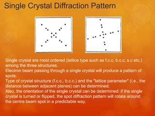
![EXAMPLE OF DIFFRACTION PATTERN
In this case incident beam direction B [100] in an Aluminum (f,c.c),
single crystal specimen. Transmitted beam is marked as T and the
arrangement of the diffracted beams D around the transmitted beam
is the characteristic of the four fold symmetry of the [100] cube axis
of Aluminum.](https://image.slidesharecdn.com/semandtem-131031222830-phpapp02/85/Sem-and-tem-17-320.jpg)
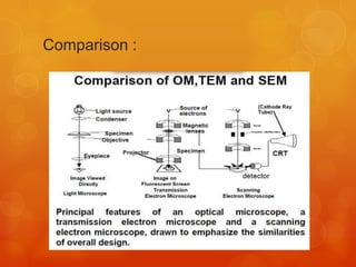

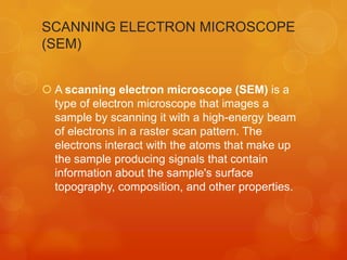
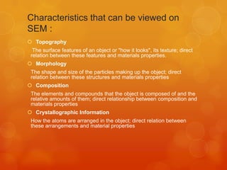
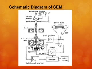
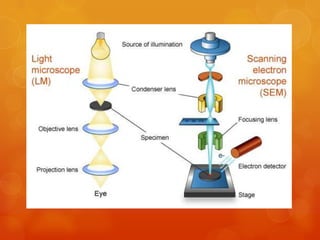
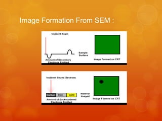
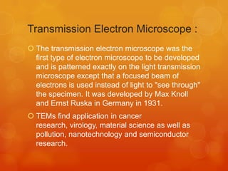
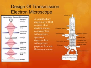
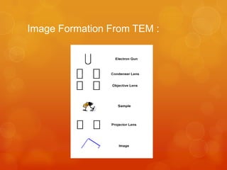
Scanning electron microscopes (SEM) and transmission electron microscopes (TEM) were developed to overcome limitations of light microscopes and enable higher magnification. SEM uses a focused beam of electrons to scan sample surfaces, revealing topography, composition, and other properties. TEM transmits electrons through thin samples to form magnified images and diffraction patterns, allowing visualization of structures like organelles and crystal structures. While both use electron beams, SEM analyzes surface features and TEM transmits through samples, giving each technique different applications and resolution capabilities.