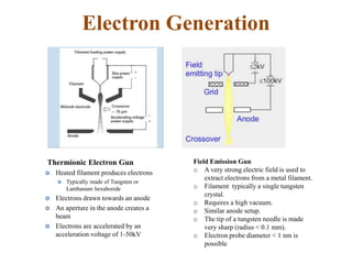
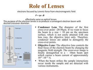
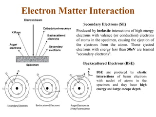
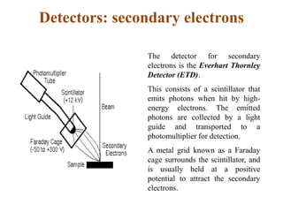
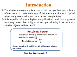
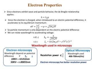
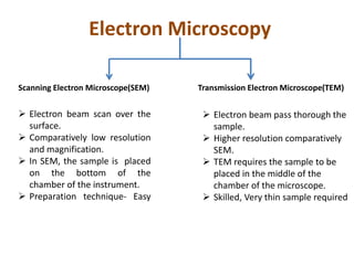
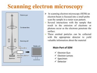
The document summarizes electron microscopy. It describes how electron microscopy works by using a beam of electrons instead of light to image specimens. It discusses the main components of a scanning electron microscope, including the electron gun, electron lenses, and detectors. It also explains how scanning electron microscopes function by scanning a focused electron beam over a sample to produce signals containing information about the sample's surface topography and composition.
![How an Electron Beam is Produced?
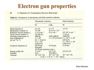
• Electron guns are used to produce a fine, controlled beam of
electrons which are then focused at the specimen surface.
• The electron guns may either be
(1) Thermionic gun or
(2) field-emission gun.
Cathode current density (emission current density)
For Thermionic emission
Richardson Law:
Jc = AcT2exp(-Ew/kT) in A/cm2
For Tungsten: T = 2700K Work function Ew = 4.5ev
Jc = 3.4 A/cm2
Improve current density?
Use cathode material of lower Ew
For LaB6 single crystal T=1700K
Work function Ew=2.7ev
Jc = 25 A/cm2
Brightness
[Β = 4ip / (π dp αp)2]
W filament
LaB6 Single
Crystal αp Probe convergence
angle.
dp Probe diameter or
spot size.
ip Probe current
The resolution is determined by beam
diameter.](https://image.slidesharecdn.com/electronmicroscopynpiu5-180201120356/85/Scanning-Electron-microscopy-7-320.jpg)