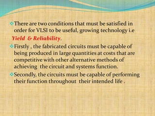
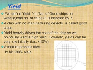
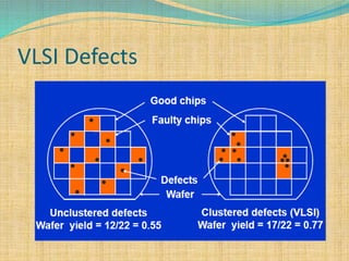
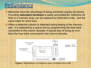
There are two key requirements for VLSI memory to be useful: yield and reliability. Yield refers to the percentage of good chips produced, which impacts costs. Reliability means the memory performs as intended for a given period of time under conditions. As integration density increases, yield decreases due to defects and variations. Memory designers use redundancy and error correction to combat this. Redundancy replaces defective components like columns or rows. Error correction adds redundant data bits to detect and fix errors. This improves yield and addresses soft errors.
This presentation discusses the Lambda based design rules for drawing the layouts. The spacing between ltwo layers, extent if of overlap, minimum dimensions of each layer etc are decided by the lambda based design rules. the separation between metal and poly, poly and diffusion , width of metal etc
TYPES OF PLACEMENT,GOOD PLACEMENT VS. BAD PLACEMENT ,ALGORITHMS, ASIC DESIGN FLOW DIAGRAM,DEFINITION OF PLACEMENT,TECHNIQUES USED FOR PLACEMENT,PLACEMENT TRENDS,SOLUTIONS
I have prepared it to create an understanding of delay modeling in VLSI.
Regards,
Vishal Sharma
Doctoral Research Scholar,
IIT Indore
vishalfzd@gmail.com
Low Power VLSI design architecture for EDA (Electronic Design Automation) and Modern Power Estimation, Reduction and Fixing technologies including clock gating and power gating
World's First Intel® Thunderbolt™ 3 Certified Motherboard
Supports 6th Generation Intel® Core™ Processor
Dual Channel DDR4, 4 DIMMs
Thunderbolt™ 3 brings Thunderbolt to USB Type-C™ at speeds up to 40 Gbps
Intel® USB 3.1 with USB Type-C™ support Power Delivery 2.0 for up to 36W
3-Way Graphics Support with Exclusive Ultra Durable Metal Shielding over the PCIe Slots
PCIe Gen3 x4 M.2 Connector with up to 32Gb/s Data Transfer (PCIe NVMe & SATA SSD support)
3 SATA Express Connectors for up to 16Gb/s Data Transfer
HDMI 2.0 for 4K@60Hz and 21:9 aspect ratio provide the finest viewing experience
115dB SNR HD Audio with Built-in Rear Audio Amplifier
High Quality Audio Capacitors and Audio Noise Guard with LED Trace Path Lighting
Intel® GbE LAN with cFosSpeed Internet Accelerator Software
Gold Plating for CPU Socket, Memory DIMMs with 2X Copper PCB
APP Center Including EasyTune™ and Cloud Station™ Utilities
GIGABYTE UEFI DualBIOS™ Technology
Average and Static Power Analysis of a 6T and 7T SRAM Bit-Cell at 180nm, 90nm...idescitation
A lot of consideration has been given to problems arising due to power dissipation.
Different ideas have been proposed by many researchers from the device level to the
architectural level and above. However, there is no universal way to avoid tradeoffs between
the power, delay and area. This is why; the designers are required to choose appropriate
techniques that satisfy application and product needs. Another important component of
power which contributes to power dissipation is Dynamic Power. This power is increasing
due to prolonged use of the electronic equipments. This is due to the fact that now-a-days
people are working on electronic systems from morning till night; it may be a mobile phone
or a laptop or any other equipment. This paper deals with the estimation of two components
of power i.e. static power (when device is in the standby mode) and the average power
(average amount of energy consumed with respect to time) of a 6T and 7T SRAM (Static
Random Access Memory) bit-cell at 180nm, 90nm, and 45nm CMOS Technology. This is
done in order to estimate the power required for a high speed operation of 6T and 7T
SRAM bit-cell.
Design of a 64-bit ultra low latency memory using 6T SRAM cells and PDK 45nm technology on CADENCE to simulate the results of our chosen implementation.
Bandpass Filter in S-Band by D.C.Vaghela,LJIET,Ahmedabad,Gujarat.Dipak Vaghela
This paper is to design bandpass filter suitable with center at 2.5 GHz. This application is in the S band range at
2.5 GHz center frequency currently being used for Indian Regional Navigation Satellite System (IRNSS) receiver. The filter
covers the centre frequency 2.5 GHz and the bandwidth is 80 MHz. This project was initiated with theoretical understanding
of various types of filter and their applications. And suitable type was selected. It functions to pass through the desired
frequencies within the range and block unwanted frequencies. In addition, filters are also needed to remove out harmonics
that are present in the communication system. It was design and simulated using ADS (Advanced Design System) software
Robust Fault Tolerance in Content Addressable Memory InterfaceIOSRJVSP
With the rapid improvement in data exchange, large memory devices have come out in recent past. The operational controlling for such large memory has became a tedious task due to faster, distributed nature of memory units. In the process of memory accessing it is observed that data written or fetched are often encounter with fault location and faulty data are written or fetched from the addressed locations. In real time applications, this error cannot be tolerated as it leads to variation in the operational condition dependent on the memory data. Hence, It is required to have an optimal controlling fault tolerance in content addressable memory. In this paper, we present an approach of fault tolerance approach by controlling the fault addressing overhead, by introducing a new addressing approach using redundant control modeling of fault address unit. The presented approach achieves the objective of fault controlling over multiple fault location in different dimensions with redundant coding.
Highlighted notes while studying Advanced Communication Networks:
Error-correcting code memory (ECC memory)
Source: Wikipedia
Error-correcting code memory (ECC memory) is a type
of computer data storage that can detect and correct the
most-common kinds of internal data corruption. ECC
memory is used in most computers where data corruption
cannot be tolerated under any circumstances, such as for
scientific or financial computing.
Wikipedia is a free online encyclopedia, created and edited by volunteers around the world and hosted by the Wikimedia Foundation.
Built-in Self Repair for SRAM Array using RedundancyIDES Editor
In this paper, a built-in self repair technique for
word-oriented two-port SRAM memories is presented. The
technique is implemented by additional hardware design
instead of traditional software diagnostic procedures and the
computation time is minimized. A built-in self-test (BIST) is
used to detect the faulty locations which are isolated
immediately after detection. Therefore, the redirection process
can be executed as soon as possible. Spare rows are used to
replace the faulty rows. The hardware overhead of the
automatic fault isolation design depends on size of memory
system. All the repairs using BISR circuit are done at power
on.
CompTIA exam study guide presentations by instructor Brian Ferrill, PACE-IT (Progressive, Accelerated Certifications for Employment in Information Technology)
"Funded by the Department of Labor, Employment and Training Administration, Grant #TC-23745-12-60-A-53"
Learn more about the PACE-IT Online program: www.edcc.edu/pace-it
The goal of Intelligent RAM (IRAM) is to design a cost-effective computer by designing a processor in a memory fabrication process, instead of in a conventional logic fabrication process, and include memory on-chip.
SELF CORRECTING MEMORY DESIGN FOR FAULT FREE CODING IN PROGRESSIVE DATA STREA...VLSICS Design
Fault diagnosis in processing digital system application has raised various limiting problems. While basic objective of fault tolerant systems is to minimize the fault occurring in the device, the processing error is an additional error to be considered. Past approaches were observed to be focusing much on internal fault in digital device, the error due to processing and communication is to be developed. In this paper a self correcting approach to memory design based on memory interface is proposed. The error approach observed in case of forwarding binary data to encode, store and retrieve with error free coding is proposed. The Process of memory error free coding results in higher reliability in case of bit and block coding.
Implementation of Product Reed Solomon Codes for Multi level cell Flash contr...IOSR Journals
ABSTRACT: In recent years, multi-level cell (MLC) flash memories have been developed as an effective solution for increasing the storage density and reducing the cost of flash memories. MLC flash memories are especially for NAND flash memories . Error control coding (ECC) is essential for correcting errors in Flash memories.In order to correct multiple random errors and burst errors, an efficient decoding algorithms are required.In this work (255, 231) Product Reed-Solomon (RS) code technique for non-volatile NAND flash memory system sare used. In this proposed code that is Product Reed Solomon can correct both multiple random errors and burst errors. The Product Reed Solomon code consists of two shortened Reed-Solomon codes and a conventional Reed- Solomon code. It can correct up to certain symbol errors. A simulation result shows that the code has improved the coding gain and low power consumption. Keywords: Mlc Nand Flash Memory, Reed-Solomon Code
ROM(Read Only Memory ) is computer memory on which data has been prerecorded. Once data has been written onto a ROM chip, it cannot be removed and can only be read.
Palestine last event orientationfvgnh .pptxRaedMohamed3
An EFL lesson about the current events in Palestine. It is intended to be for intermediate students who wish to increase their listening skills through a short lesson in power point.
How to Create Map Views in the Odoo 17 ERPCeline George
The map views are useful for providing a geographical representation of data. They allow users to visualize and analyze the data in a more intuitive manner.
The Art Pastor's Guide to Sabbath | Steve ThomasonSteve Thomason
What is the purpose of the Sabbath Law in the Torah. It is interesting to compare how the context of the law shifts from Exodus to Deuteronomy. Who gets to rest, and why?
Welcome to TechSoup New Member Orientation and Q&A (May 2024).pdfTechSoup
In this webinar you will learn how your organization can access TechSoup's wide variety of product discount and donation programs. From hardware to software, we'll give you a tour of the tools available to help your nonprofit with productivity, collaboration, financial management, donor tracking, security, and more.
Synthetic Fiber Construction in lab .pptxPavel ( NSTU)
Synthetic fiber production is a fascinating and complex field that blends chemistry, engineering, and environmental science. By understanding these aspects, students can gain a comprehensive view of synthetic fiber production, its impact on society and the environment, and the potential for future innovations. Synthetic fibers play a crucial role in modern society, impacting various aspects of daily life, industry, and the environment. ynthetic fibers are integral to modern life, offering a range of benefits from cost-effectiveness and versatility to innovative applications and performance characteristics. While they pose environmental challenges, ongoing research and development aim to create more sustainable and eco-friendly alternatives. Understanding the importance of synthetic fibers helps in appreciating their role in the economy, industry, and daily life, while also emphasizing the need for sustainable practices and innovation.
TESDA TM1 REVIEWER FOR NATIONAL ASSESSMENT WRITTEN AND ORAL QUESTIONS WITH A...
Reliability and yield
1.
2. MEMORY
ROM(READ ONLY MEMORY)
PROM(PROGRAMMABLE ROM)
EPROM(ERASABLE PROGRAMMABLE
ROM)
EEPROM (ELECTRICALLY ERASABLE
PROM)
FLASH ROM
RAM(RANDOM ACCESS
MEMORY)
SRAM( STATIC RAM)
DRAM(DYNAMIC RAM)
Classification of memory-
3. There are two conditions that must be satisfied in
order for VLSI to be useful, growing technology i.e
Yield & Reliability.
Firstly , the fabricated circuits must be capable of
being produced in large quantities at costs that are
competitive with other alternative methods of
achieving the circuit and systems function.
Secondly, the circuits must be capable of performing
their function throughout their intended life .
4. We define Yield, Y= (No. of Good chips on
wafer)/(total no. of chips).It is denoted by Y.
A chip with no manufacturing defects is called good
chips
Yield heavily drives the cost of the chip so we
obviously want a high yield. However, yields can be
very low initially (i.e., <10%).
A mature process tries
to hit ~90% yield.
6. The term reliability is defined as , the probability that
an item will perform a required function under stated
conditions for a stated period of time.
The “required function” must include a definition of
satisfactory operation and unsatisfactory operation or
failure. The program’s output simply state “good” or
“bad”.
The “stated conditions” in the definition comprise with
total physical environment including the mechanical,
thermal, and electrical conditions of expected use.
The “stated period of time” is the time during which
satisfactory operation is required.
7. Memories ,both SRAM and DRAM, are operating
under low signal-to-noise conditions. Maximizing the
signals while minimizing the noise contributions to
achieve stable memory operation .Another problem
plaguing memory design is the low yield due to
structural and intermittent defects.
A tremendous effort is
being made to produce memory cells that
generate as large a signal as possible per unit
area. Notwithstanding this effort ,the produced
signal quality decreases gradually with an
increase in density.
At the same time , the increased integration
density raises the noise level, due to the
intersignal coupling.
8. With increasing die size and integration density, a
reduction in yield is to be expected ,notwithstanding
the improvements in the manufacturing process.
Causes for malfunctioning of a part can be both
material defects and process variations.
Memory designers use two approaches to combat
low yields and to reduce the cost of these complex
components: redundancy and error correction.
The latter technique has the advantage that it also
addresses the occasional occurrence of a soft error.
9. Memories have the advantage of being extremely regular structures.
Providing redundant hardware is easily accomplished. Defective bit
lines in a memory array can be replaced by redundant ones , and the
same holds for word lines.
When a defective column is detected during testing of the memory
part , it is replaced by a space one by programming the fuse bank
connected to the column decoder. A typical way of doing so is to
blow the fuse bank connected to the column decoder.
Figure- Redundancy in memory array increases the yield
10. A typical way of doing so is to blow the fuses using a
programming laser or pulsed current. Laser programming has
a minimal impact on memory performance and occupies small
chip area. It does not require special equipment and increased
wafer handling time.
The pulsed current approach can be executed by a
standard tester ,but bears larger overhead .A similar
approach is followed for the defective word lines.
Whenever a failing word line is addressed ,the word
redundancy system enables a redundant word line.
In modern memories ,as many as over 100 defective
elements can be replaced by spare ones for an additional
overhead of less than 5. Even embedded SRAM
memories, to be used in systems on-a-chip ,now come
with redundancy.
11. Redundancy helps correct faults that affect a large
section of the memory such as defective bit lines or
word lines. It is ineffective when dealing with scattered
point errors such as local errors caused by material
defects . Achieving a reasonable fault coverage requires
too much redundancy under these circumstances and
results in a large area overhead. A better approach to
address these faults is to use error correction.
The idea behind this scheme is to use redundancy in
the data representation so that an erroneous bit(s) can
be detected and even corrected. Adding a parity bit to
data word, for instance, provides a way of
detecting(but not correcting) an error.
12. An important observation is that error correction not
only combats technology-related faults, but is also an
effective way of dealing with soft errors and time
variant faults.