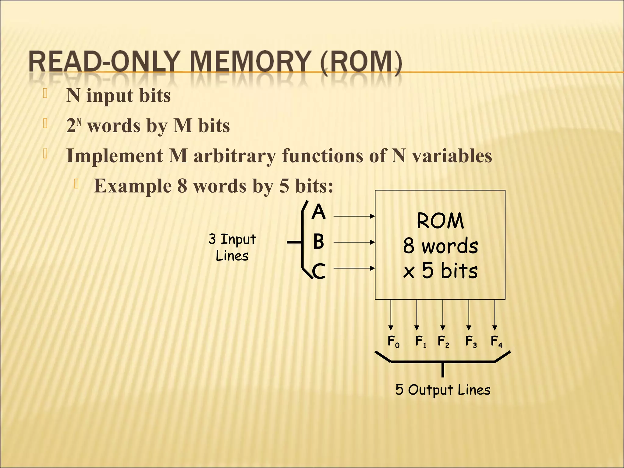
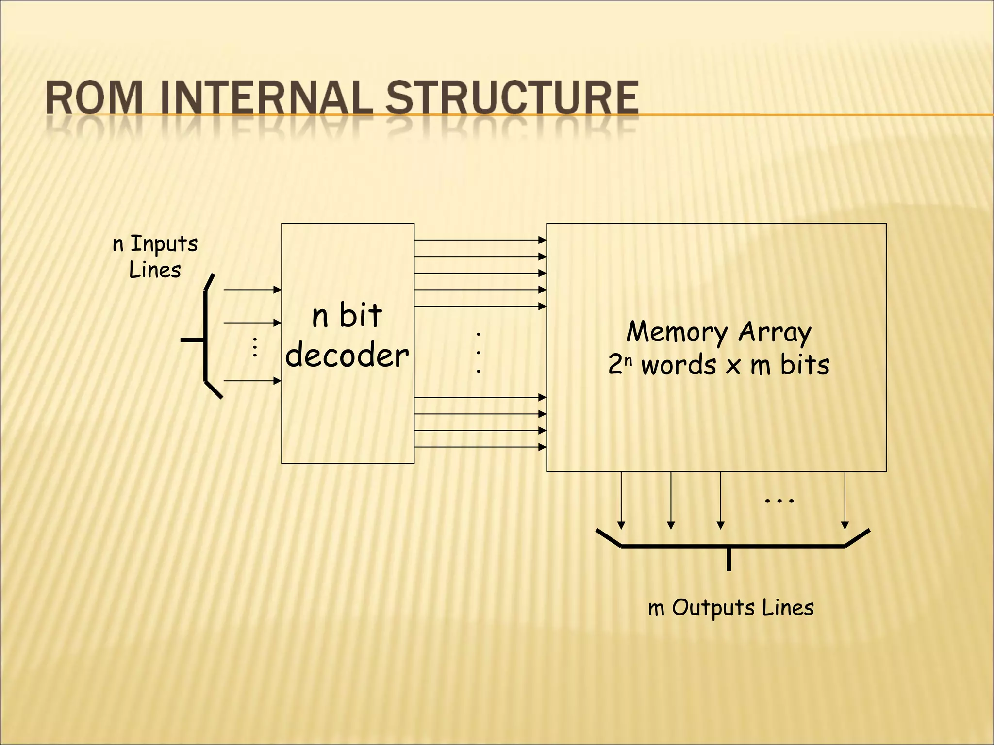
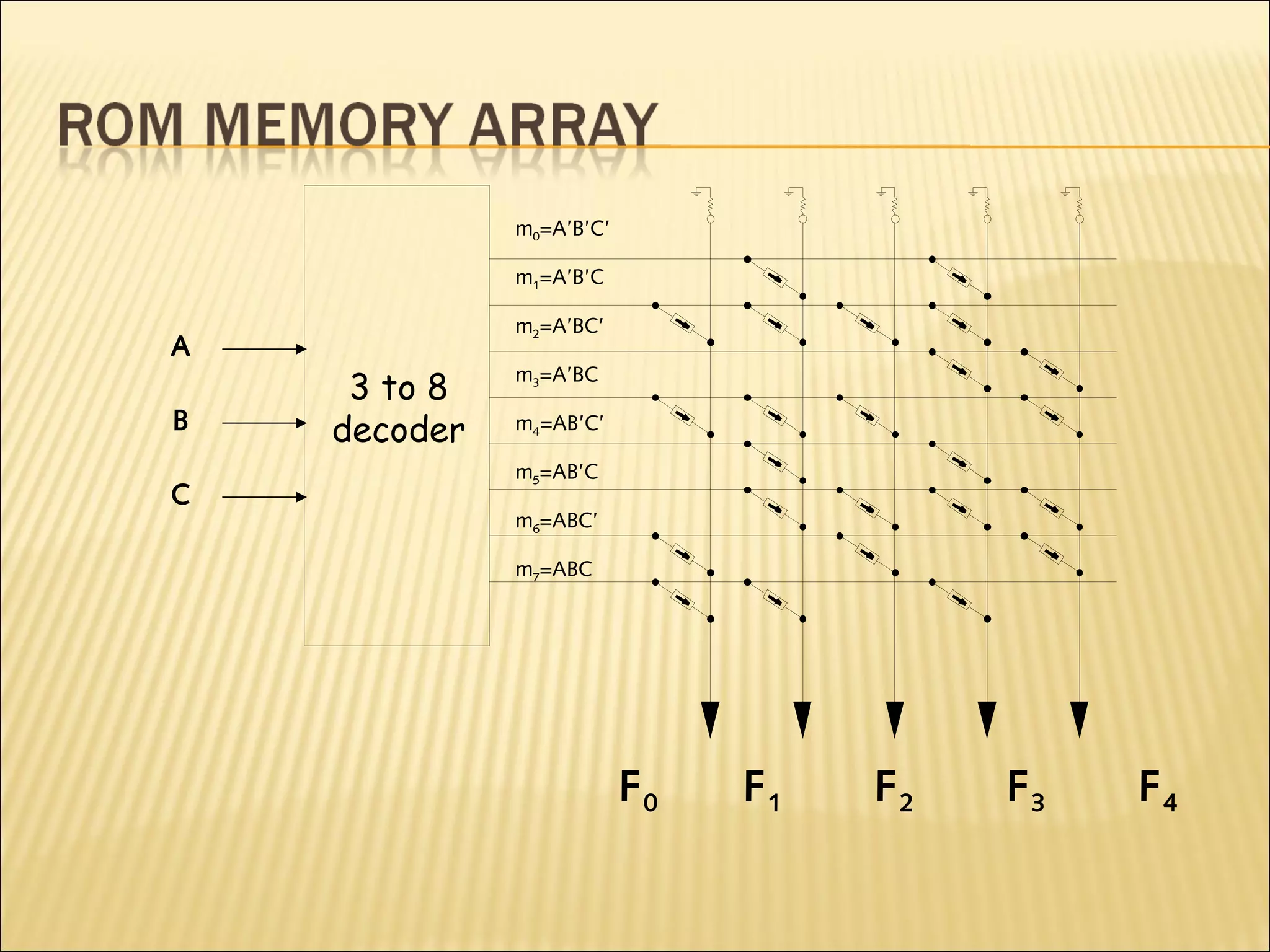
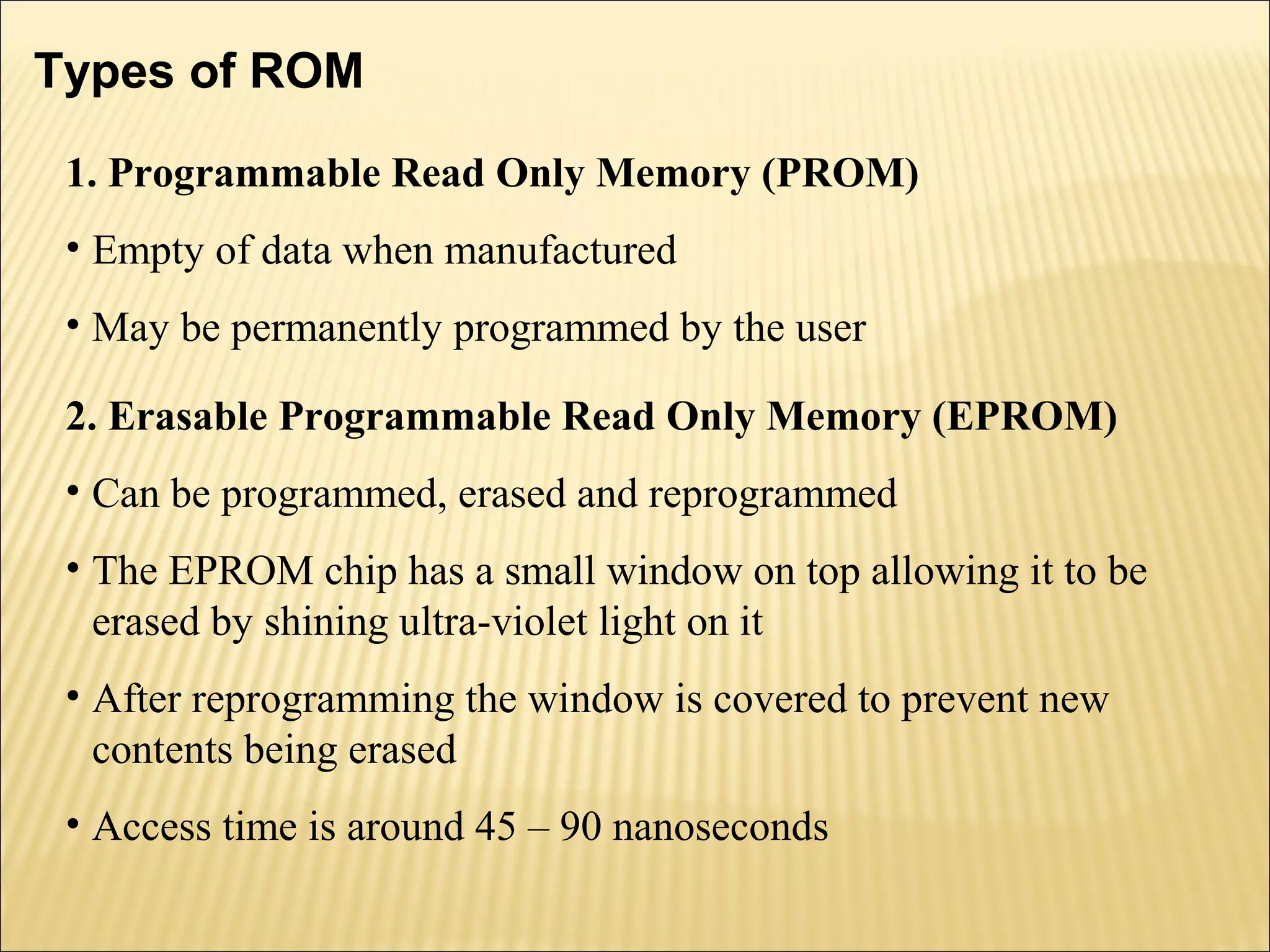
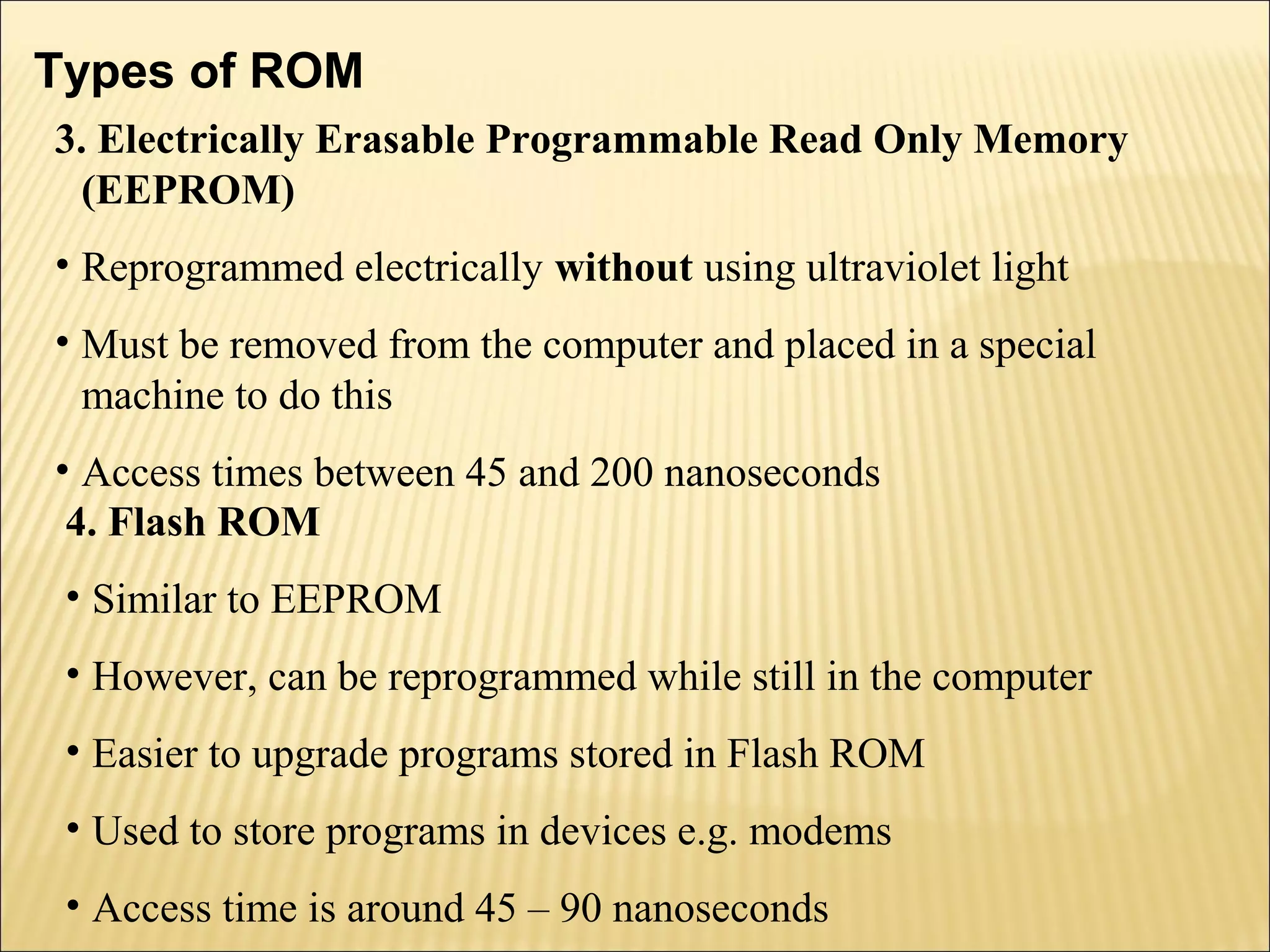
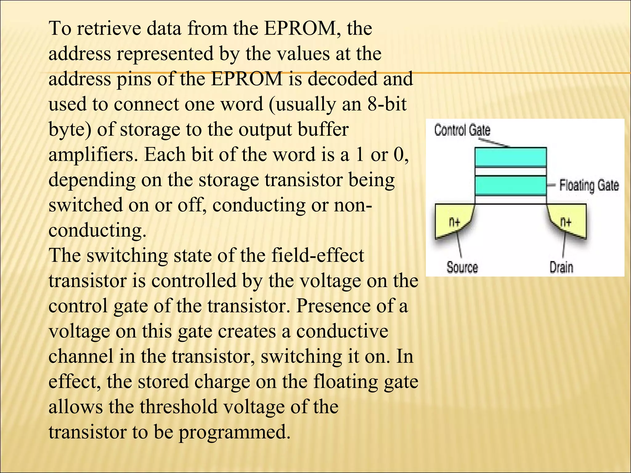
This document provides an overview of read-only memory (ROM) and its variations. It discusses that ROM is a type of memory that retains data permanently, even when power is removed. The document describes the basic components and functioning of ROM, including its input lines, output lines, and decoded minterms. It then explains different types of ROM such as PROM, EPROM, EEPROM, and flash memory, focusing on their ability to be programmed and erased. The document provides details on how each type stores and retrieves data, and their typical access times.
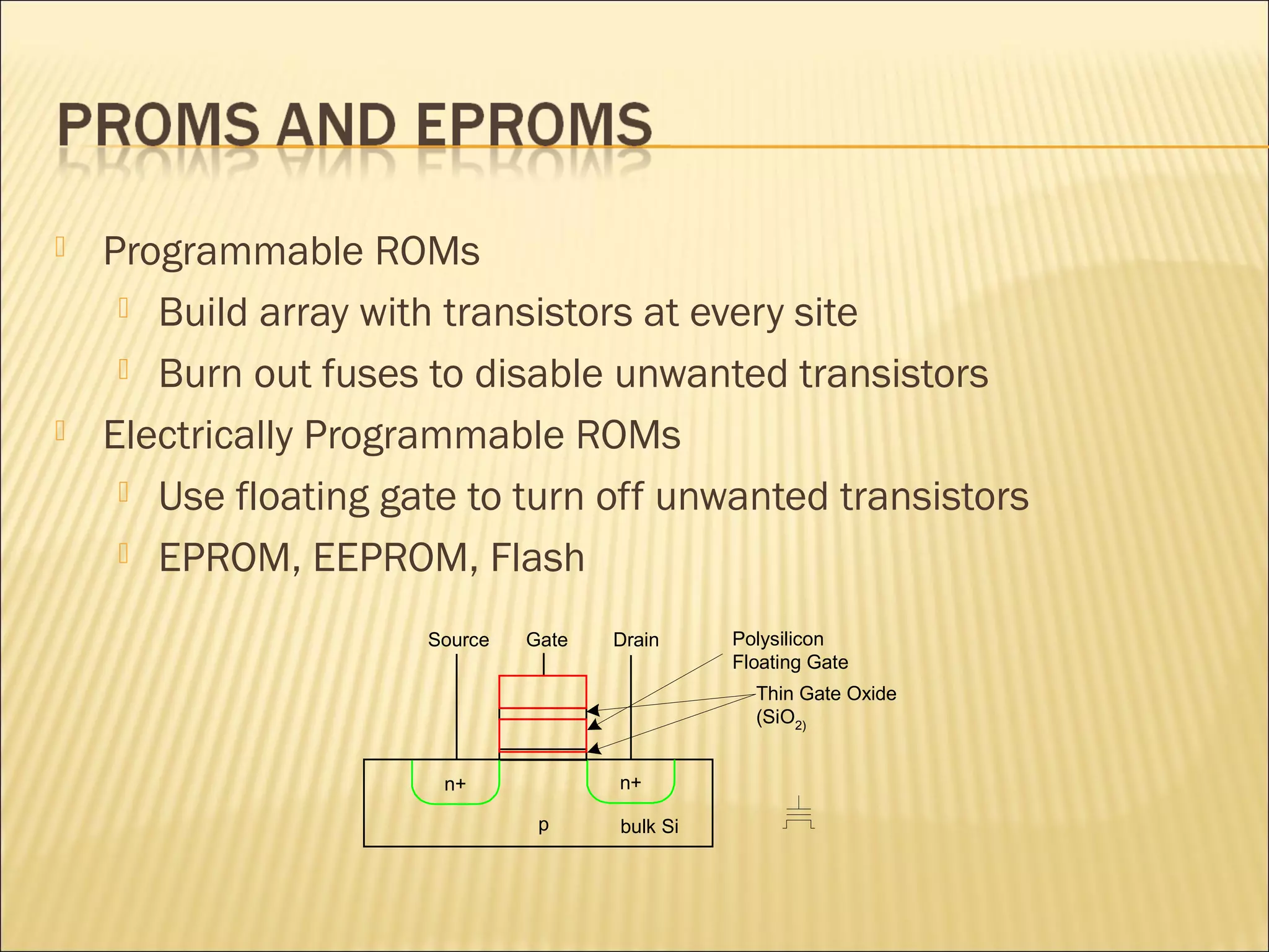
![Storing data in the memory requires selecting a given address and
applying a higher voltage to the transistors. This creates an
avalanche discharge of electrons, which have enough energy to
pass through the insulating oxide layer and accumulate on the gate
electrode. When the high voltage is removed, the electrons are
trapped on the electrode.[3] Because of the high insulation value of
the silicon oxide surrounding the gate, the stored charge cannot
readily leak away and the data can be retained for decades.](https://image.slidesharecdn.com/rom-140919101223-phpapp01/75/Read-Only-Memory-19-2048.jpg)