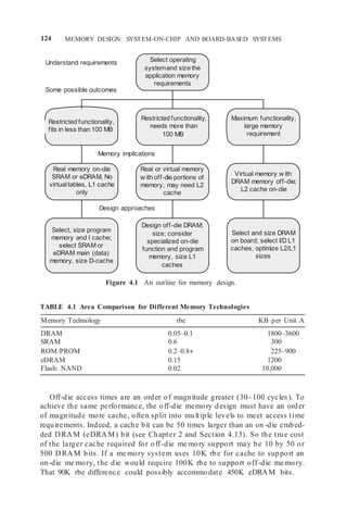
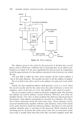
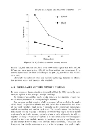
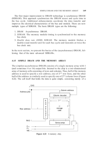
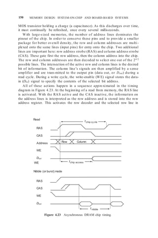
This document discusses memory design considerations for system-on-chip and board-based systems. It begins by explaining that memory system performance largely depends on the memory placement (on-die or off-die), access time, and bandwidth. It then provides an overview of different memory technologies that can be used for on-chip and external memory, such as SRAM, DRAM, flash memory, and discusses their characteristics. The document emphasizes that on-die memory allows faster access times compared to off-die memory, and discusses cache memory design approaches to compensate for longer off-die memory access times.
![126 MEMORY DESIGN: SYSTEM-ON-CHIP AND BOARD-BASED SYSTEMS
TABLE 4.3 Comparison of Flash Memories
Technology NOR NAND
Bit density (KB/A)
Typical capacity
1000
64 MB
10,000
16 GB (dice can be
stacked by 4 or more)
Access time 20–70 ns 10 μs
Transfer rate
(MB per sec.)
150 300
Write time(μs) 300 200
Addressability Word or block Block
Application Program storage and
limited data store
Disk replacement
less than a million. Since degradation with use can be a proble m, error detec-
tion and correction are frequently implemented.
While the density is excellent for semiconductor devices, the write cycle
limitation generally restricts the usage to storing infrequently modified data,
such as programs and large files.
There are two types of flash implementations: NOR and NAND. The NOR
implementation is more flexible, but the NAND provides a significantly better
bit density. Hybrid NOR/NAND imple mentations are also possible with the
NOR array acting as a buffer to the larger NAND array. Table 4.3 provides a
comparison of these implementations.
Flash me mory cards come in various package formats; larger sizes are
usually older (see Table 4.2). Small flash dice can be “stacked” with an SOC
chip to present a single syste m/me mory package. A flash die can also be
stacked to create large (64–256 GB) single memory packages.
In current technology, flash usually is found in off-die imple mentations.
However, there are a number of flash variants that are specifically designed
to be compatible with ordinary SOC technology. SONOS [201] is a nonvolatile
exa mple, and Z-RAM [91] is a DRAM replace ment exa mple. Neither see ms
to suffer from rewrite cycle limitations. Z-RAM seems otherwise compatible
with DRAM speeds while offering improved density. SONOS offers density
but with slower access time than eDRAM.
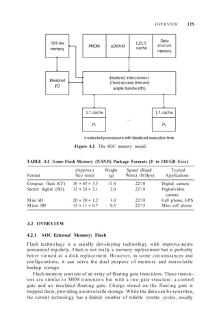
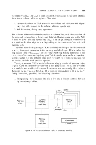
4.2.2 SOC Internal Memory: Placement
The most important and obvious factor in me mory syste m design is the place-
ment of the main me mory: on-die (the same die as the processor) or off-die
(on its own die or on a module with multiple dice). As pointed out in Chapter
1,this factor distinguishes conventional workstation processors and application-
oriented board designs from SOC designs.
The design of the me mory syste m is limited by two basic para meters that
determine memory systems performance. The first is the access time. This is the](https://image.slidesharecdn.com/unit3-220410184730/85/UNIT-3-docx-4-320.jpg)
![BASIC NOTIONS 129
Eliminating the cache control hardware offers additional area for larger
scratchpad size, again improving performance.
SOC imple ments scratchpads usually for data and not for instructions, as
simple caches work well for instructions. Furthermore, it is not worth the
programming effort to directly manage instruction transfers.
The rest of this section treats the theory and experience of cache me mory.
Because there has been so much written about cache, it is easy to forget the
simpler and older scratchpad approach, but with SOC, sometimes the simple
approach is best.
Caches work on the basis of the locality of program behavior [113]. There
are three principles involved:
1. Spatial Locality. Given an access to a particular location in me mory,
there is a high probability that other accesses will be made to either that
or neighboring locations within the lifetime of the program.
2. Temporal Locality. Given a sequence of references to n locations, there
will be references into the same locations with high probability.
3. Sequentiality. Given that a reference has been made to location s, it is
likely that within the next few references, there will be a reference to the
location of s + 1. This is a special case of spatial locality.
The cache designer must deal with the processor’s accessing requirements on
the one hand, and the me mory system’s require ments on the other. Effective
cache designs balance these within cost constraints.
4.4 BASIC NOTIONS
Processor references contained in the cache are called cache hits. References
not found in the cache are called cache misses. On a cache miss, the cache
fetches the missing data from memory and places it in the cache. Usually, the
cache fetches an associated region of memory called the line. The line consists
of one or more physical words accessed fro m a higher-level cache or main
memory. The physical word is the basic unit of access to the memory.
The processor–cache interface has a number of para meters. Those that
directly affect processor performance (Figure 4.4) include the following:
1. Physical word—unit of transfer between processor and cache.
Typical physical word sizes:
2–4 bytes—minimum, used in small core-type processors
8 bytes and larger—multiple instruction issue processors (superscalar)
2. Block size (sometimes called line)—usually the basic unit of transfer
between cache and memory. It consists of n physical words transferred
from the main memory via the bus.](https://image.slidesharecdn.com/unit3-220410184730/85/UNIT-3-docx-7-320.jpg)
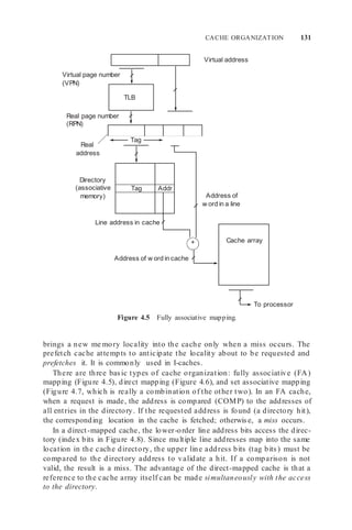
![130 MEMORY DESIGN: SYSTEM-ON-CHIP AND BOARD-BASED SYSTEMS
IS CACHE A PART OF THE PROCESSOR?
For many IP designs, the first-level cache is integrated into the processor
design, so what and why do we need to know cache details? The most
obvious answer is that an SOC consists of multiple processors that must
share memory, usually through a second-level cache. Moreover, the
details of the first-level cache may be essential in achieving memory
consistency and proper program operation. So for our purpose, the cache
is a separate, important piece of the SOC. We design the SOC memory
hierarchy, not an isolated cache.
Figure 4.4 Parameters affecting processor performance.
3. Access time for a cache hit—this is a property of the cache size and
organization.
4. Access time for a cache miss—property of the memory and bus.
5. Time to co mpute a real address given a virtual address (not -in-transla-
tion lookaside buffer [TLB] time) —property of the address translation
facility.
6. Number of processor requests per cycle.
Cache performance is measured by the miss rate or the probability that a
reference made to the cache is not found. The miss rate times the miss time is
the delay penalty due to the cache miss. In simple processors, the processor
stalls on a cache miss.
4.5 CACHE ORGANIZATION
A cache uses either a fetch-on-demand or a prefetch strategy. The former
organization is widely used with simple processors. A demand fetch cache
Addresses
Bus
Cache
Cache size and
miss rate
Physical
word
size
Memory
Access time for
cache miss
To processor
TLB
Not-in-TLB
rate and penalty
Line
size](https://image.slidesharecdn.com/unit3-220410184730/85/UNIT-3-docx-8-320.jpg)
![134 MEMORY DESIGN: SYSTEM-ON-CHIP AND BOARD-BASED SYSTEMS
1.0
Unified cache
0.1
0.01
0.001
10 100 1000 10,000 100,000 1,000,000
Cache size (bytes)
Figure 4.9 A design target miss rate per reference to memory (fully associative,
demand fetch, fetch [allocate] on write, copy-back with LRU replacement) [223, 224].
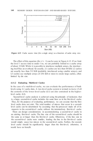
memory and program size were fixed and small. Such data show low miss rate
for relatively small size caches. Thus, there is a tendency for the measured miss
rate of a particular cache size to increase over time. This is simply the result
of measurements made on programs of increasing size. Some time ago, Smith
[224] developed a series of design target miss rates (DTMRs) that represent
an estimate of what a designer could expect fro m an integrated (instruction
and data) cache. These data are presented in Figure 4.9 and give an idea of
typical miss rates as a function of cache and line sizes.
For cache sizes largerthan 1 MB, a general rule is that doubling the size halves
the miss rate. The general rule is less valid in transaction-based programs.
4.7 WRITE POLICIES
How is me mory updated on a write? One could write to both cache and
memory (write-through or WT), or write only to the cache (copy -back or CB—
sometimes called write-back), updating me mory when the line is replaced.
These two strategies are the basic cache write policies (Figure 4.10).
The write-through cache (Figure 4.10a) stores into both cache and main
memory on each CPU store.
Advantage: This retains a consistent (up-to-date) image of program activity
in memory.
Disadvantage: Memory bandwidth may be high—dominated by write traffic.
In the copy-back cache (Figure 4.10b), the new data are written to memory
when the line is replaced. This requires keeping track of modified (or “dirty”)
lines, but results in reduced memory traffic for writes:
Line size (bytes)
4
8
16
32
64
128
Design
target
miss
rate](https://image.slidesharecdn.com/unit3-220410184730/85/UNIT-3-docx-12-320.jpg)
![ST RATEGIES FOR LINE REPLACEMENT AT MISS TIME 135
Cache
If not in cache, update memory
Memory
(a) Write-through
Write
(b) Write-back(copy-back)
Memory
Write
Figure 4.10 Write policies: (a) write-through cache (no allocate on write) and (b) copy-
back cache (allocate on write).
1. Dirty bit is set if a write occurs anywhere in line.
2. Fro m various traces [223], the probability that a line to be replaced is
dirty is 47% on average (ranging from 22% to 80%).
3. Rule of thu mb: Half of the data lines replaced are dirty. So, for a data
cache, assu me 50% are dirty lines, and for an integrated cache, assume
30% are dirty lines.
Most larger caches use copy-back; write-through is usually restricted to either
small caches or special-purpose caches that provide an up -to-date image of
memory. Finally, what should we do when a write (or store) instruction misses
in the cache? We can fetch that line from me mory (write allocate or WA) or
just write into memory (no write allocate or NWA). Most write-through caches
do not allocate on writes (WTNWA) and most copy back caches do allocate
(CBWA).
4.8 STRATEGIES FOR LINE REPLACEMENT AT MISS TIME
What happens on a cache miss? If the reference address is not found in the
directory, a cache miss occurs. Two actions must pro mptly be taken: (1) The
missed line must be fetched from the main memory, and (2) one of the current
Cache Write line on
replacement](https://image.slidesharecdn.com/unit3-220410184730/85/UNIT-3-docx-13-320.jpg)
![ST RATEGIES FOR LINE REPLACEMENT AT MISS TIME 137
effects
DTMR
(memory references)
100
1000
10,000
20,000
100,000
While LRU performs better than either FIFO or RAND, the use of the
simpler RAND or FIFO only amplifies the LRU miss rate (DTMR) by about
1.10 (i.e., 10%) [223].
4.8.3 Cache Environment: Effects of System, Transactions,
and Multiprogramming
Most available cache data are based upon trace studies of user applications.
Actual applications are run in the context of the system. The operating system
tends to slightly increase (20% or so) the miss rate e xperienced by a user
program [7].
Multiprogramming environments create special demands on a cache. In
such environ ments, the cache miss rates may not be affected by increasing
cache size. There are two environments:
1. A Multiprogrammed Environment. The system, together with several
progra ms, is resident in me mory. Control is passed fro m program to
progra m after a nu mber of instructions, Q, have been executed, and
eventually returns to the first program. This kind of environment results
in what is called a warm cache. When a process returns for continuing
execution, it finds some, but not all, of its most recently used lines in the
cache, increasing the expected miss rate (Figure 4.11 illustrates the
effect).
2. Transaction Processing. While the system is resident in memory together
with a number of support programs, short applications (transactions) run
1.0
Multiprogramming level = 2
Line size = 16 bytes
0.1
0.01
0.001
10 100 1000 10,000 100,000 1,000,000
Cache size
Figure 4.11 Warm cache: cache miss rates for a multiprogrammed environment
switching processes after Q instructions.
Miss
rate](https://image.slidesharecdn.com/unit3-220410184730/85/UNIT-3-docx-15-320.jpg)
![MULTILEVEL CACHES 139
TABLE 4.5 Common Types of Cache
Type Where It Is Usually Used
Integrated (or unified) The basic cache that accommodates all references (I
and D). This is commonly used as the second- and
higher-level cache.
Split caches I and D Provides additional cache access bandwidth with some
increase in the miss rate (MR). Commonly used as a
first-level processor cache.
Sectored cache Improves area effectiveness (MR for given area) for
on-chip cache.
Multilevel cache The first level has fast access; the second level is usually
much larger than the first to reduce time delay in a
first-level miss.
Write assembly cache Specialized, reduces write traffic, usually used with a WT
on-chip first-level cache.
code and user code or even special input/output (I/O) caches have been con -
sidered. The most popular configuration of partitioned caches is the use of
separate caches for instructions and data.
Separate instruction and data caches provide significantly increased cache
bandwidth, doubling the access capability of the cache ense mble. I - and D-
caches come at some expense, however; a unified cache with the same size as
the sum of a data and instruction cache has a lower miss rate. In the unified
cache, the ratio of instruction to data working set elements changes during the
execution of the program and is adapted to by the replacement strategy.
Split caches have implementation advantages. Since the caches need not be
split equally, a 75–25% or other split may prove more effective. Also, the I-
cache is simpler as it is not required to handle stores.
4.11 MULTILEVEL CACHES
4.11.1 Limits on Cache Array Size
The cache consists of a static RAM (SRAM) array of storage cells. As the
array increases in size, so does the length of the wires required to access its
most remote cell. This translates into the cache access delay, which is a function
of the cache size, organization, and the process technology (feature size, f).
McFarland [166] has modeled the delay and found that an appro ximation can
be represented as
Access time ns 0.35 3.8 f 0.006 0.025 f C 1 0.31 1 A,
where f is the feature size in microns, C is the cache array capacity in kilobyte,
and A is the degree of associativity (where direct map = 1).](https://image.slidesharecdn.com/unit3-220410184730/85/UNIT-3-docx-17-320.jpg)
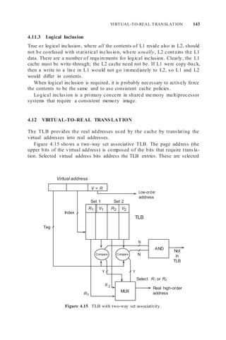
![MULTILEVEL CACHES 141
Memory
References
Figure 4.14 A two-level cache.
In a two-level system, as shown in Figure 4.14, with first-level cache, L1, and
second-level cache, L2, we define the following miss rates [202]:
1. A local miss rate is simply the number of misses experienced by the cache
divided by the number of references to it. This is the usual understanding
of miss rate.
2. The global miss rate is the nu mber of L2 misses divided by the number
of references made by the processor. This is our primary measure of the
L2 cache.
3. The solo miss rate is the miss rate the L2 cache would have if it were the
only cache in the system. This is the miss rate defined by the principle of
inclusion. If L2 contains all of L1, then we can find the number of L2
misses and the processor reference rate, ignoring the presence of the L1
cache. The principle of inclusion specifies that the global miss rate is the
same as the solo miss rate, allowing us to use the solo miss rate to evalu -
ate a design.
The preceding data (read misses only) illustrate some salient points in multi-
level cache analysis and design:
1. So long as the L1 cache is the same as or larger than the L2 cache, analy -
sis by the principle of inclusion provides a good estimate of the behavior
of the L2 cache.
2. When the L2 cache is significantly larger than the L1 cache, it can be
considered independent of the L1 para meters. Its miss rate corresponds
to a solo miss rate.
Processor
L1
cache
L2
cache](https://image.slidesharecdn.com/unit3-220410184730/85/UNIT-3-docx-19-320.jpg)
![142 MEMORY DESIGN: SYSTEM-ON-CHIP AND BOARD-BASED SYSTEMS
EXAMPLE 4.1
Miss penalties:
L2 more than four times the L1 size
Miss in L1, hit in L2: 2 cycles
Miss in L1, miss in L2: 15 cycles
Suppose we have a two-level cache with miss rates of 4% (L1) and 1% (L2).
Suppose the miss in L1 and the hit in L2 penalty is 2 cycles, and the miss
penalty in both caches is 15 cycles (13 cycles more than a hit in L2). If a pro-
cessor makes one reference per instruction, we can compute the excess cycles
per instruction (CPIs) due to cache misses as follows:
Excess CPI due to L1 misses
1.0 refr inst 0.04 misses refr 2 cycles miss
0.08 CPI
Excess CPI due to L2 misses
1.0 refr inst 0.01 misses refr 13 cycles miss
0.13 CPI.
Note: the L2 miss penalty is 13 cycles, not 15 cycles, since the 1% L2 misses
have already been “charged” 2 cycles in the excess L1 CPI:
Total effect excess L1 CPI excess L2 CPI
0.08 0.13
0.21 CPI.
The cache configurations for some recent SOCs are shown in Table 4.6.
TABLE 4.6 SOC Cache Organization
SOC L1 Cache L2 Cache
NetSilicon NS9775 [185] 8-KB I-cache, 4-KB D-cache —
NXP LH7A404 [186] 8-KB I-cache, 8-KB D-cache —
Freescale e600 [101] 32-KB I-cache, 32-KB D-cache 1 MB with ECC
Freescale PowerQUICC
III [102]
32-KB I-cache, 32-KB D-cache 256 KB with ECC
ARM1136J(F)-S [24] 64-KB I-cache, 64-KB D-cache Max 512 KB
L1
L2](https://image.slidesharecdn.com/unit3-220410184730/85/UNIT-3-docx-20-320.jpg)
![SOC (ON-DIE) MEMORY SYSTEMS 145
TABLE 4.7 SOC TLB Organization
SOC Organization Number of Entries
Freescale e600 [101] Separate I-TLB, D-TLB 128-entry, two-way set
associative, LRU
NXP LH7A404 [186] Separate I-TLB, D-TLB 64-entry each
NetSilicon NS9775
(ARM926EJ-S) [185]
Mixed 32-entry two-way set
associative
Excess not-in-TLB translations can generally be controlled through the use of
a well-designed TLB. The size and organization of the TLB depends on per-
formance targets.
Typically, separate instruction and data TLBs are used. Both TLBs might
use 128-entry, two-way set associative, and might use LRU replacement algo-
rithm. The TLB conflagrations of some recent SOCs are shown in Table 4.7.
4.13 SOC (ON-DIE) MEMORY SYSTEMS
On-die me mory design is a special case of the general me mory syste m design
problem, considered in the next section. The designer has much greater flex-
ibility in the selection of the me mory itself and the overall cache -me mory
organization. Since the application is known, the general size of both the
progra m and data store can be estimated. Frequently, part of the progra m store
is designed as a fixed ROM. The remainder of memory is realized with either
SRAM or DRAM. While the SRAM is realized in the same process technol-
ogy as the processor, usually DRAM is not. An SRAM bit consists of a six-
transistor cell, while the DRAM uses only one transistor plus a deep trench
capacitor. The DRAM cell is designed for density; it uses few wiring layers.
DRAM design targets low refresh rates and hence low leakage currents. A
DRAM cell uses a nonminimu m length transistor with a higher threshold
voltage, (VT), to provide a lower-leakage current. This leads to lower gate
overdrive and slower switching. For a stand -alone die, the result is that the
SRAM is 10–20 times faster and 10 or more times less dense than DRAM.
eDRAM [33, 125] has been introduced as a compromise for use as an on-die
me mory. Since there are additional process steps in realizing an SOC with
eDRAM, the macro to generate the eDRAM is fabrication specific and is
regarded as a hard (or at least firm) IP. The eDRAM has an overhead (Figure
4.17) resulting in less density than DRAM. Process complexity for the eDRAM
can include generating three additional mask layers resulting in 20% addi-
tional cost than that for the DRAM.
An SOC, using the eDRAM approach, integrates high-speed, high-leakage
logic transistors with lower-speed, lower-leakage me mory transistors on the
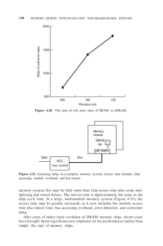
same die. The advantage for eDRAM lies in its density as shown in Figure
4.18. Therefore, one key factor for selecting eDRAM over SRAM is the size
of the memory required.](https://image.slidesharecdn.com/unit3-220410184730/85/UNIT-3-docx-23-320.jpg)
![152 MEMORY DESIGN: SYSTEM-ON-CHIP AND BOARD-BASED SYSTEMS
[00] [01] [10] [11]
2. the creation of the correct RAS and CAS signal lines at the appropriate
time, and
3. providing a timely refresh of the memory system.
Since the dynamic me mory controller output drives all p bits, and hence p
chips, of the physical word, the controller output may also require buffering.
As the me mory read operation is completed, the data-out signals are directed
at bus drivers, which then interface to the memory bus, which is the interface
for all of the memory modules.
Two features found on DRAM chips affect the design of the me mory
system. These “burst” mode-type features are called
1. nibble mode and
2. page mode.
Both of these are techniques for improving the transfer rate of me mory
words. In nibble mode, a single address (row and colu mn) is presented to
the me mory chip and the CAS line is toggled repeatedly. Internally, the chip
interprets this CAS toggling as a mod 2w
progression of low-order column
addresses. Thus, sequential words can be accessed at a higher rate from the
me mory chip. For exa mple, for w = 2, we could access four consecutive low-
order bit addresses, for example:
and then return to the original bit address.
In page mode, a single row is selected and nonsequential column addresses
may be entered at a high rate by repeatedly activating the CAS line (similar
to nibble mode, Figure 4.23). Usually, this is used to fill a cache line.
While terminology varies, the nibble mode usually refers to the access of
(up to) four consecutive words (a nibble) starting on a quad word address
boundary. Table 4.8 illustrates some SOC memory size, position and type. The
newer DDR SDRAM and follow ons are discussed in the next section.
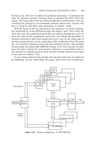
4.15.1 SDRAM and DDR SDRAM
The first major improvement to the DRAM technology is the SDRAM. This
approach, as mentioned before, synchronizes the DRAM access and cycle to
TABLE 4.8 SOC Memory Designs
SOC Memory Type Memory Size Memory Position
Intel PXA27x [132] SRAM 256 KB On-die
Philips Nexperia
PNX1700 [199]
DDR SDRAM 256 MB Off-die
Intel IOP333 [131] DDR SDRAM 2 GB Off-die](https://image.slidesharecdn.com/unit3-220410184730/85/UNIT-3-docx-30-320.jpg)
![154 MEMORY DESIGN: SYSTEM-ON-CHIP AND BOARD-BASED SYSTEMS
Row and Bank
Address Active Column Address D1 D2 D3 D4
One Cycle One Cycle
Figure 4.26 A line fetch in DDR SDRAM.
then the row activation time must be added to the access time. Another
improvement introduced in SDRAMs is the use of multiple DRAM arrays,
usually either four or eight. Depending on the chip imple mentation, these
multiple arrays can be independently accessed or sequentially accessed, as
programmed by the user. In the former case, each array can have an indepen-
dently activated row providing an interleaved access to multiple colu mn
addresses. If the arrays are sequentially accessed, then the corresponding rows
in each array are activated and longer bursts of consecutive data can be sup-
ported. This is particularly valuable for graphics applications.
The improved timing parameters of the modern me mory chip results fro m
careful attention to the electrical characteristic of the bus and the chip. In
addition to the use of differential signaling (initially for data, now for all
signals), the bus is designed to be a terminated strip transmission line. With
the DDR3 (closely related to graphics double data rate [GDDR3]), the ter-
mination is on-die (rather than simply at the end of the bus), and special cali-
bration techniques are used to ensure accurate termination.
The DDR chips that support interleaved row accesses with independent
arrays must carry out a 2n data fetch from the array to support the DDR. So,
a chip with four data out (n = 4) lines must have arrays that fetch 8 bits. The
DDR2 arrays typically fetch 4n, so with n = 4, the array would fetch 16 bits.
This enables higher data transmission rates as the array is accessed only once
for every four-bus half-cycles.
Some typical parameters are shown in Tables 4.9 and 4.10. While represen-
tatives of all of these DRAMs are in production at the time of writing, the
asynchronous DRAM and the SDRAM are legacy parts and are generally not
used for new development. The DDR3 part was introduced for graphic appli-
cation configurations. For most cases, the parameters are typical and for
common configurations. For example, the asynchronous DRAM is available
with 1, 4, and 16 output pins. The DDR SDRAMs are available with 4, 8, and
16 output pins. Many other arrangements are possible.
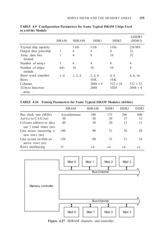
Multiple (up to four) DDR2 SDRAMs can be configured to share a common
bus (Figure 4.27). In this case, when a chip is “active” (i.e., it has an active row),](https://image.slidesharecdn.com/unit3-220410184730/85/UNIT-3-docx-32-320.jpg)
![158 MEMORY DESIGN: SYSTEM-ON-CHIP AND BOARD-BASED SYSTEMS
n processors
making one request
each Tc
One processor
making n requests
each Tc
Modeling assumption: Asymptotically, these are equivalent.
Figure 4.28 Finding simple processor equivalence.
an equivalent multiple processor, the designer must determine the number of
requests to the memory module per module service time, Ts = Tc.
A simple processor makes a single request and waits for a response fro m
me mory. A pipelined processor makes multiple requests for various buffers
before waiting for a memory response. There is an approximate equivalence
between n simple processors, each requesting once every Ts, and one pipelined
processor making n requests every Ts (Figure 4.28).
In the following discussion, we use two symbols to represent the bandwidth
available from the memory system (the achieved bandwidth):
1. B. The number of requests that are serviced each Ts . Occasionally, we
also specify the arguments that B takes on, for exa mple, B (m, n) or B
(m).
2. Bw. The number of requests that are serviced per second: Bw = B/Ts.
To translate this into cache-based systems, the service time, Ts, is the time that
the memory system is busy managing a cache miss. The number of memory
modules, m, is the maximum number of cache misses that the memory system
can handle at one time, and n is the total number of request per Ts . This is the
total number of expected misses per processor per Ts multiplied by the number
of processors making requests.
4.16.2 The Strecker-Ravi Model
This is a simple yet useful model for estimating contention. The original model
was developed by Strecker [229] and independently by Ravi [204]. It assumes
that there are n simple processor requests made per me mory cycle and there
are m me mory modules. Further, we assume that there is no bus contention.
The Strecker model assumes that the me mory request pattern for the proces -
sors is uniform and the probability of any one request to a particular me mory
module is simply 1/m. The key modeling assumption is that the state of the](https://image.slidesharecdn.com/unit3-220410184730/85/UNIT-3-docx-36-320.jpg)
![MODELS OF SIMPLE PROCESSOR–MEMORY INTERACTION 159
memory system at the beginning of the cycle is not dependent upon any previ-
ous action on the part of the me mory—hence, not dependent upon contention
in the past (i.e., Markovian). Unserved requests are discarded at the end of
the memory cycle.
The following modeling approximations are made:
1. A processor issues a request as soon as its previous request has been
satisfied.
2. The me mory request pattern from each processor is assumed to be uni-
formly distributed; that is, the probability of any one request being made
to a particular memory module is 1/m.
3. The state of the me mory system at the beginning of each me mory
cycle (i.e., which processors are awaiting service at which modules) is
ignored by assuming that all unserviced requests are discarded at the
end of each me mory cycle and that the processors rando mly issue new
requests.
Analysis:
Let the average nu mber of me mory requests serviced per me mory cycle be
represented by B (m, n). This is also equal to the average number of memory
modules busy during each me mory cycle. Looking at events from any given
module’s point of view during each memory cycle, we have
Prob a given processor does not reference the module 1 1 m
Prob no processor references the module Prob the module is idle
11 m
Prob the module is busy 1 1 1 mn
B m, n average number of busy modules m1 1 1 mn
.
The achieved memory bandwidth is less than the theoretical maximum due to
contention. By neglecting congestion in previous cycles, this analysis results in
an optimistic value for the bandwidth. Still, it is a simple estimate that should
be used conservatively.
It has been shown by Bhandarkar [41] that B (m, n) is almost perfectly
symmetrical in m and n. He exploited this fact to develop a more accurate
expression for B (m, n), which is
Bm, n K 111 Kl
,
where K = max (m, n) and l = min (m, n).
We can use this to model a typical processor ensemble.](https://image.slidesharecdn.com/unit3-220410184730/85/UNIT-3-docx-37-320.jpg)


![[G2]fa ce deview_2012](https://cdn.slidesharecdn.com/ss_thumbnails/g2facedeview2012-120919022734-phpapp02-thumbnail.jpg?width=640&height=640&fit=bounds)