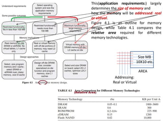
The document discusses memory design for system-on-chip (SOC) devices. It covers several key aspects of SOC memory design:
1. The primary considerations for memory design are the application requirements which determine the size of memory and addressing scheme (real or virtual).
2. Internal memory placement on the same die as the processor allows much faster access times than external off-die memory. On-die memory is limited in size by chip area constraints.
3. Caches and scratchpad memories can be used to improve performance by keeping frequently used data and instructions close to the processor core. Caches rely on locality of reference principles while scratchpads require direct programmer management.


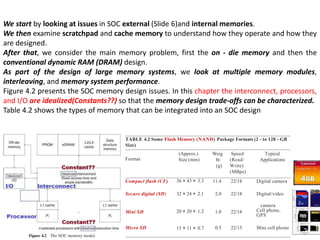
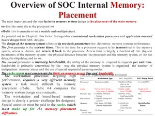

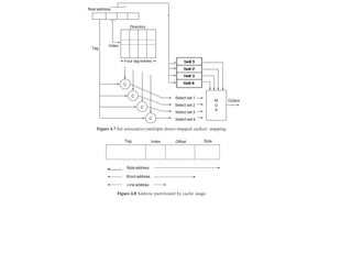
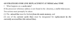
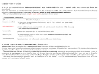
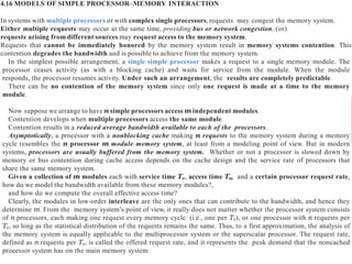
![BASIC NOTIONS
• Processor references contained in the cache are called cache hits.
• Processor references not found in the cache are called cache misses.
• On a cache miss, the cache fetches the missing data from memory and places it in the cache.
• Usually, the cache fetches an associated region of memory called the line. The line consists of one or more physical
words accessed from a higher-level cache or main memory. The physical word is the basic unit of access to the memory.
• The processor–cache interface has a number(6) of parameters. Those that directly affect processor performance (Figure
4.4) include the following 6 parameters :
1. Physical word—unit of transfer between processor and cache. Typical physical word sizes:
• 2–4 bytes—minimum, used in small core-type processors
• 8 bytes and larger—multiple instruction issue processors (superscalar)
2. Block size (sometimes called line)—usually the basic unit of transfer between cache and memory. It consists of n
physical words transferred from the main memory via the bus.
3. Access time for a cache hit—this is a property of the cache size and organization.
4. Access time for a cache miss—property of the memory and bus.
5. Time to compute a real address given a virtual address (not-in-translation look aside buffer [TLB] time)—property of the
address translation facility.
6. Number of processor requests per cycle.
Cache performance is measured by the miss rate or the probability that a reference made to the cache is not found. The miss
rate times the miss time is the delay penalty due to the cache miss. In simple processors, the processor stalls on a cache miss.
IS CACHE A PART OF THE PROCESSOR?
For many IP designs, t h e f i r s t - l e v e l c a c h e i s
i n t e g r a t e d i n t o t h e p r o c e s s o r d e s i g n , so what
and why do we need to know cache details? The most obvious answer
is that an SOC consists of multiple processors that must share
memory, usually through a second-level cache. Moreover, the details
of the first-level cache may be essential in achieving memory
consistency and proper program operation. So for our purpose, the cache
is a separate, important piece of the SOC. We design the SOC memory
hierarchy, not an isolated cache.](https://image.slidesharecdn.com/unit3memorydesignforsoc-240222144045-142bc49b/85/UNIT-3-Memory-Design-for-SOC-ppUNIT-3-Memory-Design-for-SOC-pptx-11-320.jpg)

![0.01
134 MEMORY DESIGN: SYSTEM-ON-CHIP AND BOARD-BASEDSYSTEMS
Unified cache
1.0
Design
target
miss
rate
8
16
32
64
128
0.1
Line size (bytes)
4
0.001
10 100 1000 10,000 100,000 1,000,000
Cache size (bytes)
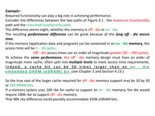
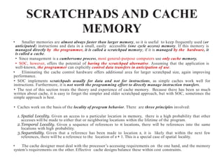
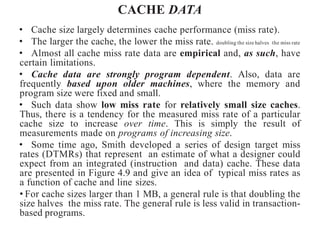
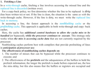
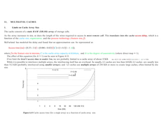
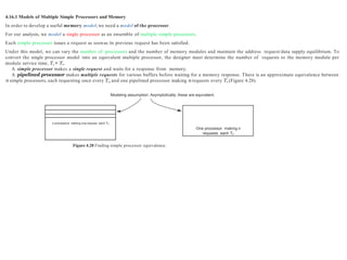
Figure 4.9 A design target miss rate per reference to memory (fully associative,
demand fetch, fetch [allocate] on write, copy-back with LRU replacement) [223, 224].](https://image.slidesharecdn.com/unit3memorydesignforsoc-240222144045-142bc49b/85/UNIT-3-Memory-Design-for-SOC-ppUNIT-3-Memory-Design-for-SOC-pptx-17-320.jpg)
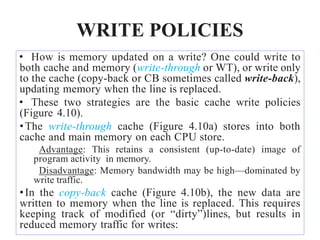
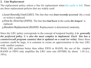
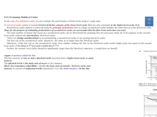
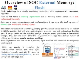
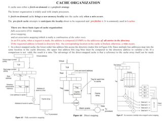
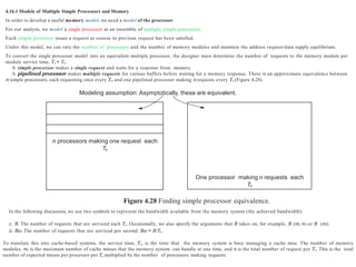
![EXAMPLE 4.1
SOC L1 Cache L2 Cache
NetSilicon NS9775 [185]
NXP LH7A404 [186]
Freescale e600 [101] Freescale
PowerQUICC
III [102]
ARM1136J(F)-S [24]
8-KB I-cache, 4-KB D-cache 8-KB I-cache, 8-KB D-
cache
32-KB I-cache, 32-KB D-cache 32-KB I-cache, 32-KB
D-cache
—
—
1 MB with ECC 256 KBwith
ECC
64-KB I-cache, 64-KB D-cache Max 512KB
L1
L2
L2 more than four times the L1 size
Miss penalties:
Miss in L1, hit in L2:
Miss in L1, miss in L2:
2 cycles
15 cycles
Suppose we have a two-level cache with miss rates of 4% (L1) and 1% (L2). Suppose the miss in L1 and the hit in L2 penalty is 2
cycles, and the miss penalty in both caches is 15 cycles (13 cycles more than a hit in L2). If a processor makes one reference per
instruction, we can compute the excess Cycles Per Instruction (CPIs) due to cache misses as follows:
Excess CPI due to L1 misses
1.0 refr/ inst 0.04 misses /refr 2 cycles/ miss
0.08 CPI
Excess CPI due to L2 misses
1.0 refr/ inst 0.01 misses/ refr 13 cycles/ miss
0.13 CPI.
Note: the L2 miss penalty is 13 cycles, not 15 cycles, since the 1% L2 misses have already been “charged” 2 cycles in the excess L1 CPI:
Total effect excess L1 CPI excess L2 CPI
0.08 0.13
0.21CPI.
The cache configurations for some recent SOCs are shown in Table 4.6.
TABLE 4.6 SOC Cache Organization](https://image.slidesharecdn.com/unit3memorydesignforsoc-240222144045-142bc49b/85/UNIT-3-Memory-Design-for-SOC-ppUNIT-3-Memory-Design-for-SOC-pptx-28-320.jpg)
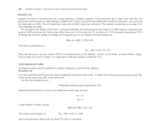
![4.16.2 The Strecker-Ravi Model
This is a simple yet useful model for estimating contention. The original model was developed by Strecker and independently by Ravi.
It assumes that there are n simple processor requests made per memory cycle and
there are mmemory modules.
Further, we assume that there is no bus contention.
The Strecker model assumes that the memory request pattern for the processors is uniform and the probability of any one request to a particular
memory module is simply 1/m.
The key modeling assumption is that the state of the memory system at the beginning of the cycle is not dependent upon any previous action on the part
of the memory—hence, not dependent upon contention in the past (i.e., Markovian). Unserved requests are discarded at the end of the memory cycle.
The following modeling approximations are made:
1. A processor issues a request as soon as its previous request has been satisfied.
2. The memory request pattern from each processor is assumed to be uni- formly distributed; that is, the probability of any one request being made
to a particular memory module is 1/m.
3. The state of the memory system at the beginning of each memory cycle (i.e., which processors are awaiting service at which modules) is ignored
by assuming that all unserviced requests are discarded at the end of each memory cycle and that the processors randomly issue new requests.
Analysis:
Let the average number of memory requests serviced per memory cycle be represented by B (m, n). This is also equal to the average number of
memory modules busy during each memory cycle. Looking at events from any given module’s point of view during each memory cycle, we have
Prob a given processor does not reference the module 1 1/m
Prob no processor references the module Prob the module is idle 1 1/m
Prob the module is busy 1 1 1/mn
B m, n average number of busy modules m1 1 1/mn
.
The achieved memory bandwidth is less than the theoretical maximum due to contention. By neglecting congestion in previous cycles, this analysis
results in an optimistic value for the bandwidth. Still, it is a simple estimate that should be used conservatively.
It has been shown by Bhandarkar [41] that B (m, n) is almost perfectly symmetrical in m and n. He exploited this fact to develop a more accurate
expression for B (m, n), which is
Bm, n K [11 1/K l
] where K = max (m, n) and l = min (me, n).
We can use this to model a typical processor ensemble.](https://image.slidesharecdn.com/unit3memorydesignforsoc-240222144045-142bc49b/85/UNIT-3-Memory-Design-for-SOC-ppUNIT-3-Memory-Design-for-SOC-pptx-32-320.jpg)


![[G2]fa ce deview_2012](https://cdn.slidesharecdn.com/ss_thumbnails/g2facedeview2012-120919022734-phpapp02-thumbnail.jpg?width=640&height=640&fit=bounds)