Download as PDF, PPTX


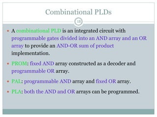
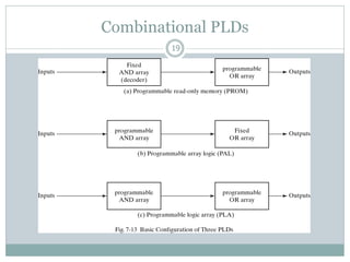


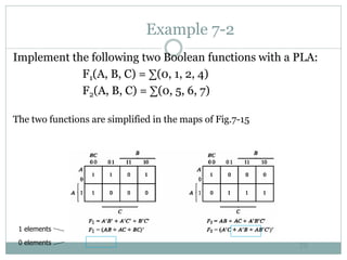
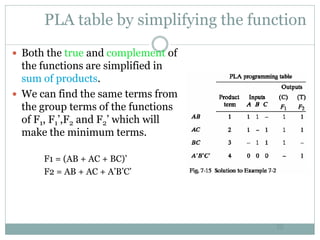
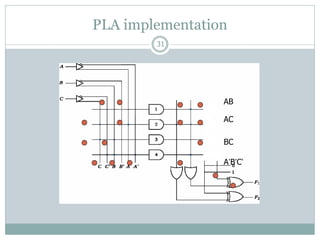

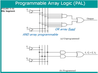
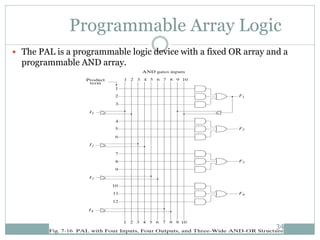


This document provides an introduction to programmable logic devices including read-only memory (ROM) and programmable logic arrays (PLA). It discusses the basic components and operations of random-access memory (RAM) and ROM. It then describes how PLA and programmable array logic (PAL) work, using AND-OR logic to implement combinational logic functions. Examples are provided to demonstrate how to design circuits using these programmable logic devices and simplify Boolean functions for efficient implementation.