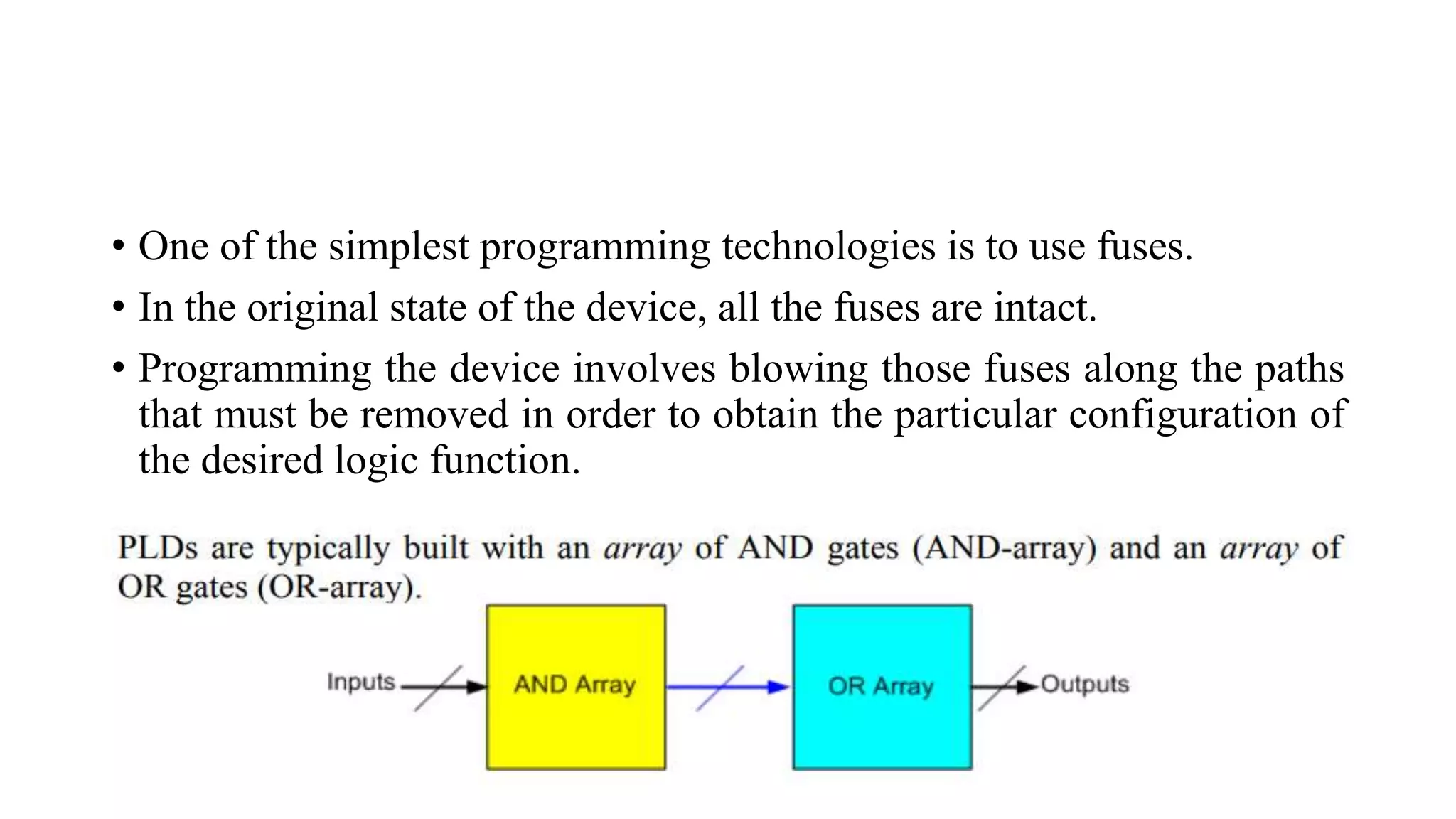
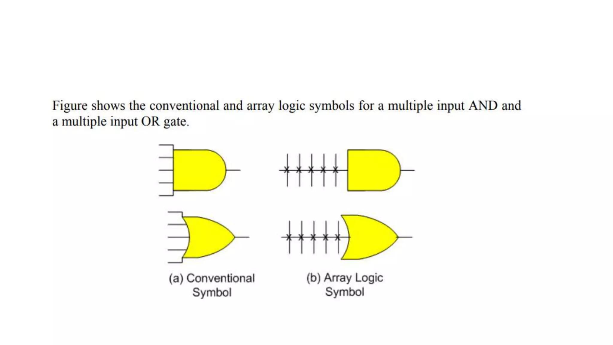
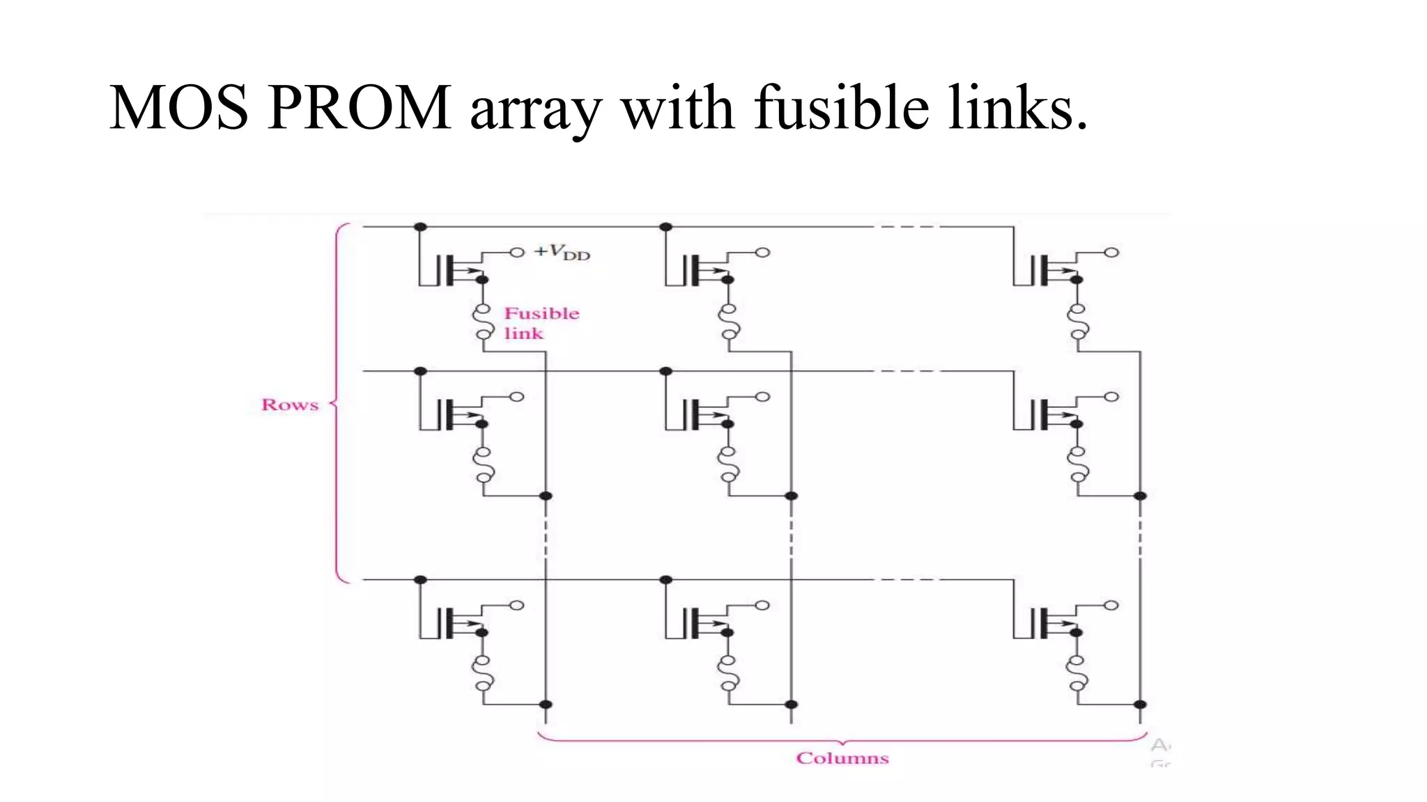
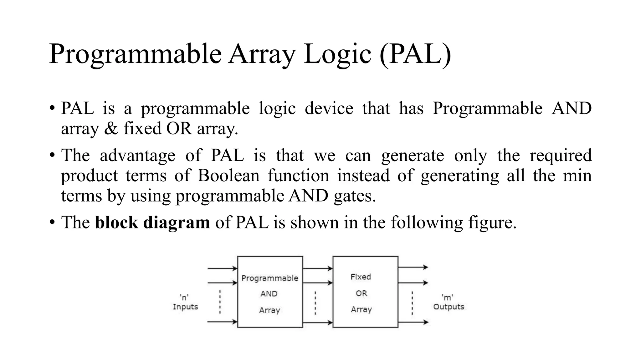
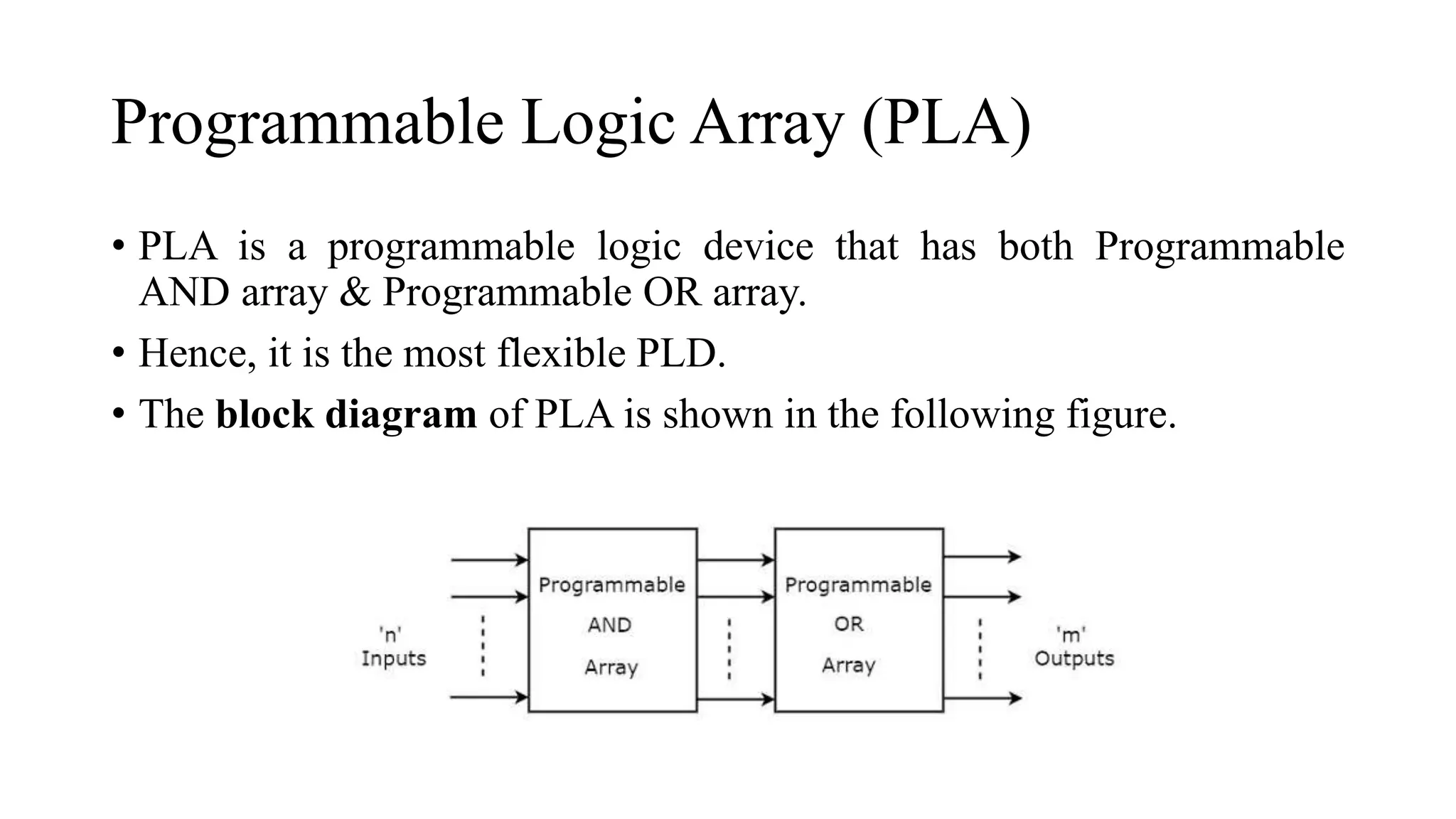
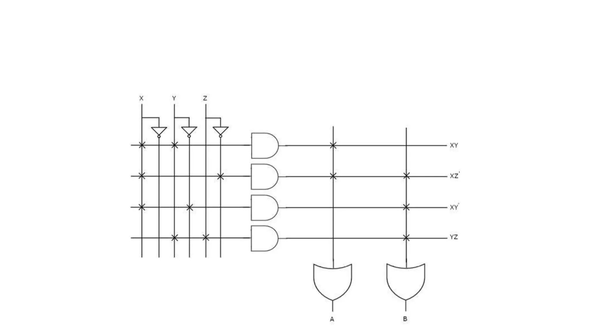
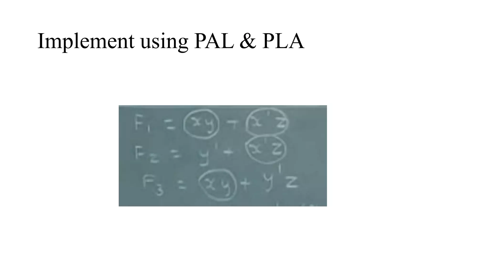
SlideShare a Scribd company logo
Programmable Logic
Devices
Programmable Logic Device (PLD)
• A logic device is an electronic component which performs a definite
function which is decided at the time of manufacture and will never
change.
• For example, a not gate always inverts the logic level of the input
signal and does/can-do-nothing else.
• On the other hand, Programmable Logic Devices (PLDs) are the
components which do not have a specific function associated with
them.
• These can be configured to perform a certain function by the user, on a
need basis and can further be changed to perform some other function
at the later point of time, i.e. these are re-configurable. However, the
amount of flexibility offered depends on their type.
• Programmable Logic Devices (PLDs) are the integrated circuits which
contain an array of AND gates & another array of OR gates.
• The process of entering the information into these devices is known
as programming.
• Here, the term programming refers to hardware programming but not
software programming.
• The internal logic gates AND/OR connections of PLDs can be
changed/configured by a programming process
• One of the simplest programming technologies is to use fuses.
• In the original state of the device, all the fuses are intact.
• Programming the device involves blowing those fuses along the paths
that must be removed in order to obtain the particular configuration of
the desired logic function.
Array logic
• A typical programmable logic device may have hundreds to millions
of gates interconnected through hundreds to thousands of internal
paths.
• In order to show the internal logic diagram in a concise form, it is
necessary to employ a special gate symbology applicable to array
logic.
Types
• Programmable Read Only Memory (PROM)
• Programmable Array Logic (PAL)
• Programmable Logic Array (PLA)
• Assignment : Advantages of using PLDs:
Programmable Read Only Memory (PROM)
• Programmable ROM is a one-time programmable chip that, once
programmed, cannot be erased or altered.
• PROM is also referred as One Time Programmable(OTP)
• These memories are bought in blank form and are programmed using a
special PROM programmer.
• Typically a PROM will consist of an array(collection) of fusible links
some of which are “blown” during the programming process to
provide the required data pattern.
• For every bit of PROM, these exist a fuse. PROM is programmed by
blowing the fuse.
• A typical PROM comes with all bits reading as "1".
• Burning a fuse bit during programming causes the bit to read as "0".
• The memory can be programmed just once after manufacturing by
"blowing" the fuses, which is an irreversible process.
• In the programming process, a sufficient current is injected through
the fusible link to burn it open to create a stored 0. The link is left
intact for a stored 1.
MOS PROM array with fusible links.
• PROM is a programmable logic device that has fixed AND array &
Programmable OR array.
• The block diagram of PROM is shown in the following figure.
• Here, the inputs of AND gates are not of programmable type. So, we
have to generate 2n product terms by using 2n AND gates having n
inputs each. We can implement these product terms by using
nx2n decoder. So, this decoder generates ‘n’ min terms.
• Here, the inputs of OR gates are programmable. That means, we can
program any number of required product terms, since all the outputs of
AND gates are applied as inputs to each OR gate. Therefore, the
outputs of PROM will be in the form of sum of min terms.
Example
• Let us implement the following Boolean functions using PROM
• The given two functions are in sum of min terms form and each
function is having three variables X, Y & Z. So, we require a 3 to 8
decoder and two programmable OR gates for producing these two
functions.
• Here, 3 to 8 decoder generates eight min terms. The two
programmable OR gates have the access of all these min terms.
• But, only the required min terms are programmed in order to produce
the respective Boolean functions by each OR gate.
• The symbol ‘X’ is used for programmable connections.
Home Assignment
Home Assignment
EPROM
• An EPROM is an erasable PROM.
• Unlike an ordinary PROM, an EPROM can be reprogrammed if an
existing program in the memory array is erased first.
• Assignment : Complete the note
Programmable Array Logic (PAL)
• PAL is a programmable logic device that has Programmable AND
array & fixed OR array.
• The advantage of PAL is that we can generate only the required
product terms of Boolean function instead of generating all the min
terms by using programmable AND gates.
• The block diagram of PAL is shown in the following figure.
• Here, the inputs of AND gates are programmable. That means each
AND gate has both normal and complemented inputs of variables. So,
based on the requirement, we can program any of those inputs. So, we
can generate only the required product terms by using these AND
gates.
• Here, the inputs of OR gates are not of programmable type. So, the
number of inputs to each OR gate will be of fixed type. Hence, apply
those required product terms to each OR gate as inputs. Therefore, the
outputs of PAL will be in the form of sum of products form.
Example
• Let us implement the following Boolean functions using PAL
• The given two functions are in sum of products form. There are two
product terms present in each Boolean function. So, we require four
programmable AND gates & two fixed OR gates for producing those
two functions.
• The programmable AND gates have the access of both normal and
complemented inputs of variables.
• So, program only the required literals in order to generate one product
term by each AND gate. The symbol ‘X’ is used for programmable
connections.
• Here, the inputs of OR gates are of fixed type. So, the necessary
product terms are connected to inputs of each OR gate. So that the OR
gates produce the respective Boolean functions. The symbol ‘.’ is used
for fixed connections.
Assignment
• Implementation of full adder using PAL
Programmable Logic Array (PLA)
• PLA is a programmable logic device that has both Programmable
AND array & Programmable OR array.
• Hence, it is the most flexible PLD.
• The block diagram of PLA is shown in the following figure.
• Here, the inputs of AND gates are programmable. That means each
AND gate has both normal and complemented inputs of variables. So,
based on the requirement, we can program any of those inputs. So, we
can generate only the required product terms by using these AND
gates.
• Here, the inputs of OR gates are also programmable. So, we can
program any number of required product terms, since all the outputs of
AND gates are applied as inputs to each OR gate. Therefore, the
outputs of PAL will be in the form of sum of products form.
Example
• Let us implement the following Boolean functions using PLA.
• The given two functions are in sum of products form. The number of
product terms present in the given Boolean functions A & B are two
and three respectively. One product term, is common in each
function.
• So, we require four programmable AND gates & two programmable
OR gates for producing those two functions.
• The programmable AND gates have the access of both normal and
complemented inputs of variables. So, program only the required
literals in order to generate one product term by each AND gate.
• All these product terms are available at the inputs of
each programmable OR gate. But, only program the required
product terms in order to produce the respective Boolean functions by
each OR gate. The symbol ‘X’ is used for programmable connections.
Implement using PAL & PLA
Assignment
• Difference between PLA, PAL and PROM

More Related Content

What's hot

Programmable Logic Array(PLA) & Programmable Array Logic(PAL)
Programmable Logic Array(PLA) & Programmable Array Logic(PAL)Programmable Logic Array(PLA) & Programmable Array Logic(PAL)
Programmable Logic Array(PLA) & Programmable Array Logic(PAL)
Revathi Subramaniam
 
Counters
CountersCounters
Counters
Abhilash Nair
 
Shift Registers
Shift RegistersShift Registers
Shift Registers
Abhilash Nair
 
sequential circuits
sequential circuitssequential circuits
sequential circuits
Unsa Shakir
 
Combinational circuits
Combinational circuits Combinational circuits
Combinational circuits
DrSonali Vyas
 
CMOS Logic Circuits
CMOS Logic CircuitsCMOS Logic Circuits
CMOS Logic Circuits
Marmik Kothari
 
FPGA
FPGAFPGA
programmable logic array
programmable logic arrayprogrammable logic array
programmable logic array
Shiraz Azeem
 
Parity Generator and Parity Checker
Parity Generator and Parity CheckerParity Generator and Parity Checker
Parity Generator and Parity Checker
Jignesh Navdiya
 
digital logic_families
digital logic_familiesdigital logic_families
digital logic_families
Patel Jay
 
Instrumentation amplifier
Instrumentation amplifierInstrumentation amplifier
Instrumentation amplifier
mohdabuzar5
 
Transistor Transistor Logic
Transistor Transistor LogicTransistor Transistor Logic
Transistor Transistor Logic
surat murthy
 
Line codes
Line codesLine codes
Line codes
Madhumita Tamhane
 
Verilog
VerilogVerilog
Verilog
Mohamed Rayan
 
Pass Transistor Logic
Pass Transistor LogicPass Transistor Logic
Pass Transistor Logic
Sudhanshu Janwadkar
 
Nand and nor as a universal gates
Nand and nor as a universal gatesNand and nor as a universal gates
Nand and nor as a universal gates
Kaushal Shah
 
UNIT-II : SEQUENTIAL CIRCUIT DESIGN
UNIT-II  : SEQUENTIAL CIRCUIT DESIGN UNIT-II  : SEQUENTIAL CIRCUIT DESIGN
UNIT-II : SEQUENTIAL CIRCUIT DESIGN
Dr.YNM
 
Stick Diagram
Stick DiagramStick Diagram
Stick Diagram
Kalyan Acharjya
 
UNIT-III-DIGITAL SYSTEM DESIGN
UNIT-III-DIGITAL SYSTEM DESIGNUNIT-III-DIGITAL SYSTEM DESIGN
UNIT-III-DIGITAL SYSTEM DESIGN
Dr.YNM
 
Arithmetic Logic Unit (ALU)
Arithmetic Logic Unit (ALU)Arithmetic Logic Unit (ALU)
Arithmetic Logic Unit (ALU)
Student
 

What's hot (20)

Programmable Logic Array(PLA) & Programmable Array Logic(PAL)
Programmable Logic Array(PLA) & Programmable Array Logic(PAL)Programmable Logic Array(PLA) & Programmable Array Logic(PAL)
Programmable Logic Array(PLA) & Programmable Array Logic(PAL)
 
Counters
CountersCounters
Counters
 
Shift Registers
Shift RegistersShift Registers
Shift Registers
 
sequential circuits
sequential circuitssequential circuits
sequential circuits
 
Combinational circuits
Combinational circuits Combinational circuits
Combinational circuits
 
CMOS Logic Circuits
CMOS Logic CircuitsCMOS Logic Circuits
CMOS Logic Circuits
 
FPGA
FPGAFPGA
FPGA
 
programmable logic array
programmable logic arrayprogrammable logic array
programmable logic array
 
Parity Generator and Parity Checker
Parity Generator and Parity CheckerParity Generator and Parity Checker
Parity Generator and Parity Checker
 
digital logic_families
digital logic_familiesdigital logic_families
digital logic_families
 
Instrumentation amplifier
Instrumentation amplifierInstrumentation amplifier
Instrumentation amplifier
 
Transistor Transistor Logic
Transistor Transistor LogicTransistor Transistor Logic
Transistor Transistor Logic
 
Line codes
Line codesLine codes
Line codes
 
Verilog
VerilogVerilog
Verilog
 
Pass Transistor Logic
Pass Transistor LogicPass Transistor Logic
Pass Transistor Logic
 
Nand and nor as a universal gates
Nand and nor as a universal gatesNand and nor as a universal gates
Nand and nor as a universal gates
 
UNIT-II : SEQUENTIAL CIRCUIT DESIGN
UNIT-II  : SEQUENTIAL CIRCUIT DESIGN UNIT-II  : SEQUENTIAL CIRCUIT DESIGN
UNIT-II : SEQUENTIAL CIRCUIT DESIGN
 
Stick Diagram
Stick DiagramStick Diagram
Stick Diagram
 
UNIT-III-DIGITAL SYSTEM DESIGN
UNIT-III-DIGITAL SYSTEM DESIGNUNIT-III-DIGITAL SYSTEM DESIGN
UNIT-III-DIGITAL SYSTEM DESIGN
 
Arithmetic Logic Unit (ALU)
Arithmetic Logic Unit (ALU)Arithmetic Logic Unit (ALU)
Arithmetic Logic Unit (ALU)
 

Similar to Programmable logic devices

Unit 5 Programmable Logic Devices.pdf
Unit 5 Programmable Logic Devices.pdfUnit 5 Programmable Logic Devices.pdf
Unit 5 Programmable Logic Devices.pdf
SaurabhJaiswal790114
 
Programmable Logic Array
Programmable Logic Array Programmable Logic Array
Programmable Logic Array
Sharun Rajeev
 
PROGRAMMABLE LOGIC DEVICES-PAL, PROM,PLAs
PROGRAMMABLE LOGIC DEVICES-PAL, PROM,PLAsPROGRAMMABLE LOGIC DEVICES-PAL, PROM,PLAs
PROGRAMMABLE LOGIC DEVICES-PAL, PROM,PLAs
DianaD43
 
System design using HDL - Module 3
System design using HDL - Module 3System design using HDL - Module 3
System design using HDL - Module 3
Aravinda Koithyar
 
Unit v memory & programmable logic devices
Unit v   memory & programmable logic devicesUnit v   memory & programmable logic devices
Unit v memory & programmable logic devices
KanmaniRajamanickam
 
module7.pptx
module7.pptxmodule7.pptx
module7.pptx
AMRITRANJAN30
 
siudhai ki marks sheih shuuu kvms jiiiiv
siudhai ki marks sheih shuuu kvms jiiiivsiudhai ki marks sheih shuuu kvms jiiiiv
siudhai ki marks sheih shuuu kvms jiiiiv
wonderboystarpope
 
UNIT I- CPLD & FPGA ARCHITECTURE & APPLICATIONS
UNIT I- CPLD & FPGA ARCHITECTURE & APPLICATIONSUNIT I- CPLD & FPGA ARCHITECTURE & APPLICATIONS
UNIT I- CPLD & FPGA ARCHITECTURE & APPLICATIONS
Dr.YNM
 
Lab 2Lab ObjectivesThe objective for this lab is to review.docx
Lab 2Lab ObjectivesThe objective for this lab is to review.docxLab 2Lab ObjectivesThe objective for this lab is to review.docx
Lab 2Lab ObjectivesThe objective for this lab is to review.docx
DIPESH30
 
EC8392 -DIGITAL ELECTRONICS -II YEAR ECE-by S.SESHA VIDHYA /ASP/ ECE/ RMKCET
EC8392 -DIGITAL ELECTRONICS -II YEAR ECE-by S.SESHA VIDHYA /ASP/ ECE/ RMKCETEC8392 -DIGITAL ELECTRONICS -II YEAR ECE-by S.SESHA VIDHYA /ASP/ ECE/ RMKCET
EC8392 -DIGITAL ELECTRONICS -II YEAR ECE-by S.SESHA VIDHYA /ASP/ ECE/ RMKCET
SeshaVidhyaS
 
Programmable logic array (pla)
Programmable logic array (pla)Programmable logic array (pla)
Programmable logic array (pla)
Zainab Noor
 
Memories in digital electronics
Memories in digital electronicsMemories in digital electronics
Memories in digital electronics
SijuGeorge10
 
Digital Devices Parcial 1 PLD, CPLD, SPLD, FPGA.pptx
Digital Devices Parcial 1 PLD, CPLD, SPLD, FPGA.pptxDigital Devices Parcial 1 PLD, CPLD, SPLD, FPGA.pptx
Digital Devices Parcial 1 PLD, CPLD, SPLD, FPGA.pptx
FilibertoMoralesGarc
 
Lecture syn 024.cpld-fpga
Lecture syn 024.cpld-fpgaLecture syn 024.cpld-fpga
Lecture syn 024.cpld-fpga
Srikanth Pasumarthy
 
Introduction to the Arduino
Introduction to the ArduinoIntroduction to the Arduino
Introduction to the ArduinoWingston
 
COMBINATIONAL PLD-BASED STATE MACHINES
COMBINATIONAL PLD-BASED STATE MACHINESCOMBINATIONAL PLD-BASED STATE MACHINES
COMBINATIONAL PLD-BASED STATE MACHINESdaxesh chauhan
 
Programmable logic array
Programmable logic arrayProgrammable logic array
Programmable logic array
RSARANYADEVI
 
introductiontoarduino-111120102058-phpapp02.pdf
introductiontoarduino-111120102058-phpapp02.pdfintroductiontoarduino-111120102058-phpapp02.pdf
introductiontoarduino-111120102058-phpapp02.pdf
HebaEng
 
Training PPT s.pptx
Training PPT s.pptxTraining PPT s.pptx
Training PPT s.pptx
HarshvarrdhanSolanki
 

Similar to Programmable logic devices (20)

Unit 5 Programmable Logic Devices.pdf
Unit 5 Programmable Logic Devices.pdfUnit 5 Programmable Logic Devices.pdf
Unit 5 Programmable Logic Devices.pdf
 
Programmable Logic Array
Programmable Logic Array Programmable Logic Array
Programmable Logic Array
 
PROGRAMMABLE LOGIC DEVICES-PAL, PROM,PLAs
PROGRAMMABLE LOGIC DEVICES-PAL, PROM,PLAsPROGRAMMABLE LOGIC DEVICES-PAL, PROM,PLAs
PROGRAMMABLE LOGIC DEVICES-PAL, PROM,PLAs
 
System design using HDL - Module 3
System design using HDL - Module 3System design using HDL - Module 3
System design using HDL - Module 3
 
Unit v memory & programmable logic devices
Unit v   memory & programmable logic devicesUnit v   memory & programmable logic devices
Unit v memory & programmable logic devices
 
module7.pptx
module7.pptxmodule7.pptx
module7.pptx
 
siudhai ki marks sheih shuuu kvms jiiiiv
siudhai ki marks sheih shuuu kvms jiiiivsiudhai ki marks sheih shuuu kvms jiiiiv
siudhai ki marks sheih shuuu kvms jiiiiv
 
UNIT I- CPLD & FPGA ARCHITECTURE & APPLICATIONS
UNIT I- CPLD & FPGA ARCHITECTURE & APPLICATIONSUNIT I- CPLD & FPGA ARCHITECTURE & APPLICATIONS
UNIT I- CPLD & FPGA ARCHITECTURE & APPLICATIONS
 
Lab 2Lab ObjectivesThe objective for this lab is to review.docx
Lab 2Lab ObjectivesThe objective for this lab is to review.docxLab 2Lab ObjectivesThe objective for this lab is to review.docx
Lab 2Lab ObjectivesThe objective for this lab is to review.docx
 
EC8392 -DIGITAL ELECTRONICS -II YEAR ECE-by S.SESHA VIDHYA /ASP/ ECE/ RMKCET
EC8392 -DIGITAL ELECTRONICS -II YEAR ECE-by S.SESHA VIDHYA /ASP/ ECE/ RMKCETEC8392 -DIGITAL ELECTRONICS -II YEAR ECE-by S.SESHA VIDHYA /ASP/ ECE/ RMKCET
EC8392 -DIGITAL ELECTRONICS -II YEAR ECE-by S.SESHA VIDHYA /ASP/ ECE/ RMKCET
 
Programmable logic array (pla)
Programmable logic array (pla)Programmable logic array (pla)
Programmable logic array (pla)
 
Memories in digital electronics
Memories in digital electronicsMemories in digital electronics
Memories in digital electronics
 
Digital Devices Parcial 1 PLD, CPLD, SPLD, FPGA.pptx
Digital Devices Parcial 1 PLD, CPLD, SPLD, FPGA.pptxDigital Devices Parcial 1 PLD, CPLD, SPLD, FPGA.pptx
Digital Devices Parcial 1 PLD, CPLD, SPLD, FPGA.pptx
 
Lecture syn 024.cpld-fpga
Lecture syn 024.cpld-fpgaLecture syn 024.cpld-fpga
Lecture syn 024.cpld-fpga
 
Introduction to the Arduino
Introduction to the ArduinoIntroduction to the Arduino
Introduction to the Arduino
 
COMBINATIONAL PLD-BASED STATE MACHINES
COMBINATIONAL PLD-BASED STATE MACHINESCOMBINATIONAL PLD-BASED STATE MACHINES
COMBINATIONAL PLD-BASED STATE MACHINES
 
Programmable logic array
Programmable logic arrayProgrammable logic array
Programmable logic array
 
MPI n OpenMP
MPI n OpenMPMPI n OpenMP
MPI n OpenMP
 
introductiontoarduino-111120102058-phpapp02.pdf
introductiontoarduino-111120102058-phpapp02.pdfintroductiontoarduino-111120102058-phpapp02.pdf
introductiontoarduino-111120102058-phpapp02.pdf
 
Training PPT s.pptx
Training PPT s.pptxTraining PPT s.pptx
Training PPT s.pptx
 

More from ISMT College

Attack.pptx
Attack.pptxAttack.pptx
Attack.pptx
ISMT College
 
Time delays & counter.ppt
Time delays & counter.pptTime delays & counter.ppt
Time delays & counter.ppt
ISMT College
 
Timing Diagram.pptx
Timing Diagram.pptxTiming Diagram.pptx
Timing Diagram.pptx
ISMT College
 
4. Instruction Set Of MP 8085.pptx
4. Instruction Set Of MP 8085.pptx4. Instruction Set Of MP 8085.pptx
4. Instruction Set Of MP 8085.pptx
ISMT College
 
Instruction.pdf
Instruction.pdfInstruction.pdf
Instruction.pdf
ISMT College
 
3. Addressing Modes in 8085 microprocessor.pptx
3. Addressing Modes in 8085 microprocessor.pptx3. Addressing Modes in 8085 microprocessor.pptx
3. Addressing Modes in 8085 microprocessor.pptx
ISMT College
 
2. 8085-Microprocessor.pptx
2. 8085-Microprocessor.pptx2. 8085-Microprocessor.pptx
2. 8085-Microprocessor.pptx
ISMT College
 
1. Introduction to Microprocessor.pptx
1. Introduction to Microprocessor.pptx1. Introduction to Microprocessor.pptx
1. Introduction to Microprocessor.pptx
ISMT College
 
Digital Logic BCA TU Chapter 2.2
Digital Logic BCA TU Chapter 2.2Digital Logic BCA TU Chapter 2.2
Digital Logic BCA TU Chapter 2.2
ISMT College
 
Chapter 1 Introduction to Digital Logic
Chapter 1 Introduction to Digital LogicChapter 1 Introduction to Digital Logic
Chapter 1 Introduction to Digital Logic
ISMT College
 
VLAN
VLANVLAN
Access Control List (ACL)
Access Control List (ACL)Access Control List (ACL)
Access Control List (ACL)
ISMT College
 
Introduction to Counters
Introduction to CountersIntroduction to Counters
Introduction to Counters
ISMT College
 
Chapter 2.1 introduction to number system
Chapter 2.1 introduction to number systemChapter 2.1 introduction to number system
Chapter 2.1 introduction to number system
ISMT College
 
Chapter 1 Introduction to Digital Logic
Chapter 1 Introduction to Digital LogicChapter 1 Introduction to Digital Logic
Chapter 1 Introduction to Digital Logic
ISMT College
 
Basic Gates in Digital Logic
Basic Gates in Digital LogicBasic Gates in Digital Logic
Basic Gates in Digital Logic
ISMT College
 
Adder & subtractor (Half adder, Full adder, Half subtractor, Full subtractor)
Adder & subtractor (Half adder, Full adder, Half subtractor, Full subtractor)Adder & subtractor (Half adder, Full adder, Half subtractor, Full subtractor)
Adder & subtractor (Half adder, Full adder, Half subtractor, Full subtractor)
ISMT College
 
Register in Digital Logic
Register in Digital LogicRegister in Digital Logic
Register in Digital Logic
ISMT College
 

More from ISMT College (18)

Attack.pptx
Attack.pptxAttack.pptx
Attack.pptx
 
Time delays & counter.ppt
Time delays & counter.pptTime delays & counter.ppt
Time delays & counter.ppt
 
Timing Diagram.pptx
Timing Diagram.pptxTiming Diagram.pptx
Timing Diagram.pptx
 
4. Instruction Set Of MP 8085.pptx
4. Instruction Set Of MP 8085.pptx4. Instruction Set Of MP 8085.pptx
4. Instruction Set Of MP 8085.pptx
 
Instruction.pdf
Instruction.pdfInstruction.pdf
Instruction.pdf
 
3. Addressing Modes in 8085 microprocessor.pptx
3. Addressing Modes in 8085 microprocessor.pptx3. Addressing Modes in 8085 microprocessor.pptx
3. Addressing Modes in 8085 microprocessor.pptx
 
2. 8085-Microprocessor.pptx
2. 8085-Microprocessor.pptx2. 8085-Microprocessor.pptx
2. 8085-Microprocessor.pptx
 
1. Introduction to Microprocessor.pptx
1. Introduction to Microprocessor.pptx1. Introduction to Microprocessor.pptx
1. Introduction to Microprocessor.pptx
 
Digital Logic BCA TU Chapter 2.2
Digital Logic BCA TU Chapter 2.2Digital Logic BCA TU Chapter 2.2
Digital Logic BCA TU Chapter 2.2
 
Chapter 1 Introduction to Digital Logic
Chapter 1 Introduction to Digital LogicChapter 1 Introduction to Digital Logic
Chapter 1 Introduction to Digital Logic
 
VLAN
VLANVLAN
VLAN
 
Access Control List (ACL)
Access Control List (ACL)Access Control List (ACL)
Access Control List (ACL)
 
Introduction to Counters
Introduction to CountersIntroduction to Counters
Introduction to Counters
 
Chapter 2.1 introduction to number system
Chapter 2.1 introduction to number systemChapter 2.1 introduction to number system
Chapter 2.1 introduction to number system
 
Chapter 1 Introduction to Digital Logic
Chapter 1 Introduction to Digital LogicChapter 1 Introduction to Digital Logic
Chapter 1 Introduction to Digital Logic
 
Basic Gates in Digital Logic
Basic Gates in Digital LogicBasic Gates in Digital Logic
Basic Gates in Digital Logic
 
Adder & subtractor (Half adder, Full adder, Half subtractor, Full subtractor)
Adder & subtractor (Half adder, Full adder, Half subtractor, Full subtractor)Adder & subtractor (Half adder, Full adder, Half subtractor, Full subtractor)
Adder & subtractor (Half adder, Full adder, Half subtractor, Full subtractor)
 
Register in Digital Logic
Register in Digital LogicRegister in Digital Logic
Register in Digital Logic
 

Recently uploaded

AP LAB PPT.pdf ap lab ppt no title specific
AP LAB PPT.pdf ap lab ppt no title specificAP LAB PPT.pdf ap lab ppt no title specific
AP LAB PPT.pdf ap lab ppt no title specific
BrazilAccount1
 
CME397 Surface Engineering- Professional Elective
CME397 Surface Engineering- Professional ElectiveCME397 Surface Engineering- Professional Elective
CME397 Surface Engineering- Professional Elective
karthi keyan
 
Water Industry Process Automation and Control Monthly - May 2024.pdf
Water Industry Process Automation and Control Monthly - May 2024.pdfWater Industry Process Automation and Control Monthly - May 2024.pdf
Water Industry Process Automation and Control Monthly - May 2024.pdf
Water Industry Process Automation & Control
 
DESIGN A COTTON SEED SEPARATION MACHINE.docx
DESIGN A COTTON SEED SEPARATION MACHINE.docxDESIGN A COTTON SEED SEPARATION MACHINE.docx
DESIGN A COTTON SEED SEPARATION MACHINE.docx
FluxPrime1
 
The Benefits and Techniques of Trenchless Pipe Repair.pdf
The Benefits and Techniques of Trenchless Pipe Repair.pdfThe Benefits and Techniques of Trenchless Pipe Repair.pdf
The Benefits and Techniques of Trenchless Pipe Repair.pdf
Pipe Restoration Solutions
 
J.Yang, ICLR 2024, MLILAB, KAIST AI.pdf
J.Yang,  ICLR 2024, MLILAB, KAIST AI.pdfJ.Yang,  ICLR 2024, MLILAB, KAIST AI.pdf
J.Yang, ICLR 2024, MLILAB, KAIST AI.pdf
MLILAB
 
Pile Foundation by Venkatesh Taduvai (Sub Geotechnical Engineering II)-conver...
Pile Foundation by Venkatesh Taduvai (Sub Geotechnical Engineering II)-conver...Pile Foundation by Venkatesh Taduvai (Sub Geotechnical Engineering II)-conver...
Pile Foundation by Venkatesh Taduvai (Sub Geotechnical Engineering II)-conver...
AJAYKUMARPUND1
 
block diagram and signal flow graph representation
block diagram and signal flow graph representationblock diagram and signal flow graph representation
block diagram and signal flow graph representation
Divya Somashekar
 
一比一原版(SFU毕业证)西蒙菲莎大学毕业证成绩单如何办理
一比一原版(SFU毕业证)西蒙菲莎大学毕业证成绩单如何办理一比一原版(SFU毕业证)西蒙菲莎大学毕业证成绩单如何办理
一比一原版(SFU毕业证)西蒙菲莎大学毕业证成绩单如何办理
bakpo1
 
road safety engineering r s e unit 3.pdf
road safety engineering  r s e unit 3.pdfroad safety engineering  r s e unit 3.pdf
road safety engineering r s e unit 3.pdf
VENKATESHvenky89705
 
Cosmetic shop management system project report.pdf
Cosmetic shop management system project report.pdfCosmetic shop management system project report.pdf
Cosmetic shop management system project report.pdf
Kamal Acharya
 
Hierarchical Digital Twin of a Naval Power System
Hierarchical Digital Twin of a Naval Power SystemHierarchical Digital Twin of a Naval Power System
Hierarchical Digital Twin of a Naval Power System
Kerry Sado
 
Top 10 Oil and Gas Projects in Saudi Arabia 2024.pdf
Top 10 Oil and Gas Projects in Saudi Arabia 2024.pdfTop 10 Oil and Gas Projects in Saudi Arabia 2024.pdf
Top 10 Oil and Gas Projects in Saudi Arabia 2024.pdf
Teleport Manpower Consultant
 
Fundamentals of Electric Drives and its applications.pptx
Fundamentals of Electric Drives and its applications.pptxFundamentals of Electric Drives and its applications.pptx
Fundamentals of Electric Drives and its applications.pptx
manasideore6
 
RAT: Retrieval Augmented Thoughts Elicit Context-Aware Reasoning in Long-Hori...
RAT: Retrieval Augmented Thoughts Elicit Context-Aware Reasoning in Long-Hori...RAT: Retrieval Augmented Thoughts Elicit Context-Aware Reasoning in Long-Hori...
RAT: Retrieval Augmented Thoughts Elicit Context-Aware Reasoning in Long-Hori...
thanhdowork
 
Nuclear Power Economics and Structuring 2024
Nuclear Power Economics and Structuring 2024Nuclear Power Economics and Structuring 2024
Nuclear Power Economics and Structuring 2024
Massimo Talia
 
Standard Reomte Control Interface - Neometrix
Standard Reomte Control Interface - NeometrixStandard Reomte Control Interface - Neometrix
Standard Reomte Control Interface - Neometrix
Neometrix_Engineering_Pvt_Ltd
 
weather web application report.pdf
weather web application report.pdfweather web application report.pdf
weather web application report.pdf
Pratik Pawar
 
Design and Analysis of Algorithms-DP,Backtracking,Graphs,B&B
Design and Analysis of Algorithms-DP,Backtracking,Graphs,B&BDesign and Analysis of Algorithms-DP,Backtracking,Graphs,B&B
Design and Analysis of Algorithms-DP,Backtracking,Graphs,B&B
Sreedhar Chowdam
 
Runway Orientation Based on the Wind Rose Diagram.pptx
Runway Orientation Based on the Wind Rose Diagram.pptxRunway Orientation Based on the Wind Rose Diagram.pptx
Runway Orientation Based on the Wind Rose Diagram.pptx
SupreethSP4
 

Recently uploaded (20)

AP LAB PPT.pdf ap lab ppt no title specific
AP LAB PPT.pdf ap lab ppt no title specificAP LAB PPT.pdf ap lab ppt no title specific
AP LAB PPT.pdf ap lab ppt no title specific
 
CME397 Surface Engineering- Professional Elective
CME397 Surface Engineering- Professional ElectiveCME397 Surface Engineering- Professional Elective
CME397 Surface Engineering- Professional Elective
 
Water Industry Process Automation and Control Monthly - May 2024.pdf
Water Industry Process Automation and Control Monthly - May 2024.pdfWater Industry Process Automation and Control Monthly - May 2024.pdf
Water Industry Process Automation and Control Monthly - May 2024.pdf
 
DESIGN A COTTON SEED SEPARATION MACHINE.docx
DESIGN A COTTON SEED SEPARATION MACHINE.docxDESIGN A COTTON SEED SEPARATION MACHINE.docx
DESIGN A COTTON SEED SEPARATION MACHINE.docx
 
The Benefits and Techniques of Trenchless Pipe Repair.pdf
The Benefits and Techniques of Trenchless Pipe Repair.pdfThe Benefits and Techniques of Trenchless Pipe Repair.pdf
The Benefits and Techniques of Trenchless Pipe Repair.pdf
 
J.Yang, ICLR 2024, MLILAB, KAIST AI.pdf
J.Yang,  ICLR 2024, MLILAB, KAIST AI.pdfJ.Yang,  ICLR 2024, MLILAB, KAIST AI.pdf
J.Yang, ICLR 2024, MLILAB, KAIST AI.pdf
 
Pile Foundation by Venkatesh Taduvai (Sub Geotechnical Engineering II)-conver...
Pile Foundation by Venkatesh Taduvai (Sub Geotechnical Engineering II)-conver...Pile Foundation by Venkatesh Taduvai (Sub Geotechnical Engineering II)-conver...
Pile Foundation by Venkatesh Taduvai (Sub Geotechnical Engineering II)-conver...
 
block diagram and signal flow graph representation
block diagram and signal flow graph representationblock diagram and signal flow graph representation
block diagram and signal flow graph representation
 
一比一原版(SFU毕业证)西蒙菲莎大学毕业证成绩单如何办理
一比一原版(SFU毕业证)西蒙菲莎大学毕业证成绩单如何办理一比一原版(SFU毕业证)西蒙菲莎大学毕业证成绩单如何办理
一比一原版(SFU毕业证)西蒙菲莎大学毕业证成绩单如何办理
 
road safety engineering r s e unit 3.pdf
road safety engineering  r s e unit 3.pdfroad safety engineering  r s e unit 3.pdf
road safety engineering r s e unit 3.pdf
 
Cosmetic shop management system project report.pdf
Cosmetic shop management system project report.pdfCosmetic shop management system project report.pdf
Cosmetic shop management system project report.pdf
 
Hierarchical Digital Twin of a Naval Power System
Hierarchical Digital Twin of a Naval Power SystemHierarchical Digital Twin of a Naval Power System
Hierarchical Digital Twin of a Naval Power System
 
Top 10 Oil and Gas Projects in Saudi Arabia 2024.pdf
Top 10 Oil and Gas Projects in Saudi Arabia 2024.pdfTop 10 Oil and Gas Projects in Saudi Arabia 2024.pdf
Top 10 Oil and Gas Projects in Saudi Arabia 2024.pdf
 
Fundamentals of Electric Drives and its applications.pptx
Fundamentals of Electric Drives and its applications.pptxFundamentals of Electric Drives and its applications.pptx
Fundamentals of Electric Drives and its applications.pptx
 
RAT: Retrieval Augmented Thoughts Elicit Context-Aware Reasoning in Long-Hori...
RAT: Retrieval Augmented Thoughts Elicit Context-Aware Reasoning in Long-Hori...RAT: Retrieval Augmented Thoughts Elicit Context-Aware Reasoning in Long-Hori...
RAT: Retrieval Augmented Thoughts Elicit Context-Aware Reasoning in Long-Hori...
 
Nuclear Power Economics and Structuring 2024
Nuclear Power Economics and Structuring 2024Nuclear Power Economics and Structuring 2024
Nuclear Power Economics and Structuring 2024
 
Standard Reomte Control Interface - Neometrix
Standard Reomte Control Interface - NeometrixStandard Reomte Control Interface - Neometrix
Standard Reomte Control Interface - Neometrix
 
weather web application report.pdf
weather web application report.pdfweather web application report.pdf
weather web application report.pdf
 
Design and Analysis of Algorithms-DP,Backtracking,Graphs,B&B
Design and Analysis of Algorithms-DP,Backtracking,Graphs,B&BDesign and Analysis of Algorithms-DP,Backtracking,Graphs,B&B
Design and Analysis of Algorithms-DP,Backtracking,Graphs,B&B
 
Runway Orientation Based on the Wind Rose Diagram.pptx
Runway Orientation Based on the Wind Rose Diagram.pptxRunway Orientation Based on the Wind Rose Diagram.pptx
Runway Orientation Based on the Wind Rose Diagram.pptx
 

Programmable logic devices

  • 2. Programmable Logic Device (PLD) • A logic device is an electronic component which performs a definite function which is decided at the time of manufacture and will never change. • For example, a not gate always inverts the logic level of the input signal and does/can-do-nothing else. • On the other hand, Programmable Logic Devices (PLDs) are the components which do not have a specific function associated with them. • These can be configured to perform a certain function by the user, on a need basis and can further be changed to perform some other function at the later point of time, i.e. these are re-configurable. However, the amount of flexibility offered depends on their type.
  • 3. • Programmable Logic Devices (PLDs) are the integrated circuits which contain an array of AND gates & another array of OR gates. • The process of entering the information into these devices is known as programming. • Here, the term programming refers to hardware programming but not software programming. • The internal logic gates AND/OR connections of PLDs can be changed/configured by a programming process
  • 4. • One of the simplest programming technologies is to use fuses. • In the original state of the device, all the fuses are intact. • Programming the device involves blowing those fuses along the paths that must be removed in order to obtain the particular configuration of the desired logic function.
  • 5. Array logic • A typical programmable logic device may have hundreds to millions of gates interconnected through hundreds to thousands of internal paths. • In order to show the internal logic diagram in a concise form, it is necessary to employ a special gate symbology applicable to array logic.
  • 6.
  • 7. Types • Programmable Read Only Memory (PROM) • Programmable Array Logic (PAL) • Programmable Logic Array (PLA) • Assignment : Advantages of using PLDs:
  • 8. Programmable Read Only Memory (PROM) • Programmable ROM is a one-time programmable chip that, once programmed, cannot be erased or altered. • PROM is also referred as One Time Programmable(OTP) • These memories are bought in blank form and are programmed using a special PROM programmer. • Typically a PROM will consist of an array(collection) of fusible links some of which are “blown” during the programming process to provide the required data pattern. • For every bit of PROM, these exist a fuse. PROM is programmed by blowing the fuse.
  • 9. • A typical PROM comes with all bits reading as "1". • Burning a fuse bit during programming causes the bit to read as "0". • The memory can be programmed just once after manufacturing by "blowing" the fuses, which is an irreversible process. • In the programming process, a sufficient current is injected through the fusible link to burn it open to create a stored 0. The link is left intact for a stored 1.
  • 10. MOS PROM array with fusible links.
  • 11. • PROM is a programmable logic device that has fixed AND array & Programmable OR array. • The block diagram of PROM is shown in the following figure.
  • 12. • Here, the inputs of AND gates are not of programmable type. So, we have to generate 2n product terms by using 2n AND gates having n inputs each. We can implement these product terms by using nx2n decoder. So, this decoder generates ‘n’ min terms. • Here, the inputs of OR gates are programmable. That means, we can program any number of required product terms, since all the outputs of AND gates are applied as inputs to each OR gate. Therefore, the outputs of PROM will be in the form of sum of min terms.
  • 13. Example • Let us implement the following Boolean functions using PROM • The given two functions are in sum of min terms form and each function is having three variables X, Y & Z. So, we require a 3 to 8 decoder and two programmable OR gates for producing these two functions.
  • 14.
  • 15. • Here, 3 to 8 decoder generates eight min terms. The two programmable OR gates have the access of all these min terms. • But, only the required min terms are programmed in order to produce the respective Boolean functions by each OR gate. • The symbol ‘X’ is used for programmable connections.
  • 18. EPROM • An EPROM is an erasable PROM. • Unlike an ordinary PROM, an EPROM can be reprogrammed if an existing program in the memory array is erased first. • Assignment : Complete the note
  • 19. Programmable Array Logic (PAL) • PAL is a programmable logic device that has Programmable AND array & fixed OR array. • The advantage of PAL is that we can generate only the required product terms of Boolean function instead of generating all the min terms by using programmable AND gates. • The block diagram of PAL is shown in the following figure.
  • 20. • Here, the inputs of AND gates are programmable. That means each AND gate has both normal and complemented inputs of variables. So, based on the requirement, we can program any of those inputs. So, we can generate only the required product terms by using these AND gates. • Here, the inputs of OR gates are not of programmable type. So, the number of inputs to each OR gate will be of fixed type. Hence, apply those required product terms to each OR gate as inputs. Therefore, the outputs of PAL will be in the form of sum of products form.
  • 21. Example • Let us implement the following Boolean functions using PAL • The given two functions are in sum of products form. There are two product terms present in each Boolean function. So, we require four programmable AND gates & two fixed OR gates for producing those two functions.
  • 22.
  • 23. • The programmable AND gates have the access of both normal and complemented inputs of variables. • So, program only the required literals in order to generate one product term by each AND gate. The symbol ‘X’ is used for programmable connections. • Here, the inputs of OR gates are of fixed type. So, the necessary product terms are connected to inputs of each OR gate. So that the OR gates produce the respective Boolean functions. The symbol ‘.’ is used for fixed connections.
  • 24. Assignment • Implementation of full adder using PAL
  • 25. Programmable Logic Array (PLA) • PLA is a programmable logic device that has both Programmable AND array & Programmable OR array. • Hence, it is the most flexible PLD. • The block diagram of PLA is shown in the following figure.
  • 26. • Here, the inputs of AND gates are programmable. That means each AND gate has both normal and complemented inputs of variables. So, based on the requirement, we can program any of those inputs. So, we can generate only the required product terms by using these AND gates. • Here, the inputs of OR gates are also programmable. So, we can program any number of required product terms, since all the outputs of AND gates are applied as inputs to each OR gate. Therefore, the outputs of PAL will be in the form of sum of products form.
  • 27. Example • Let us implement the following Boolean functions using PLA. • The given two functions are in sum of products form. The number of product terms present in the given Boolean functions A & B are two and three respectively. One product term, is common in each function. • So, we require four programmable AND gates & two programmable OR gates for producing those two functions.
  • 28.
  • 29. • The programmable AND gates have the access of both normal and complemented inputs of variables. So, program only the required literals in order to generate one product term by each AND gate. • All these product terms are available at the inputs of each programmable OR gate. But, only program the required product terms in order to produce the respective Boolean functions by each OR gate. The symbol ‘X’ is used for programmable connections.