This document provides a summary of a book about PCI Express technology. It includes an introduction to the book, a table of contents listing the topics covered, biographies of the authors, and endorsements of the book. The summary is as follows:
The document introduces a book that provides a comprehensive guide to PCI Express generations 1.x, 2.x, and 3.0. It includes biographies of the authors and an endorsement quoting that the book is essential for understanding PCI Express. The table of contents indicates it will cover topics such as the origins and architecture of PCI Express, various technical specifications and features, and considerations for high-speed signaling.


![Many of the designations used by manufacturers and sellers to distinguish their prod‐
ucts are claimed as trademarks. Where those designators appear in this book, and
MindShare was aware of the trademark claim, the designations have been printed in ini‐
tial capital letters or all capital letters.
The authors and publishers have taken care in preparation of this book, but make no
expressed or implied warranty of any kind and assume no responsibility for errors or
omissions. No liability is assumed for incidental or consequential damages in connec‐
tion with or arising out of the use of the information or programs contained herein.
Library of Congress Cataloging‐in‐Publication Data
Jackson, Mike and Budruk, Ravi
PCI Express Technology / MindShare, Inc., Mike Jackson, Ravi Budruk....[et al.]
Includes index
ISBN: 978‐0‐9836465‐2‐5 (alk. paper)
1. Computer Architecture. 2.0 Microcomputers ‐ buses.
I. Jackson, Mike II. MindShare, Inc. III. Title
Library of Congress Number: 2011921066
ISBN: 978‐0‐9836465‐2‐5
Copyright ©2012 by MindShare, Inc.
All rights reserved. No part of this publication may be reproduced, stored in a retrieval
system, or transmitted, in any form or by any means, electronic, mechanical, photocopy‐
ing, recording, or otherwise, without the prior written permission of the publisher.
Printed in the United States of America.
Editors: Joe Winkles and Don Anderson
Project Manager: Maryanne Daves
Cover Design: Greenhouse Creative and MindShare, Inc.
Set in 10 point Palatino Linotype by MindShare, Inc.
Text printed on recycled and acid‐free paper
First Edition, First Printing, September, 2012
PCIe 3.0.book Page ii Sunday, September 2, 2012 11:25 AM](https://image.slidesharecdn.com/pciexpresstechnology3-161107170938/85/Pci-express-technology-3-0-7-320.jpg)


![Contents
xxv
Phase 2 Upstream .............................................................................................. 593
Phase 3 Upstream .............................................................................................. 594
Recovery.Speed......................................................................................................... 595
Recovery.RcvrCfg..................................................................................................... 598
Recovery.Idle............................................................................................................. 601
L0s State............................................................................................................................. 603
L0s Transmitter State Machine ............................................................................... 603
Tx_L0s.Entry....................................................................................................... 604
Tx_L0s.Idle.......................................................................................................... 604
Tx_L0s.FTS.......................................................................................................... 604
L0s Receiver State Machine..................................................................................... 605
Rx_L0s.Entry ...................................................................................................... 606
Rx_L0s.Idle ......................................................................................................... 606
Rx_L0s.FTS ......................................................................................................... 606
L1 State .............................................................................................................................. 607
L1.Entry...................................................................................................................... 608
L1.Idle......................................................................................................................... 609
L2 State .............................................................................................................................. 609
L2.Idle......................................................................................................................... 611
L2.TransmitWake...................................................................................................... 612
Hot Reset State.................................................................................................................. 612
Disable State...................................................................................................................... 613
Loopback State ................................................................................................................. 613
Loopback.Entry......................................................................................................... 614
Loopback.Active ....................................................................................................... 617
Loopback.Exit............................................................................................................ 618
Dynamic Bandwidth Changes............................................................................................. 618
Dynamic Link Speed Changes....................................................................................... 619
Upstream Port Initiates Speed Change......................................................................... 622
Speed Change Example................................................................................................... 622
Software Control of Speed Changes.............................................................................. 627
Dynamic Link Width Changes....................................................................................... 629
Link Width Change Example......................................................................................... 630
Related Configuration Registers......................................................................................... 638
Link Capabilities Register............................................................................................... 638
Max Link Speed [3:0]................................................................................................ 639
Maximum Link Width[9:4]...................................................................................... 640
Link Capabilities 2 Register............................................................................................ 640
Link Status Register......................................................................................................... 641
Current Link Speed[3:0]:.......................................................................................... 641
Negotiated Link Width[9:4] .................................................................................... 641
Undefined[10]............................................................................................................ 642
PCIe 3.0.book Page xxv Sunday, September 2, 2012 11:25 AM](https://image.slidesharecdn.com/pciexpresstechnology3-161107170938/85/Pci-express-technology-3-0-30-320.jpg)
![Contents
xxvi
Link Training[11] ...................................................................................................... 642
Link Control Register ...................................................................................................... 642
Link Disable............................................................................................................... 643
Retrain Link ............................................................................................................... 643
Extended Synch......................................................................................................... 643
Part Five: Additional System Topics
Chapter 15: Error Detection and Handling
Background ............................................................................................................................. 648
PCIe Error Definitions .......................................................................................................... 650
PCIe Error Reporting............................................................................................................. 650
Baseline Error Reporting................................................................................................. 650
Advanced Error Reporting (AER) ................................................................................. 651
Error Classes............................................................................................................................ 651
Correctable Errors............................................................................................................ 651
Uncorrectable Errors........................................................................................................ 652
Non-fatal Uncorrectable Errors .............................................................................. 652
Fatal Uncorrectable Errors....................................................................................... 652
PCIe Error Checking Mechanisms...................................................................................... 652
CRC .................................................................................................................................... 653
Error Checks by Layer..................................................................................................... 655
Physical Layer Errors ............................................................................................... 655
Data Link Layer Errors ............................................................................................ 655
Transaction Layer Errors ......................................................................................... 656
Error Pollution ........................................................................................................................ 656
Sources of PCI Express Errors.............................................................................................. 657
ECRC Generation and Checking ................................................................................... 657
TLP Digest.................................................................................................................. 659
Variant Bits Not Included in ECRC Mechanism.................................................. 659
Data Poisoning ................................................................................................................. 660
Split Transaction Errors .................................................................................................. 662
Unsupported Request (UR) Status......................................................................... 663
Completer Abort (CA) Status.................................................................................. 664
Unexpected Completion.......................................................................................... 664
Completion Timeout ................................................................................................ 665
Link Flow Control Related Errors ................................................................................. 666
Malformed TLP ................................................................................................................ 666
Internal Errors .................................................................................................................. 667
The Problem............................................................................................................... 667
The Solution............................................................................................................... 668
PCIe 3.0.book Page xxvi Sunday, September 2, 2012 11:25 AM](https://image.slidesharecdn.com/pciexpresstechnology3-161107170938/85/Pci-express-technology-3-0-31-320.jpg)


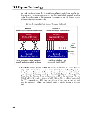
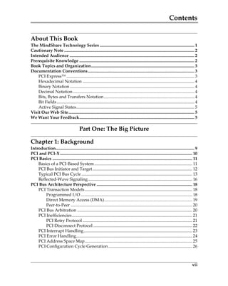
![PCI Express Technology
4
Hexadecimal Notation
All hex numbers are followed by a lower case “h.” For example:
89F2BD02h
0111h
Binary Notation
All binary numbers are followed by a lower case “b.” For example:
1000 1001 1111 0010b
01b
Decimal Notation
Number without any suffix are decimal. When required for clarity, decimal
numbers are followed by a lower case “d.” Examples:
9
15
512d
Bits, Bytes and Transfers Notation
This book represents bits with a lower‐case “b” and bytes with an upper‐case
“B.” For example:
Megabits/second = Mb/s
Megabytes/second = MB/s
Megatransfers/second = MT/s
Bit Fields
Groups bits are represented with the high‐order bits first followed by the low‐
order bits and enclosed by brackets. For example:
[7:0] = bits 0 through 7
PCIe 3.0.book Page 4 Sunday, September 2, 2012 11:25 AM](https://image.slidesharecdn.com/pciexpresstechnology3-161107170938/85/Pci-express-technology-3-0-63-320.jpg)


![Chapter 7: Quality of Service
247
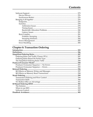
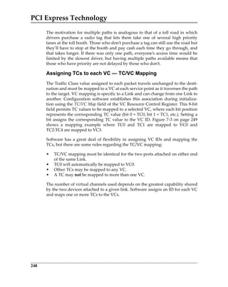
Traffic Class (TC)
The first thing we need is a way to differentiate traffic; something to distinguish
which packets have high priority. This is accomplished by designating Traffic
Classes (TCs) that define eight priorities specified by a 3‐bit TC field within each
TLP header (with ascending priority; TC 0‐7). The 32‐bit memory request
header in Figure 7‐2 reveals the location of the TC field. During initialization,
the device driver communicates the level of services to the isochronous man‐
agement software, which returns the appropriate TC values to use for each type
of packet. The driver then assigns the correct TC priority for the packet. The TC
value defaults to zero so packets that don’t need priority service won’t acciden‐
tally interfere with those that do.
Configuration software that’s unaware of PCIe won’t recognize the new regis‐
ters and will use the default TC0/VC0 combination for all transactions. In addi‐
tion, there are some packets that are always required to use TC0/VC0, including
Configuration, I/O, and Message transactions. If these packets are thought of as
maintenance‐level traffic, then it makes sense that they would need to be con‐
fined to VC0 and kept out of the path of high‐priority packets.
Virtual Channels (VCs)
VCs are hardware buffers that act as queues for outgoing packets. Each port
must include the default VC0, but may have as many as eight (from VC0 to
VC7). Each channel represents a different path available for outgoing packets.
Figure 7‐2: Traffic Class Field in TLP Header
Byte 0
Byte 4
Byte 8
+3
7 6 5 4 3 2 1 07 6 5 4 3 2 1 07 6 5 4 3 2 1 07 6 5 4 3 2 1 0
+2+1+0
LengthATTCType
Requester ID Tag
Address [31:2]
Fmt R
R
RR E
P
1st DW
BE
Last DW
BE
T
D
T
H
At
tr
Attr
PCIe 3.0.book Page 247 Sunday, September 2, 2012 11:25 AM](https://image.slidesharecdn.com/pciexpresstechnology3-161107170938/85/Pci-express-technology-3-0-96-320.jpg)

![PCI Express Technology
320
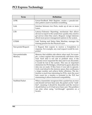
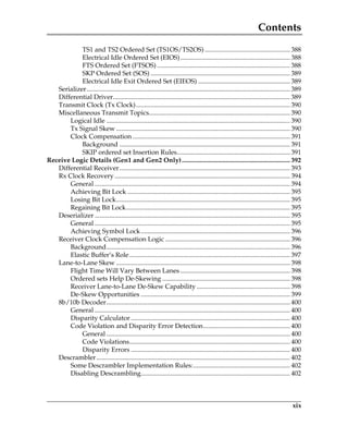
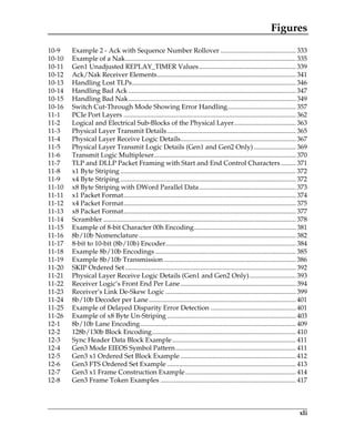
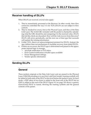
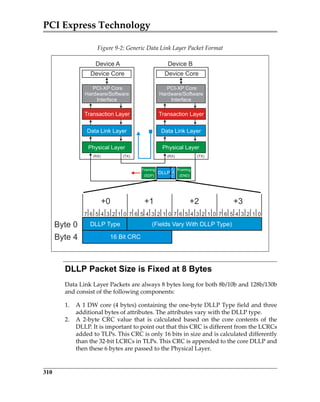
Elements of the Ack/Nak Protocol
The major Ack/Nak protocol elements of the Data Link Layer are shown in Fig‐
ure 10‐3 on page 320. There’s too much to consider all at once, though, so let’s
begin by focusing on just the transmitter elements, which are shown in a larger
view in Figure 10‐4 on page 322.
Transmitter Elements
As TLPs arrive from the Transaction Layer, several things are done to prepare
them for robust error detection at the receiver. As shown in the diagram TLPs
are first assigned the next sequential Sequence Number, obtained from the 12‐
bit NEXT_TRANSMIT_SEQ counter.
Figure 10‐3: Elements of the Ack/Nak Protocol
Seq Num NRS (Duplicate TLP)
DLLP
Ack/Nak
TLPTLP
Ack/Nak
Generator
NEXT_RCV_SEQ (NRS)
Increment NRS
Seq Num = NRS
NAK_SCHEDULED
Yes
Nak
Seq Num NRS (Lost TLP)
(Schedule Ack)
AckNak Latency
Timer
Nak Flag Clear?
Set Send Nak
Transaction Layer (RX)
Good TLPs
Good TLP?
Pass
LCRC?
Seq Num
, , =
NRS?
No
Assign
Sequence
Number
NEXT_TRANSMIT_SEQ (NTS)
LCRC
Generator
(Increment)
Yes
No
(Discard)
REPLAY_NUM
REPLAY_TIMER
(Reset Both)
BlockTLPduringReplay
No
Transaction Layer (TX) Block TLPs; Report
DLL protocol error
AckD_SEQ (AS)
No
Purge Older TLPs
Yes
Increment on Replay)
Pass
CRC?
(NTS-AS) ≥ 2048?
Nak?
Nak
Yes
(Replay)
Retry (Replay)
Buffer
(TLP copy)
(Update)
(TLP copy)
(Continue)
Yes
(Send Nak)
(Send Nak)
Ack
Clear Nak Flag
AckNak
SeqNum = AS?
Link
TLPs
(NRS–1)=AckNak_Seq_Num[11:0]
PCIe 3.0.book Page 320 Sunday, September 2, 2012 11:25 AM](https://image.slidesharecdn.com/pciexpresstechnology3-161107170938/85/Pci-express-technology-3-0-111-320.jpg)