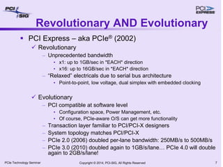
Copyright © 2014, PCI-SIG, All Rights Reserved 1
PCI Express® Basics &
Background
Richard Solomon
Synopsys
PCIe Technology Seminar 2
Acknowledgements
Thanks are due to Ravi Budruk,
Mindshare, Inc. for much of the
material on PCI Express Basics
2
Copyright © 2014, PCI-SIG, All Rights Reserved
PCIe Technology Seminar
Agenda
 PCI Express Background
 PCI Express Basics
 PCI Express Recent Developments
Copyright © 2014, PCI-SIG, All Rights Reserved 3
PCIe Technology Seminar 4
PCI Express Background
Copyright © 2014, PCI-SIG, All Rights Reserved
PCIe Technology Seminar Copyright © 2014, PCI-SIG, All Rights Reserved 5
Revolutionary AND Evolutionary
 PCI™ (1992/1993)
 Revolutionary
– Plug and Play jumperless configuration (BARs)
– Unprecedented bandwidth
• 32-bit / 33MHz – 133MB/sec
• 64-bit / 66MHz – 533MB/sec
– Designed from day 1 for bus-mastering adapters
 Evolutionary
– System BIOS maps devices then operating systems boot and
run without further knowledge of PCI
– PCI-aware O/S could gain improved functionality
– PCI 2.1 (1995) doubled bandwidth with 66MHz mode
PCIe Technology Seminar Copyright © 2014, PCI-SIG, All Rights Reserved 6
Revolutionary AND Evolutionary
 PCI-X™ (1999)
 Revolutionary
– Unprecedented bandwidth
• Up to 1066MB/sec with 64-bit / 133MHz
– Registered bus protocol
• Eased electrical timing requirements
– Brought split transactions into PCI “world”
 Evolutionary
– PCI compatible at hardware *AND* software levels
– PCI-X 2.0 (2003) doubled bandwidth
• 2133MB/sec at PCI-X 266 and 4266MB/sec at PCI-X 533
PCIe Technology Seminar Copyright © 2014, PCI-SIG, All Rights Reserved 7
Revolutionary AND Evolutionary
 PCI Express – aka PCIe® (2002)
 Revolutionary
– Unprecedented bandwidth
• x1: up to 1GB/sec in *EACH* direction
• x16: up to 16GB/sec in *EACH* direction
– “Relaxed” electricals due to serial bus architecture
• Point-to-point, low voltage, dual simplex with embedded clocking
 Evolutionary
– PCI compatible at software level
• Configuration space, Power Management, etc.
• Of course, PCIe-aware O/S can get more functionality
– Transaction layer familiar to PCI/PCI-X designers
– System topology matches PCI/PCI-X
– PCIe 2.0 (2006) doubled per-lane bandwidth: 250MB/s to 500MB/s
– PCIe 3.0 (2010) doubled again to 1GB/s/lane… PCIe 4.0 will double
again to 2GB/s/lane!
PCIe Technology Seminar Copyright © 2014, PCI-SIG, All Rights Reserved 8
PCI Concepts
PCIe Technology Seminar Copyright © 2014, PCI-SIG, All Rights Reserved 9
Address Spaces – Memory & I/O
 Memory space mapped cleanly to CPU semantics
 32-bits of address space initially
 64-bits introduced via Dual-Address Cycles (DAC)
– Extra clock of address time on PCI/PCI-X
– 4 DWORD header in PCI Express
 Burstable
 I/O space mapped cleanly to CPU semantics
 32-bits of address space
– Actually much larger than CPUs of the time
 Non-burstable
– Most PCI implementations didn’t support
– PCI-X codified
– Carries forward to PCI Express
PCIe Technology Seminar Copyright © 2014, PCI-SIG, All Rights Reserved 10
Address Spaces – Configuration
 Configuration space???
 Allows control of devices’ address decodes without conflict
 No conceptual mapping to CPU address space
– Memory-based access mechanisms in PCI-X and PCIe
 Bus / Device / Function (aka BDF) form hierarchy-based address
(PCIe 3.0 calls this “Routing ID”)
– “Functions” allow multiple, logically independent agents in one
physical device
• E.g. combination SCSI + Ethernet device
• 256 bytes or 4K bytes of configuration space per device
– PCI/PCI-X bridges form hierarchy
– PCIe switches form hierarchy
• Look like PCI-PCI bridges to software
 “Type 0” and “Type 1” configuration cycles
– Type 0: to same bus segment
– Type 1: to another bus segment
PCIe Technology Seminar Copyright © 2014, PCI-SIG, All Rights Reserved 11
Configuration Space (cont’d)
Processor Processor
Processor
Processor
Host/PCI Bridge
Bus = 0
Subord = 3
Host/PCI Bridge
Bus = 4
Subord = 5
Main
Memory
PCI Bus 0
PCI Bus 1
PCI Bus 2
PCI Bus 4
PCI Bus 5
PCI-to-PCI
Bridge
Primary = 0
Secondary = 1
Subord = 3
PCI-to-PCI
Bridge
Primary = 4
Secondary = 5
Subord = 5
PCI-to-PCI
Bridge
Primary = 1
Secondary = 2
Subord = 2
PCI Bus 3
PCI-to-PCI
Bridge
Primary = 1
Secondary = 3
Subord = 3
Address Port Data Port Address Port Data Port
PCIe Technology Seminar Copyright © 2014, PCI-SIG, All Rights Reserved 12
Configuration Space
 Device Identification
 VendorID: PCI-SIG assigned
 DeviceID: Vendor self-assigned
 Subsystem VendorID: PCI-SIG
 Subsystem DeviceID: Vendor
 Address Decode controls
 Software reads/writes BARs to
determine required size and maps
appropriately
 Memory, I/O, and bus-master
enables
 Other bus-oriented controls
PCIe Technology Seminar Copyright © 2014, PCI-SIG, All Rights Reserved 13
Configuration Space –
Capabilities List
 Linked list
 Follow the list! Cannot assume fixed location of any
given feature in any given device
 Features defined in their related specs:
– PCI-X
– PCIe
– PCI Power Management
– Etc.
Capability ID
Pointer to
Next Capability
Feature-specific
Configuration Registers
0
7
8
15
31 16
Dword n
Dword 1
Dword 0
PCIe Technology Seminar Copyright © 2014, PCI-SIG, All Rights Reserved 14
Configuration Space –
Extended Capabilities List
 PCI Express only
 Linked list
 Follow the list! Cannot assume fixed location of any
given feature in any given device
 First entry in list is *always* at 100h
 Features defined in PCI Express specification
Capability ID
Pointer to Next
Capability
Feature-specific Configuration Registers
0
7
8
15
31 16
Dword n
Dword 1
Dword 0
19
20
Version
PCIe Technology Seminar Copyright © 2014, PCI-SIG, All Rights Reserved 15
Interrupts
 PCI introduced INTA#, INTB#, INTC#, INTD# -
collectively referred to as INTx
 Level sensitive
 Decoupled device from CPU interrupt
 System controlled INTx to CPU interrupt mapping
 Configuration registers
– report A/B/C/D
– programmed with CPU interrupt number
 PCI Express mimics this via “virtual wire”
messages
 Assert_INTx and Deassert_INTx
PCIe Technology Seminar Copyright © 2014, PCI-SIG, All Rights Reserved 16
What are MSI and MSI-X?
 Memory Write replaces previous interrupt
semantics
 PCI and PCI-X devices stop asserting INTA/B/C/D
and PCI Express devices stop sending Assert_INTx
messages once MSI or MSI-X mode is enabled
 MSI uses one address with a variable data value
indicating which “vector” is asserting
 MSI-X uses a table of independent address and data
pairs for each “vector”
 NOTE: Boot devices and any device intended for
a non-MSI operating system generally must still
support the appropriate INTx signaling!
PCIe Technology Seminar Copyright © 2014, PCI-SIG, All Rights Reserved 17
Split Transactions – Background
 PCI commands contained no length
 Bus allowed disconnects and retries
 Difficult data management for target device
– Writes overflow buffers
– Reads require pre-fetch
• How much to pre-fetch? When to discard? Prevent stale data?
 PCI commands contained no initiator information
 No way for target device to begin communication with
the initiator
 Peer-to-peer requires knowledge of system-assigned
addresses
PCIe Technology Seminar Copyright © 2014, PCI-SIG, All Rights Reserved 18
Split Transactions
 PCI-X commands added length and Routing ID
of initiator
 Writes: allow target device to allocate buffers
 Reads: Pre-fetch now deterministic
 PCI-X retains “retry” & “disconnect”, adds “split”
 Telephone analogy
 Retry: “I’m busy go away”
– Delayed transactions are complicated
 Split: “I’ll call you back”
– Simple
– More efficient
PCIe Technology Seminar Copyright © 2014, PCI-SIG, All Rights Reserved 19
Benefits of Split Transactions
25
50
100
125
150
175
200
225
250
275
Number of Load Exerciser Cards
1 2 3 4 5
Bandwidth
MegaBytes/sec
50%
60%
70%
80%
90%
100%
10%
20%
30%
40%
Percent
of
Total
Bandwidth
25
50
100
125
150
175
200
225
250
275
Number of Load Exerciser Cards
2
1
50%
60%
70%
80%
90%
100%
10%
20%
30%
40%
Percent
of
Total
BandWidth
System Overhead
-- Scheduling
Transaction Overhead
-- Addressing and Routing
Transaction Data Payload
-- Actual user data
Idle Time
-- Unused BW
Transaction
Data Payload
-- Actual user
data
Idle Time
-- Unused BW
System Overhead
-- Scheduling
Transaction Overhead
-- Addressing and Routing
Bandwidth
MegaBytes/sec
Bandwidth Usage with
Conventional PCI Protocols
Bandwidth Usage with
PCI-X Enhancements
PCIe Technology Seminar Copyright © 2014, PCI-SIG, All Rights Reserved 20
PCI Express Basics
PCIe Technology Seminar Copyright © 2014, PCI-SIG, All Rights Reserved 21
PCI Express Features
 Dual Simplex point-to-point serial connection
 Independent transmit and receive sides
 Scalable Link Widths
 x1, x2, x4, x8, x12, x16, x32
 Scalable Link Speeds
 2.5, 5.0 and 8.0GT/s (16GT/s coming in 4.0)
 Packet based transaction protocol
PCIe
Device
A
PCIe
Device
B
Link (x1, x2, x4, x8, x12, x16 or x32)
Packet
Packet
PCIe Technology Seminar Copyright © 2014, PCI-SIG, All Rights Reserved 22
Link
Lane
PCI Express Terminology
PCI Express Device A
PCI Express Device B
Signal
Wire
PCIe Technology Seminar Copyright © 2014, PCI-SIG, All Rights Reserved 23
PCI Express Throughput
Derivation of these numbers:
 20% overhead due to 8b/10b encoding in 1.x and 2.x
 Note: ~1.5% overhead due to 128/130 encoding not
reflected above in 3.x and 4.0
Bandwidth (GB/s)
Link Width
x1 x2 x4 x8 x16
PCIe 1.x
“2.5 GT/s”
0.25 0.5 1 2 4
PCIe 2.x
“5 GT/s”
0.5 1 2 4 8
PCIe 3.0
“8 GT/s”
1 2 4 8 16
PCIe 4.0
“16GT/s”
2 4 8 16 32
PCIe Technology Seminar Copyright © 2014, PCI-SIG, All Rights Reserved 24
Additional Features
 Data Integrity and Error Handling
 Link-level “LCRC”
 Link-level “ACK/NAK”
 End-to-end “ECRC”
 Credit-based Flow Control
 No retry as in PCI
 MSI/MSI-X style interrupt handling
 Also supports legacy PCI interrupt handling in-band
 Advanced power management
 Active State PM
 PCI compatible PM
PCIe Technology Seminar Copyright © 2014, PCI-SIG, All Rights Reserved 25
Additional Features
 Evolutionary PCI-compatible software model
 PCI configuration and enumeration software can
be used to enumerate PCI Express hardware
 PCI Express system will boot “PCI” OS
 PCI Express supports “PCI” device drivers
 New additional configuration address space
requires OS and driver update
– Advanced Error Reporting (AER)
– PCI Express Link Controls
PCIe Technology Seminar Copyright © 2014, PCI-SIG, All Rights Reserved 26
PCI Express Topology
Switch
PCIe
Endpoint
Legacy
Endpoint
PCIe
Endpoint
Root Complex
CPU
PCIe 1
Memory
PCIe
Bridge To
PCIe 6 PCIe 7
PCIe 4 PCIe 5
Legend
PCI Express Device Downstream Port
PCI Express Device Upstream Port
PCIe
Endpoint
Switch
Virtual
PCI
Bridge
Virtual
PCI
Bridge
Virtual
PCI
Bridge
Virtual
PCI
Bridge
PCI/PCI-X
PCI/PCI-X
Bus 2
PCIe 3
Bus 8
Bus 0 (Internal)
PCIe Technology Seminar Copyright © 2014, PCI-SIG, All Rights Reserved 27
 Request are translated to one of four transaction types by
the Transaction Layer:
1. Memory Read or Memory Write. Used to transfer data from or to a
memory mapped location.
– The protocol also supports a locked memory read transaction variant
2. I/O Read or I/O Write. Used to transfer data from or to an I/O location.
– These transactions are restricted to supporting legacy endpoint
devices
3. Configuration Read or Configuration Write. Used to discover device
capabilities, program features, and check status in the 4KB PCI Express
configuration space.
4. Messages. Handled like posted writes. Used for event signaling and
general purpose messaging.
Transaction Types,
Address Spaces
PCIe Technology Seminar Copyright © 2014, PCI-SIG, All Rights Reserved 28
 Each request or completion header is tagged as to its type, and
each of the packet types is routed based on one of three
schemes:
 Address Routing
 ID Routing
 Implicit Routing
 Memory and IO requests use address routing
 Completions and Configuration cycles use ID routing
 Message requests have selectable routing based on a 3-bit
code in the message routing sub-field of the header type field
Three Methods For Packet
Routing
PCIe Technology Seminar Copyright © 2014, PCI-SIG, All Rights Reserved 29
Programmed I/O Transaction
Processor Processor
Root Complex
DDR
SDRAM
Endpoint Endpoint Endpoint
Endpoint Endpoint
Switch A Switch C
Switch B
FSB
MRd
MRd
MRd CplD
CplD
CplD
Requester:
-Step 1: Root Complex (requester)
initiates Memory Read Request (MRd)
-Step 4: Root Complex receives CplD
Completer:
-Step 2: Endpoint (completer)
receives MRd
-Step 3: Endpoint returns
Completion with data (CplD)
MRd
PCIe Technology Seminar Copyright © 2014, PCI-SIG, All Rights Reserved 30
Processor Processor
Root Complex
DDR
SDRAM
Endpoint Endpoint Endpoint
Endpoint
Switch A Switch C
Switch B
FSB
Requester:
-Step 1: Endpoint (requester)
initiates Memory Read Request (MRd)
-Step 4: Endpoint receives CplD
MRd
MRd
MRd
Completer:
-Step 2: Root Complex (completer)
receives MRd
-Step 3: Root Complex returns
Completion with data (CplD)
CplD
CplD
CplD
Endpoint
DMA Transaction
PCIe Technology Seminar Copyright © 2014, PCI-SIG, All Rights Reserved 31
Processor Processor
Root Complex
DDR
SDRAM
Endpoint Endpoint Endpoint
Endpoint Endpoint
Switch A Switch C
Switch B
FSB
Requester:
-Step 1: Endpoint (requester)
initiates Memory Read Request (MRd)
-Step 4: Endpoint receives CplD
MRd
MRd
MRd
Completer:
-Step 2: Endpoint (completer)
receives MRd
-Step 3: Endpoint returns
Completion with data (CplD)
CplD
CplD
CplD MRd
MRd CplD
CplD
Peer-to-Peer Transaction
PCIe Technology Seminar Copyright © 2014, PCI-SIG, All Rights Reserved 32
Device Core
PCI Express Core
Logic Interface
Transaction Layer
Data Link Layer
Physical Layer
TX RX
PCI Express Device A
Device Core
PCI Express Core
Logic Interface
Transaction Layer
Data Link Layer
Physical Layer
TX RX
PCI Express Device B
Link
TLP
Transmitted
TLP
Received
TLP Origin and Destination
PCIe Technology Seminar Copyright © 2014, PCI-SIG, All Rights Reserved 33
Created by Transaction Layer
Appended by Data Link Layer
Appended by Physical Layer
Bit transmit direction
Information in core section of TLP comes
from Software Layer / Device Core
TLP Structure
Header Data Payload ECRC
Sequence LCRC
Start End
1B 2B 1DW 1B
1DW
0-1024 DW
3-4 DW
PCIe Technology Seminar Copyright © 2014, PCI-SIG, All Rights Reserved 34
Device Core
PCI Express Core
Logic Interface
Transaction Layer
Data Link Layer
Physical Layer
TX RX
PCI Express Device A
Device Core
PCI Express Core
Logic Interface
Transaction Layer
Data Link Layer
Physical Layer
TX RX
PCI Express Device B
Link
DLLP
Transmitted
DLLP
Received
DLLP Origin and Destination
PCIe Technology Seminar Copyright © 2014, PCI-SIG, All Rights Reserved 35
Start End
DLLP CRC
Data Link Layer
Appended by Physical Layer
Bit transmit direction
DLLP Structure
 ACK / NAK Packets
 Flow Control Packets
 Power Management Packets
 Vendor Defined Packets
1B 4B 2B 1B
PCIe Technology Seminar Copyright © 2014, PCI-SIG, All Rights Reserved 36
Device Core
PCI Express Core
Logic Interface
Transaction Layer
Data Link Layer
Physical Layer
TX RX
PCI Express Device A
Device Core
PCI Express Core
Logic Interface
Transaction Layer
Data Link Layer
Physical Layer
TX RX
PCI Express Device B
Link
Ordered-Set
Transmitted
Ordered-Set
Received
Ordered-Set Origin and
Destination
PCIe Technology Seminar Copyright © 2014, PCI-SIG, All Rights Reserved 37
COM Identifier Identifier Identifier
 Training Sequence One (TS1)
 16 character set: 1 COM, 15 TS1 data characters
 Training Sequence Two (TS2)
 16 character set: 1 COM, 15 TS2 data characters
 SKIP
 4 character set: 1 COM followed by 3 SKP identifiers
 Fast Training Sequence (FTS)
 4 characters: 1 COM followed by 3 FTS identifiers
 Electrical Idle (IDLE)
 4 characters: 1 COM followed by 3 IDL identifiers
 Electrical Idle Exit (EIEOS) (new to 2.0 spec)
 16 characters
Ordered-Set Structure
PCIe Technology Seminar Copyright © 2014, PCI-SIG, All Rights Reserved 38
 Credit-based flow control is point-to-point
based, not end-to-end
Receiver
Transmitter
Flow Control DLLP (FCx)
TLP
VC Buffer
Receiver sends Flow Control Packets (FCP) which are a type of DLLP (Data Link Layer Packet)
to provide the transmitter with credits so that it can transmit packets to the receiver
Buffer space
available
PCI Express Flow Control
PCIe Technology Seminar Copyright © 2014, PCI-SIG, All Rights Reserved 39
Replay
Buffer
ACK /
NAK
DLLP
De-mux
Mux
From
Transaction Layer
Data Link Layer
Tx Rx
TLP
Sequence TLP LCRC
Transmit
Device A
Receiver
Device B
Tx
Error
Check
TLP
Sequence TLP LCRC
De-mux
Mux
To
Transaction Layer
Data Link Layer
Tx Rx
ACK /
NAK
DLLP
Rx
TLP
Sequence TLP LCRC
ACK /
NAK
DLLP
Link
ACK/NAK Protocol Overview
PCIe Technology Seminar Copyright © 2014, PCI-SIG, All Rights Reserved 40
PCI Express
Recent Developments
PCIe Technology Seminar
New Specifications
 M.2 Specification, Revision 1.0
https://www.pcisig.com/members/downloads/PCIe_M.2_Electromechanical_Sp
ec_Rev1.0_Final_11012013_RS_Clean.pdf
 PCI Express Base 4.0, Draft 0.3
https://www.pcisig.com/members/downloads/PCI_Express_Base_4.0_Rev0.3_
February19-2014.pdf
 OCuLink, Draft 0.7
https://www.pcisig.com/members/downloads/OCuLink_07_r11_1010a.pdf
 SFF-8639, Draft 0.7
https://www.pcisig.com/members/downloads/PCIe_SFF_03312014TS-rev1-
markup.pdf
Copyright © 2014, PCI-SIG, All Rights Reserved 41
PCIe Technology Seminar
Newer ECNs
(See session 4 after lunch for details)
 NOP DLLP
https://www.pcisig.com/specifications/pciexpress/specifications/ECN_NOP_DL
LP-2014-06-11_clean.pdf
 Readiness Notifications (RN)
https://www.pcisig.com/specifications/pciexpress/specifications/ECN_RN_29_A
ug_2013.pdf
 M-PCIe
https://www.pcisig.com/specifications/pciexpress/specifications/ECN_M-
PCIe_22_May_2013.pdf
 L1 PM Substates
https://www.pcisig.com/specifications/pciexpress/specifications/ECN_L1_PM_S
ubstates_with_CLKREQ_31_May_2013_Rev10a.pdf
Copyright © 2014, PCI-SIG, All Rights Reserved 42
PCIe Technology Seminar
Upcoming Events
 Compliance Workshop #91 (Taipei)
 Tomorrow 
 Compliance Workshop #92 (California)
 December 2-5, 2014
 PCI-SIG Developers Conference Israel
 March 2-3, 2015
 PCI-SIG Developers Conference
 June 23-24, 2015
 PCI-SIG Developers Conference APAC
 [TBD] October 2015?
Copyright © 2014, PCI-SIG, All Rights Reserved 43
PCIe Technology Seminar Copyright © 2014, PCI-SIG, All Rights Reserved 44
Present a DevCon Member
Implementation Session
 Watch for e-mailed Call For Papers
 Send in an abstract!
 160 word summary
– Ok to attach more detail (even a presentation)
 No confidential material!
 Not a datasheet or catalog or other marketing!
 Get selected
 Meet milestones and deadlines
 Practice, practice, practice the presentation
 Present at DevCon
PCIe Technology Seminar Copyright © 2014, PCI-SIG, All Rights Reserved 45
Thank you for attending the
PCIe Technology Seminar.
For more information please go to
www.pcisig.com

PCI_Express_Basics_Background.pdf

  • 1.
    Copyright © 2014,PCI-SIG, All Rights Reserved 1 PCI Express® Basics & Background Richard Solomon Synopsys
  • 2.
    PCIe Technology Seminar2 Acknowledgements Thanks are due to Ravi Budruk, Mindshare, Inc. for much of the material on PCI Express Basics 2 Copyright © 2014, PCI-SIG, All Rights Reserved
  • 3.
    PCIe Technology Seminar Agenda PCI Express Background  PCI Express Basics  PCI Express Recent Developments Copyright © 2014, PCI-SIG, All Rights Reserved 3
  • 4.
    PCIe Technology Seminar4 PCI Express Background Copyright © 2014, PCI-SIG, All Rights Reserved
  • 5.
    PCIe Technology SeminarCopyright © 2014, PCI-SIG, All Rights Reserved 5 Revolutionary AND Evolutionary  PCI™ (1992/1993)  Revolutionary – Plug and Play jumperless configuration (BARs) – Unprecedented bandwidth • 32-bit / 33MHz – 133MB/sec • 64-bit / 66MHz – 533MB/sec – Designed from day 1 for bus-mastering adapters  Evolutionary – System BIOS maps devices then operating systems boot and run without further knowledge of PCI – PCI-aware O/S could gain improved functionality – PCI 2.1 (1995) doubled bandwidth with 66MHz mode
  • 6.
    PCIe Technology SeminarCopyright © 2014, PCI-SIG, All Rights Reserved 6 Revolutionary AND Evolutionary  PCI-X™ (1999)  Revolutionary – Unprecedented bandwidth • Up to 1066MB/sec with 64-bit / 133MHz – Registered bus protocol • Eased electrical timing requirements – Brought split transactions into PCI “world”  Evolutionary – PCI compatible at hardware *AND* software levels – PCI-X 2.0 (2003) doubled bandwidth • 2133MB/sec at PCI-X 266 and 4266MB/sec at PCI-X 533
  • 7.
    PCIe Technology SeminarCopyright © 2014, PCI-SIG, All Rights Reserved 7 Revolutionary AND Evolutionary  PCI Express – aka PCIe® (2002)  Revolutionary – Unprecedented bandwidth • x1: up to 1GB/sec in *EACH* direction • x16: up to 16GB/sec in *EACH* direction – “Relaxed” electricals due to serial bus architecture • Point-to-point, low voltage, dual simplex with embedded clocking  Evolutionary – PCI compatible at software level • Configuration space, Power Management, etc. • Of course, PCIe-aware O/S can get more functionality – Transaction layer familiar to PCI/PCI-X designers – System topology matches PCI/PCI-X – PCIe 2.0 (2006) doubled per-lane bandwidth: 250MB/s to 500MB/s – PCIe 3.0 (2010) doubled again to 1GB/s/lane… PCIe 4.0 will double again to 2GB/s/lane!
  • 8.
    PCIe Technology SeminarCopyright © 2014, PCI-SIG, All Rights Reserved 8 PCI Concepts
  • 9.
    PCIe Technology SeminarCopyright © 2014, PCI-SIG, All Rights Reserved 9 Address Spaces – Memory & I/O  Memory space mapped cleanly to CPU semantics  32-bits of address space initially  64-bits introduced via Dual-Address Cycles (DAC) – Extra clock of address time on PCI/PCI-X – 4 DWORD header in PCI Express  Burstable  I/O space mapped cleanly to CPU semantics  32-bits of address space – Actually much larger than CPUs of the time  Non-burstable – Most PCI implementations didn’t support – PCI-X codified – Carries forward to PCI Express
  • 10.
    PCIe Technology SeminarCopyright © 2014, PCI-SIG, All Rights Reserved 10 Address Spaces – Configuration  Configuration space???  Allows control of devices’ address decodes without conflict  No conceptual mapping to CPU address space – Memory-based access mechanisms in PCI-X and PCIe  Bus / Device / Function (aka BDF) form hierarchy-based address (PCIe 3.0 calls this “Routing ID”) – “Functions” allow multiple, logically independent agents in one physical device • E.g. combination SCSI + Ethernet device • 256 bytes or 4K bytes of configuration space per device – PCI/PCI-X bridges form hierarchy – PCIe switches form hierarchy • Look like PCI-PCI bridges to software  “Type 0” and “Type 1” configuration cycles – Type 0: to same bus segment – Type 1: to another bus segment
  • 11.
    PCIe Technology SeminarCopyright © 2014, PCI-SIG, All Rights Reserved 11 Configuration Space (cont’d) Processor Processor Processor Processor Host/PCI Bridge Bus = 0 Subord = 3 Host/PCI Bridge Bus = 4 Subord = 5 Main Memory PCI Bus 0 PCI Bus 1 PCI Bus 2 PCI Bus 4 PCI Bus 5 PCI-to-PCI Bridge Primary = 0 Secondary = 1 Subord = 3 PCI-to-PCI Bridge Primary = 4 Secondary = 5 Subord = 5 PCI-to-PCI Bridge Primary = 1 Secondary = 2 Subord = 2 PCI Bus 3 PCI-to-PCI Bridge Primary = 1 Secondary = 3 Subord = 3 Address Port Data Port Address Port Data Port
  • 12.
    PCIe Technology SeminarCopyright © 2014, PCI-SIG, All Rights Reserved 12 Configuration Space  Device Identification  VendorID: PCI-SIG assigned  DeviceID: Vendor self-assigned  Subsystem VendorID: PCI-SIG  Subsystem DeviceID: Vendor  Address Decode controls  Software reads/writes BARs to determine required size and maps appropriately  Memory, I/O, and bus-master enables  Other bus-oriented controls
  • 13.
    PCIe Technology SeminarCopyright © 2014, PCI-SIG, All Rights Reserved 13 Configuration Space – Capabilities List  Linked list  Follow the list! Cannot assume fixed location of any given feature in any given device  Features defined in their related specs: – PCI-X – PCIe – PCI Power Management – Etc. Capability ID Pointer to Next Capability Feature-specific Configuration Registers 0 7 8 15 31 16 Dword n Dword 1 Dword 0
  • 14.
    PCIe Technology SeminarCopyright © 2014, PCI-SIG, All Rights Reserved 14 Configuration Space – Extended Capabilities List  PCI Express only  Linked list  Follow the list! Cannot assume fixed location of any given feature in any given device  First entry in list is *always* at 100h  Features defined in PCI Express specification Capability ID Pointer to Next Capability Feature-specific Configuration Registers 0 7 8 15 31 16 Dword n Dword 1 Dword 0 19 20 Version
  • 15.
    PCIe Technology SeminarCopyright © 2014, PCI-SIG, All Rights Reserved 15 Interrupts  PCI introduced INTA#, INTB#, INTC#, INTD# - collectively referred to as INTx  Level sensitive  Decoupled device from CPU interrupt  System controlled INTx to CPU interrupt mapping  Configuration registers – report A/B/C/D – programmed with CPU interrupt number  PCI Express mimics this via “virtual wire” messages  Assert_INTx and Deassert_INTx
  • 16.
    PCIe Technology SeminarCopyright © 2014, PCI-SIG, All Rights Reserved 16 What are MSI and MSI-X?  Memory Write replaces previous interrupt semantics  PCI and PCI-X devices stop asserting INTA/B/C/D and PCI Express devices stop sending Assert_INTx messages once MSI or MSI-X mode is enabled  MSI uses one address with a variable data value indicating which “vector” is asserting  MSI-X uses a table of independent address and data pairs for each “vector”  NOTE: Boot devices and any device intended for a non-MSI operating system generally must still support the appropriate INTx signaling!
  • 17.
    PCIe Technology SeminarCopyright © 2014, PCI-SIG, All Rights Reserved 17 Split Transactions – Background  PCI commands contained no length  Bus allowed disconnects and retries  Difficult data management for target device – Writes overflow buffers – Reads require pre-fetch • How much to pre-fetch? When to discard? Prevent stale data?  PCI commands contained no initiator information  No way for target device to begin communication with the initiator  Peer-to-peer requires knowledge of system-assigned addresses
  • 18.
    PCIe Technology SeminarCopyright © 2014, PCI-SIG, All Rights Reserved 18 Split Transactions  PCI-X commands added length and Routing ID of initiator  Writes: allow target device to allocate buffers  Reads: Pre-fetch now deterministic  PCI-X retains “retry” & “disconnect”, adds “split”  Telephone analogy  Retry: “I’m busy go away” – Delayed transactions are complicated  Split: “I’ll call you back” – Simple – More efficient
  • 19.
    PCIe Technology SeminarCopyright © 2014, PCI-SIG, All Rights Reserved 19 Benefits of Split Transactions 25 50 100 125 150 175 200 225 250 275 Number of Load Exerciser Cards 1 2 3 4 5 Bandwidth MegaBytes/sec 50% 60% 70% 80% 90% 100% 10% 20% 30% 40% Percent of Total Bandwidth 25 50 100 125 150 175 200 225 250 275 Number of Load Exerciser Cards 2 1 50% 60% 70% 80% 90% 100% 10% 20% 30% 40% Percent of Total BandWidth System Overhead -- Scheduling Transaction Overhead -- Addressing and Routing Transaction Data Payload -- Actual user data Idle Time -- Unused BW Transaction Data Payload -- Actual user data Idle Time -- Unused BW System Overhead -- Scheduling Transaction Overhead -- Addressing and Routing Bandwidth MegaBytes/sec Bandwidth Usage with Conventional PCI Protocols Bandwidth Usage with PCI-X Enhancements
  • 20.
    PCIe Technology SeminarCopyright © 2014, PCI-SIG, All Rights Reserved 20 PCI Express Basics
  • 21.
    PCIe Technology SeminarCopyright © 2014, PCI-SIG, All Rights Reserved 21 PCI Express Features  Dual Simplex point-to-point serial connection  Independent transmit and receive sides  Scalable Link Widths  x1, x2, x4, x8, x12, x16, x32  Scalable Link Speeds  2.5, 5.0 and 8.0GT/s (16GT/s coming in 4.0)  Packet based transaction protocol PCIe Device A PCIe Device B Link (x1, x2, x4, x8, x12, x16 or x32) Packet Packet
  • 22.
    PCIe Technology SeminarCopyright © 2014, PCI-SIG, All Rights Reserved 22 Link Lane PCI Express Terminology PCI Express Device A PCI Express Device B Signal Wire
  • 23.
    PCIe Technology SeminarCopyright © 2014, PCI-SIG, All Rights Reserved 23 PCI Express Throughput Derivation of these numbers:  20% overhead due to 8b/10b encoding in 1.x and 2.x  Note: ~1.5% overhead due to 128/130 encoding not reflected above in 3.x and 4.0 Bandwidth (GB/s) Link Width x1 x2 x4 x8 x16 PCIe 1.x “2.5 GT/s” 0.25 0.5 1 2 4 PCIe 2.x “5 GT/s” 0.5 1 2 4 8 PCIe 3.0 “8 GT/s” 1 2 4 8 16 PCIe 4.0 “16GT/s” 2 4 8 16 32
  • 24.
    PCIe Technology SeminarCopyright © 2014, PCI-SIG, All Rights Reserved 24 Additional Features  Data Integrity and Error Handling  Link-level “LCRC”  Link-level “ACK/NAK”  End-to-end “ECRC”  Credit-based Flow Control  No retry as in PCI  MSI/MSI-X style interrupt handling  Also supports legacy PCI interrupt handling in-band  Advanced power management  Active State PM  PCI compatible PM
  • 25.
    PCIe Technology SeminarCopyright © 2014, PCI-SIG, All Rights Reserved 25 Additional Features  Evolutionary PCI-compatible software model  PCI configuration and enumeration software can be used to enumerate PCI Express hardware  PCI Express system will boot “PCI” OS  PCI Express supports “PCI” device drivers  New additional configuration address space requires OS and driver update – Advanced Error Reporting (AER) – PCI Express Link Controls
  • 26.
    PCIe Technology SeminarCopyright © 2014, PCI-SIG, All Rights Reserved 26 PCI Express Topology Switch PCIe Endpoint Legacy Endpoint PCIe Endpoint Root Complex CPU PCIe 1 Memory PCIe Bridge To PCIe 6 PCIe 7 PCIe 4 PCIe 5 Legend PCI Express Device Downstream Port PCI Express Device Upstream Port PCIe Endpoint Switch Virtual PCI Bridge Virtual PCI Bridge Virtual PCI Bridge Virtual PCI Bridge PCI/PCI-X PCI/PCI-X Bus 2 PCIe 3 Bus 8 Bus 0 (Internal)
  • 27.
    PCIe Technology SeminarCopyright © 2014, PCI-SIG, All Rights Reserved 27  Request are translated to one of four transaction types by the Transaction Layer: 1. Memory Read or Memory Write. Used to transfer data from or to a memory mapped location. – The protocol also supports a locked memory read transaction variant 2. I/O Read or I/O Write. Used to transfer data from or to an I/O location. – These transactions are restricted to supporting legacy endpoint devices 3. Configuration Read or Configuration Write. Used to discover device capabilities, program features, and check status in the 4KB PCI Express configuration space. 4. Messages. Handled like posted writes. Used for event signaling and general purpose messaging. Transaction Types, Address Spaces
  • 28.
    PCIe Technology SeminarCopyright © 2014, PCI-SIG, All Rights Reserved 28  Each request or completion header is tagged as to its type, and each of the packet types is routed based on one of three schemes:  Address Routing  ID Routing  Implicit Routing  Memory and IO requests use address routing  Completions and Configuration cycles use ID routing  Message requests have selectable routing based on a 3-bit code in the message routing sub-field of the header type field Three Methods For Packet Routing
  • 29.
    PCIe Technology SeminarCopyright © 2014, PCI-SIG, All Rights Reserved 29 Programmed I/O Transaction Processor Processor Root Complex DDR SDRAM Endpoint Endpoint Endpoint Endpoint Endpoint Switch A Switch C Switch B FSB MRd MRd MRd CplD CplD CplD Requester: -Step 1: Root Complex (requester) initiates Memory Read Request (MRd) -Step 4: Root Complex receives CplD Completer: -Step 2: Endpoint (completer) receives MRd -Step 3: Endpoint returns Completion with data (CplD) MRd
  • 30.
    PCIe Technology SeminarCopyright © 2014, PCI-SIG, All Rights Reserved 30 Processor Processor Root Complex DDR SDRAM Endpoint Endpoint Endpoint Endpoint Switch A Switch C Switch B FSB Requester: -Step 1: Endpoint (requester) initiates Memory Read Request (MRd) -Step 4: Endpoint receives CplD MRd MRd MRd Completer: -Step 2: Root Complex (completer) receives MRd -Step 3: Root Complex returns Completion with data (CplD) CplD CplD CplD Endpoint DMA Transaction
  • 31.
    PCIe Technology SeminarCopyright © 2014, PCI-SIG, All Rights Reserved 31 Processor Processor Root Complex DDR SDRAM Endpoint Endpoint Endpoint Endpoint Endpoint Switch A Switch C Switch B FSB Requester: -Step 1: Endpoint (requester) initiates Memory Read Request (MRd) -Step 4: Endpoint receives CplD MRd MRd MRd Completer: -Step 2: Endpoint (completer) receives MRd -Step 3: Endpoint returns Completion with data (CplD) CplD CplD CplD MRd MRd CplD CplD Peer-to-Peer Transaction
  • 32.
    PCIe Technology SeminarCopyright © 2014, PCI-SIG, All Rights Reserved 32 Device Core PCI Express Core Logic Interface Transaction Layer Data Link Layer Physical Layer TX RX PCI Express Device A Device Core PCI Express Core Logic Interface Transaction Layer Data Link Layer Physical Layer TX RX PCI Express Device B Link TLP Transmitted TLP Received TLP Origin and Destination
  • 33.
    PCIe Technology SeminarCopyright © 2014, PCI-SIG, All Rights Reserved 33 Created by Transaction Layer Appended by Data Link Layer Appended by Physical Layer Bit transmit direction Information in core section of TLP comes from Software Layer / Device Core TLP Structure Header Data Payload ECRC Sequence LCRC Start End 1B 2B 1DW 1B 1DW 0-1024 DW 3-4 DW
  • 34.
    PCIe Technology SeminarCopyright © 2014, PCI-SIG, All Rights Reserved 34 Device Core PCI Express Core Logic Interface Transaction Layer Data Link Layer Physical Layer TX RX PCI Express Device A Device Core PCI Express Core Logic Interface Transaction Layer Data Link Layer Physical Layer TX RX PCI Express Device B Link DLLP Transmitted DLLP Received DLLP Origin and Destination
  • 35.
    PCIe Technology SeminarCopyright © 2014, PCI-SIG, All Rights Reserved 35 Start End DLLP CRC Data Link Layer Appended by Physical Layer Bit transmit direction DLLP Structure  ACK / NAK Packets  Flow Control Packets  Power Management Packets  Vendor Defined Packets 1B 4B 2B 1B
  • 36.
    PCIe Technology SeminarCopyright © 2014, PCI-SIG, All Rights Reserved 36 Device Core PCI Express Core Logic Interface Transaction Layer Data Link Layer Physical Layer TX RX PCI Express Device A Device Core PCI Express Core Logic Interface Transaction Layer Data Link Layer Physical Layer TX RX PCI Express Device B Link Ordered-Set Transmitted Ordered-Set Received Ordered-Set Origin and Destination
  • 37.
    PCIe Technology SeminarCopyright © 2014, PCI-SIG, All Rights Reserved 37 COM Identifier Identifier Identifier  Training Sequence One (TS1)  16 character set: 1 COM, 15 TS1 data characters  Training Sequence Two (TS2)  16 character set: 1 COM, 15 TS2 data characters  SKIP  4 character set: 1 COM followed by 3 SKP identifiers  Fast Training Sequence (FTS)  4 characters: 1 COM followed by 3 FTS identifiers  Electrical Idle (IDLE)  4 characters: 1 COM followed by 3 IDL identifiers  Electrical Idle Exit (EIEOS) (new to 2.0 spec)  16 characters Ordered-Set Structure
  • 38.
    PCIe Technology SeminarCopyright © 2014, PCI-SIG, All Rights Reserved 38  Credit-based flow control is point-to-point based, not end-to-end Receiver Transmitter Flow Control DLLP (FCx) TLP VC Buffer Receiver sends Flow Control Packets (FCP) which are a type of DLLP (Data Link Layer Packet) to provide the transmitter with credits so that it can transmit packets to the receiver Buffer space available PCI Express Flow Control
  • 39.
    PCIe Technology SeminarCopyright © 2014, PCI-SIG, All Rights Reserved 39 Replay Buffer ACK / NAK DLLP De-mux Mux From Transaction Layer Data Link Layer Tx Rx TLP Sequence TLP LCRC Transmit Device A Receiver Device B Tx Error Check TLP Sequence TLP LCRC De-mux Mux To Transaction Layer Data Link Layer Tx Rx ACK / NAK DLLP Rx TLP Sequence TLP LCRC ACK / NAK DLLP Link ACK/NAK Protocol Overview
  • 40.
    PCIe Technology SeminarCopyright © 2014, PCI-SIG, All Rights Reserved 40 PCI Express Recent Developments
  • 41.
    PCIe Technology Seminar NewSpecifications  M.2 Specification, Revision 1.0 https://www.pcisig.com/members/downloads/PCIe_M.2_Electromechanical_Sp ec_Rev1.0_Final_11012013_RS_Clean.pdf  PCI Express Base 4.0, Draft 0.3 https://www.pcisig.com/members/downloads/PCI_Express_Base_4.0_Rev0.3_ February19-2014.pdf  OCuLink, Draft 0.7 https://www.pcisig.com/members/downloads/OCuLink_07_r11_1010a.pdf  SFF-8639, Draft 0.7 https://www.pcisig.com/members/downloads/PCIe_SFF_03312014TS-rev1- markup.pdf Copyright © 2014, PCI-SIG, All Rights Reserved 41
  • 42.
    PCIe Technology Seminar NewerECNs (See session 4 after lunch for details)  NOP DLLP https://www.pcisig.com/specifications/pciexpress/specifications/ECN_NOP_DL LP-2014-06-11_clean.pdf  Readiness Notifications (RN) https://www.pcisig.com/specifications/pciexpress/specifications/ECN_RN_29_A ug_2013.pdf  M-PCIe https://www.pcisig.com/specifications/pciexpress/specifications/ECN_M- PCIe_22_May_2013.pdf  L1 PM Substates https://www.pcisig.com/specifications/pciexpress/specifications/ECN_L1_PM_S ubstates_with_CLKREQ_31_May_2013_Rev10a.pdf Copyright © 2014, PCI-SIG, All Rights Reserved 42
  • 43.
    PCIe Technology Seminar UpcomingEvents  Compliance Workshop #91 (Taipei)  Tomorrow   Compliance Workshop #92 (California)  December 2-5, 2014  PCI-SIG Developers Conference Israel  March 2-3, 2015  PCI-SIG Developers Conference  June 23-24, 2015  PCI-SIG Developers Conference APAC  [TBD] October 2015? Copyright © 2014, PCI-SIG, All Rights Reserved 43
  • 44.
    PCIe Technology SeminarCopyright © 2014, PCI-SIG, All Rights Reserved 44 Present a DevCon Member Implementation Session  Watch for e-mailed Call For Papers  Send in an abstract!  160 word summary – Ok to attach more detail (even a presentation)  No confidential material!  Not a datasheet or catalog or other marketing!  Get selected  Meet milestones and deadlines  Practice, practice, practice the presentation  Present at DevCon
  • 45.
    PCIe Technology SeminarCopyright © 2014, PCI-SIG, All Rights Reserved 45 Thank you for attending the PCIe Technology Seminar. For more information please go to www.pcisig.com