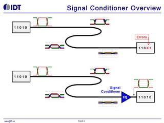
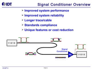
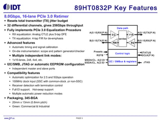
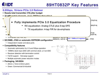
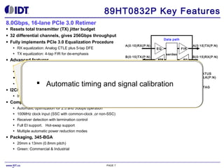
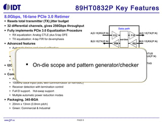
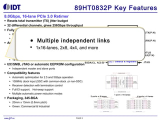
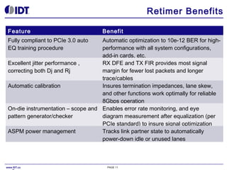
The IDT 89HT0832P is the industry's first 32-channel (16-lane) PCI Express 3.0 retimer capable of 8 Gbps-per-channel transfers, providing a total of 256 Gbps of communication bandwidth for data-intensive applications. The 89HT0832P is protocol-aware to support the PCIe 3.0-compliant equalization procedure for receiver and transmitter configuration, which eases system design-in complexity, and insures reliable low bit-error-rate (BER) operation with any PCI Express 3.0-compliant device, expansion card, or host bus adapter (HBA). The Retimer's receivers include a high-performance continuous-time linear equalizer (CTLE) analog front-end followed by a five-tap decision feedback equalizer (DFE) and clock-data-recovery (CDR) circuit. This high-performance input with dynamic optimization can recover poor quality input signals, correct random and deterministic jitter, and boost transmit amplitude -- enabling communication over long cables, long traces, or system backplanes. Presented by Ken Curt, Product manager at IDT. Learn more about IDT's signal integrity products at www.idt.com/go/SIP.
This document provides information on the features and specifications of the Atmel ATmega8(L) 8-bit microcontroller. It has an 8-bit AVR CPU with advanced RISC architecture, 8KBytes of flash memory, 512Bytes of EEPROM, 1KByte of SRAM, and various I/O features. The microcontroller operates between 2.7-5.5V with a clock speed of 0-16MHz and has low power consumption of 3.6mA active, 1.0mA idle, and 0.5uA power-down modes.
This document summarizes the features of the Atmel ATmega8L and ATmega8 microcontrollers. It includes:
- Details on the 8-bit RISC architecture, registers, speed grades up to 16MHz, and low power consumption.
- On-chip memory features including 8K flash, 512B EEPROM, and 1KB SRAM with high endurance and long data retention.
- Peripheral features such as timers, PWM, ADC, serial interfaces, and analog comparator.
- Package options, pin configurations, and operating voltages from 2.7V to 5.5V.
This document summarizes the features and specifications of an 8-bit Atmel microcontroller. It has advanced RISC architecture with powerful instructions that execute in single clock cycles. It features in-system self-programmable flash memory from 4-32KB, EEPROM from 256-1KB, and internal SRAM from 512-2KB. It has various peripheral features including timers, PWM, ADC, serial interfaces, and more. It is available in PDIP, TQFP, and other packages and operates from 1.8-5.5V over commercial and industrial temperature ranges.
This document discusses serial communication using the 8051 microcontroller. It begins by introducing serial vs parallel data transfer, communication modes, and framing. It then describes the RS-232 protocol and pinout when using the 8051 UART. Setting the baud rate using Timer 1 is explained. The document provides details on the Serial Control Register and transmitting and receiving data with the serial port. It concludes by discussing using interrupts with the serial port and providing an example of transmitting data from Port 1 and receiving to Port 0 using interrupts.
The document provides an overview of the LPC214x microcontroller family from NXP Semiconductors, which features an ARM7 processor, on-chip flash memory, RAM, analog and digital peripherals like USB, SPI, I2C, and GPIO. It describes the memory architecture and maps as well as the system control block and various peripherals included in the MCU, such as timers, serial interfaces, and an ADC. The document also outlines programming and debugging tools available for the LPC214x family like in-system programming, an embeddedICE logic for debugging, and a trace macrocell for instruction tracing.
The 8254 programmable interval timer consists of three independent 16-bit programmable counters that can each count in binary or BCD up to a maximum frequency of 10 MHz. This timer is useful for controlling real-time events in microprocessors. In personal computers, the timer generates an 18.2 Hz interrupt, refreshes DRAM memory, and provides timing to devices like speakers. Each counter has inputs and outputs to control counting. The 8254 has various modes to generate pulses, squares waves, and one-shots using the counters.
The document provides information about a microcontroller instruction set including:
- Instructions that affect flag settings and how they modify the flags.
- The instruction set and addressing modes which include registers, direct addressing, indirect addressing, constants, and branches.
- A summary of the instruction set organized in a table with the opcode, instruction name, addressing mode, and byte size/cycle information.
The document discusses various topics related to interfacing an 8051 microcontroller, including:
1. Serial communication between an 8051 and PC using RS-232 and a MAX232 chip.
2. Half-duplex and asynchronous serial communication modes.
3. Addressing modes of the 8051 including register, direct, indirect, and indexed addressing.
4. Instructions sets, registers, and programming of the 8051 microcontroller.
The document describes the Xenus XTL digital servo drive for brushless and brush motors. Some key points:
1. The Xenus drive combines CANopen networking with 100% digital control of brushless or brush motors in an off-line powered package that can operate from single or three-phase mains with continuous power output up to 4 kW.
2. It operates as a Motion Control Device under the DSP-402 protocol of the CANopen application layer and supports modes like Profile Position, Profile Velocity, Profile Torque, and Homing.
3. Drive commissioning is fast and simple using CME 2 software via CAN or RS-232 communication. Address selection is by a 16-position
The document provides an introduction to PIC18FX6J series microcontrollers from Microchip Technology, outlining their key features which include nanoWatt XLP low power technology, peripheral modules like ECCP, EUSART, MSSP, and CTMU, as well as their target applications in battery powered devices, utility metering, asset tracking, and more. It describes the core features, low power modes, clocking options, and peripheral modules in detail over 17 pages.
Analog to digital converter is one of the most important feature of micro controller. here i am explaining about basic of ADC, working and how exactly controller do it. Here i also explaining registers of ADC and attached a sample code.
This document provides an overview of microcontrollers and the 8051 microcontroller. It discusses the basic components of microprocessors and microcontrollers, compares microprocessors and microcontrollers, lists common applications of microcontrollers in embedded systems, and criteria for choosing a microcontroller. It then focuses on the features, pin descriptions and functions, and CPU operation of the 8051 microcontroller.
this ppt only for beginner who want to understand concept of Timer counter operation of LPC2148 step by step.
hope it may help u.
always welcoming ur suggestion.
The document describes an Atmel microcontroller with features such as a powerful instruction set, 32 general purpose registers, various memory segments including flash, EEPROM and SRAM, in-system programming, analog and digital peripherals, and low power consumption. It includes pinout diagrams and descriptions of the microcontroller's I/O ports, voltage supplies, and packages. Key specifications listed are operating voltage, temperature range, speed grades, and power consumption levels.
The Accelera DMC-40x0 is Galil's highest performance multi-axis motion controller, accepting encoder inputs up to 22 MHz and processing commands in as fast as 40 microseconds. It is available in 1 to 8 axis models and is configurable for stepper or servo motors. Standard features include PID control, I/O processing, and multi-axis coordinated motion capabilities like linear interpolation. The DMC-40x0 is designed for demanding motion control applications.
This document discusses analog to digital conversion and pulse width modulation.
It explains that analog signals from peripherals must be converted to digital signals the microcontroller can understand using an analog to digital converter (ADC). It also describes how pulse width modulation varies the duty cycle of a signal to control motor speed or other analog systems. Common applications like temperature measurement and motor control are provided as examples.
The document describes a lab manual for experiments with an 8085 microprocessor. It includes:
1) 13 assembly language programs to perform operations like data transfer, addition, comparison etc. using the 8085 microprocessor kit.
2) Details of the 8085 microprocessor architecture including registers, flags, pin descriptions.
3) Information about the memory map, I/O ports, and other integrated circuits used in the microprocessor kit like 8253, 8255, 8279.
4) Procedures for entering and executing programs on the microprocessor kit and expected input/output for programs.
The document provides comprehensive information needed to learn and perform various experiments on an 8085 microprocessor
The document discusses analog to digital conversion (ADC) in the LPC2148 ARM microcontroller. It notes that the LPC2148 has two 10-bit ADC modules, ADC0 and ADC1, which can convert analog signals to 10-bit digital values between 0 and 1023. It lists the main registers associated with ADC in the LPC2148, including the ADCR control register, ADGDR global data register, ADSTAT status register, and ADINTEN interrupt enable register. Finally, it provides a table showing the ADC-related channels and pins on the LPC2148.
The document discusses the 8051 microcontroller. It describes the basic components of the 8051 including 4K bytes of internal ROM, 128 bytes of internal RAM, four 8-bit I/O ports, two 16-bit timers/counters, and one serial interface. It also provides details on the block diagram, important pins like ports and serial interface pins, and how to connect an external clock source to the 8051.
The ATmega16A is a low-power CMOS 8-bit microcontroller based on the AVR enhanced RISC
architecture. By executing powerful instructions in a single clock cycle, the ATmega16A
achieves throughputs approaching 1 MIPS per MHz allowing the system designer to optimize
power consumption versus processing speed.
FP-e is an all-in-one programmable logic controller and display panel that is panel-mountable with an IP66 rating. It has basic PLC functionality equivalent to FP0-C14 models and includes a 3-color, 5-character display. Programming is easy using a wizard interface and debugging is smooth with R and I modes. Models are available with RS-232C or RS-485 communication and some include thermocouple input.
AIHRO-The Humanoid Project | Final year Btech project @ ADI SHANKARA INSTITUTE OF ENGINEERING AND TECHNOLOGY .
Project was Selected as one of the finalist in TEXAS INSTRUMENTS INNOVATION CHALLENGE 2015
The document provides an overview of the dsPIC33FJ06GSXXX digital signal controller, including its 16-bit architecture, 40 MIPS CPU speed, 6KB flash memory, 256B RAM, and peripherals such as 10-bit ADCs, PWM modules, UART, I2C, and SPI communication blocks. Application examples for the dsPIC33FJ06GSXXX include AC-DC converters, LED lighting, motor control, and power supplies. Key specifications and features of the dsPIC33FJ06GSXXX DSC are described such as its memory organization, analog and digital peripherals, and intelligent power supply applications.
The IOC-7007 is an intelligent I/O controller that can accept up to seven I/O modules to handle various input and output functions. It has an Ethernet port for communication, programmable logic for I/O control, and a programming language similar to Galil motion controllers for integration of motion and I/O. It is available as a box, DIN rail, or card level unit to accept a range of power inputs.
The Universal Asynchronous Receiver/Transmitter (UART) controller is the key component of the serial communications subsystem of a computer. The UART takes bytes of data and transmits the individual bits in a sequential fashion. At the destination, a second UART re-assembles the bits into complete bytes.
The Atmega8 microcontroller has a Harvard architecture with separate program and data memories. It features 8K of flash memory, 512 bytes of EEPROM, and 1K of SRAM. It has various digital and analog I/O ports that can be configured for input, output, and alternate functions. The Atmega8 uses an internal or external clock and has features like timers, interrupts, and PWM that make it suitable for biomedical applications.
Fcamp may2010-tech2-fpga high speed io trends-alteraTrends & Challenges in De...FPGA Central
This document discusses high-speed input/output (IO) trends, signal integrity challenges, and techniques for mitigating issues at high data rates. It begins with an overview of how serial communication protocols have increased dramatically in data rate over time. This poses new signal integrity challenges as data must travel reliably over interconnects from the transmitter to receiver. Degradation from factors like attenuation and crosstalk is proportional to the higher frequencies needed for multi-Gbps data rates. The document then covers signal integrity terms like eye diagrams, jitter, S-parameters that are used to characterize and improve high-speed serial links.
Creating Your Own PCI Express System Using FPGAs: Embedded World 2010Altera Corporation
This document discusses creating PCI Express systems using FPGA devices. It provides an overview of PCI Express, describing its key functional elements like the root complex and endpoints. It also outlines PCI Express support in Altera FPGAs, including both hard IP blocks and soft IP cores that enable PCI Express connectivity. The hard IP blocks perform the various PCI Express layers and reduce resource usage compared to soft cores.
October 8, 2014 Webcast Identifying PCI Express 3.0 Dynamic Equalization Problems
Dynamic equalization training is a unique capability in modern day serial data communication. Through optimization of transmitter and receiver equalization parameters we can push the limits of serial data rates. Troubleshooting dynamic equalization problems at the Physical and Protocol layers requires testing for proper functionality and compliance.
Join Teledyne LeCroy's Stephen Mueller for this webinar to understand how to address this measurement challenge. The presentation will include real measurement examples and debugging techniques to pinpoint problems in the physical and protocol layers.
This document provides an overview of the PCI Express physical layer technology. It discusses the lane counts and data rates supported by different PCIe versions. It describes the three logical layers of PCIe and divides the physical layer into logical and electrical sub-blocks. It explains several key physical layer technologies including 8b/10b encoding, data scrambling, de-emphasis, and link training. Link training negotiates link parameters and ensures synchronization between devices on the link.
PCIe Gen 3.0 Presentation @ 4th FPGA CampFPGA Central
PCIe Gen3 presentation by PLDA at 4th FPGA Camp in Santa Clara, CA. For more details visit http://www.fpgacentral.com/fpgacamp or http://www.fpgacentral.com
PCI Express is a serial computer expansion bus standard designed to replace older standards like PCI and AGP. It uses point-to-point connections between two devices using serial communication over one or more lanes. PCIe protocol has three layers - the transaction layer which interacts with software, the data link layer which provides reliable packet exchange, and the physical layer which isolates the other layers from signaling technology.
PCIe and PCIe driver in WEC7 (Windows Embedded compact 7)gnkeshava
This document provides an overview of PCI and PCI Express buses. It defines PCI as a parallel bus standard introduced in 1993 to connect peripherals to the computer. PCI Express is described as a newer serial standard introduced in 2004 that offers improvements over PCI like higher throughput and hot plugging support. The document outlines key differences between the two standards and provides details on PCI Express architecture including root complexes, endpoints, switches, and bridges. It also covers topics like PCI Express lanes, connectors, configuration space, and memory mapping. In the end it provides a brief introduction to PCI bus drivers in the Windows environment.
The document provides an overview of the PCI Express system architecture. It discusses the architectural perspective of PCI Express including how it maintains backwards compatibility with PCI/PCI-X while improving performance through serial point-to-point connectivity and packet-based transactions. It also covers the PCI Express transaction model and types, including memory, I/O, configuration and message transactions, as well as posted and non-posted transaction types.
This document provides a summary of a book about PCI Express technology. It includes an introduction to the book, a table of contents listing the topics covered, biographies of the authors, and endorsements of the book. The summary is as follows:
The document introduces a book that provides a comprehensive guide to PCI Express generations 1.x, 2.x, and 3.0. It includes biographies of the authors and an endorsement quoting that the book is essential for understanding PCI Express. The table of contents indicates it will cover topics such as the origins and architecture of PCI Express, various technical specifications and features, and considerations for high-speed signaling.
Signal Integrity - A Crash Course [R Lott]Ryan Lott
This document provides an introduction to signal integrity for interconnects. It discusses typical interconnects like PCB traces, cables, and connectors and the signal integrity problems they can cause, such as loss, reflections, crosstalk, and ringing. It also introduces concepts like characteristic impedance, frequency-dependent loss, and how signals propagate as electromagnetic waves. Measurement techniques like S-parameters and using a vector network analyzer are discussed as ways to characterize devices in the frequency domain.
This document describes the features and specifications of the Atmel AVR ATmega32 8-bit microcontroller. It includes details about the microcontroller's architecture such as its instruction set, registers, memory, and peripherals. The document also provides information on the microcontroller's packaging, pinout, power consumption, and development tools support.
This document describes the features and specifications of the ATmega32 8-bit microcontroller. It includes details on the microcontroller's architecture such as its AVR CPU core, 32K bytes of flash memory, 1024 bytes of EEPROM, 2K bytes of SRAM, and various peripherals. It also provides information on the microcontroller's pins and packages, operating voltages, speed grades, and power consumption. The document is intended to provide an overview of the capabilities and technical specifications of the ATmega32 microcontroller.
atemega adalah salah satu mikrokontroller yang banyak digunakan dalam pembuatan otomasi kontrol. mikrokontroller akan berguna layaknya sebuah CPU(central processing unit) dalam komputer.
This document describes the features of the ATmega16(L) microcontroller, including its 16K bytes of flash memory, 512 bytes of EEPROM, 1K byte of SRAM, 32 general purpose I/O lines, and various peripherals such as timers, serial interfaces, and an 8-channel 10-bit ADC. It provides pin descriptions and overview of the AVR CPU architecture, which uses separate memory and buses for program and data with 32 general purpose registers enabling single cycle operations. The microcontroller is useful for embedded applications requiring low power and various I/O functions.
The ATmega16 is a low-power CMOS 8-bit microcontroller based on the AVR enhanced
RISC architecture. By executing powerful instructions in a single clock cycle, the
ATmega16 achieves throughputs approaching 1 MIPS per MHz allowing the system
designer to optimize power consumption versus processing speed.
The document describes the features of the ATmega328P microcontroller, including its AVR architecture, CPU, memory, I/O ports, analog-to-digital converter, timers, serial interfaces, and power saving modes. It has 32K bytes of flash memory, 1K bytes of EEPROM, 2K bytes of SRAM, and operates between 2.7-5.5 volts with speeds up to 16MHz. It provides various digital and analog features for interfacing with sensors and actuators.
This document provides information on the features and specifications of the Atmel ATmega8 microcontroller. It has an 8-bit AVR RISC architecture with 8K bytes of flash memory, 512 bytes of EEPROM, and 1K byte of SRAM. It includes timers, PWM channels, ADC, USART, and low power sleep modes. The microcontroller has 23 I/O pins and operates between 2.7-5.5V with speeds up to 16MHz.
This document provides a summary of the features and specifications of the ATmega169P 8-bit microcontroller. It includes descriptions of the microcontroller's architecture, memory, I/O ports, peripherals, and electrical specifications. Key features include 16Kbytes of flash memory, 1Kbyte of SRAM, 512 bytes of EEPROM, 8-bit timers, PWM, ADC, SPI, and low-power sleep modes. The microcontroller is suitable for embedded applications requiring medium performance and low power consumption.
The Galil CDS-3310 is a single-axis motion controller and drive system that combines a programmable motion controller with an onboard PWM drive. It can control brush or brushless servo motors. Up to eight CDS-3310 units can be connected over Ethernet and programmed as a single controller to allow for distributed control systems with minimal communication overhead. The CDS-3310 provides features such as PID compensation, program memory, I/O control, and various motion modes such as positioning, jogging, and contouring.
The DMC-42x0 is a high performance motion controller that can control 1-8 axes of motion. It accepts encoder inputs up to 22 MHz and provides fast servo update rates. The controller includes I/O such as isolated inputs, TTL outputs, and analog inputs. It offers advanced motion control features like PID compensation, multitasking, and various motion modes. Options include different communication interfaces, feedback types, accessories like cables, and software.
The DMC-42x0 is a high performance motion controller that can control 1-8 axes of motion. It features fast encoder inputs up to 22 MHz, servo update rates up to 16 kHz, and fast command processing of 40 microseconds. It includes features like PID control, I/O processing, and motion modes such as point-to-point positioning and interpolation. Options include analog and encoder feedback types, amplifiers, software, and cables.
The document discusses requirements for the PCI Express 3.0 physical layer. It summarizes simulation results showing that 8 GT/s is feasible for target client and server channels with reasonable equalization, while 10 GT/s imposes a higher power penalty. It provides details on transmitter and receiver specifications, jitter budgets, and channel models used in simulations to evaluate maximum data rates. Key considerations for the PCIe 3.0 specification include transmitter parameters, receiver equalization techniques, and backwards compatibility.
The document summarizes the Piccolo microcontroller series from Texas Instruments. The Piccolo series provides real-time control capabilities in a small, low-cost MCU package starting under $2. Key features include a 60 MHz C28x CPU, control law accelerator, 12-bit ADC, high resolution PWM outputs, and various serial interfaces. The document outlines the Piccolo architecture and peripheral blocks.
This document summarizes the features and specifications of the Atmel ATmega8A 8-bit microcontroller. It includes:
- An 8-bit RISC CPU with 8KB of flash memory, 512B of EEPROM, and 1KB of SRAM.
- 23 general purpose I/O lines and 32 general purpose working registers.
- Timers, serial interfaces, ADC, and sleep modes for power savings.
- Packaged in PDIP, TQFP, and QFN/MLF packages with various pin configurations.
Atmel 8159-8-bit-avr-microcontroller-a tmega8-a_datasheetArpan Saha
This 8-bit microcontroller has features such as 8KB of flash memory, 512B of EEPROM, 1KB of SRAM, various I/O lines and ports, a 10-bit ADC, timers, serial interfaces, and low-power sleep modes. It uses an AVR RISC architecture that can execute instructions from flash memory at up to 1 MIPS per MHz for high performance. The document provides details on the microcontroller's pin configurations, peripherals, and CPU core architecture.
This document provides information on STAC5Stepper drives from Applied Motion Products. The STAC5 is a high performance, compact and cost-effective stepper drive with advanced control options. It is available in 120V and 220V models with output currents from 0.5-5A. The drive has options for pulse and direction, encoder feedback, and EtherNet/IP connectivity. It provides features like anti-resonance control, torque ripple smoothing, and microstep emulation to improve motor performance. Specifications and operating parameters are provided for NEMA 23 and 34 stepper motors that can be used with the STAC5 drives.
This document provides information about the PIC16F877A microcontroller. It discusses:
- The PIC16F877A is a popular 8-bit microcontroller with features like RAM, ROM, timers, ADC and I/O pins.
- It provides a block diagram showing the architecture and memory mapping of the chip.
- Programming and interfacing aspects like I/O pin operation, ADC, interrupts and communication protocols are described.
The MELSEC FX2N Series has powerful CPUs and combines the advantages of compact PLCs and modular PLC systems. It has one of the fastest program cycle periods of just 0.08 μs per instruction. The base units have integrated inputs/outputs, power supply, CPU, and memory. They are available with 16 to 128 I/O points and different power supply options. Expansion units can add additional I/O points and special function modules provide additional functionality.
Similar to 89HT0832P 16-lane 8 Gbps PCIe 3.0 Retimer by IDT (20)
Overview of IDT's single-ended fanout buffers and single-ended fanout dividers. Fanout buffers are a useful building block of many clock trees, providing signal buffering and multiple low-skew copies of the input signal. The clock fanout from a single input reduces loading on the preceding driver and provides an efficient clock distribution network. Presented by Vik Chaudhry, technical marketing manager at IDT. For more information about IDT's rich portfolio of clock IC timing solutions, visit www.idt.com/go/clocks.
IDT offers a wide portfolio of fanout buffers and clock distribution devices to distribute clock signals from a single input to multiple outputs. Their buffers are designed for low jitter and skew and support various I/O standards including LVDS, LVPECL, and LVCMOS. IDT provides differential and single-ended fanout buffers as well as zero delay PLL-based buffers. Customers can use these buffers to distribute clocks on boards to reduce costs and simplify clocking architectures. IDT also offers design support and collateral to help customers select and implement fanout buffers.
IDT's RF to IF downconversion dual mixers significantly benefit BaseStation vendors and operators. Featuring IDT Zero-Distortion™ technology, intermodulation Distortion is reduced up to 19 dB (98% at the device level, 83% at the system level) while power consumption is reduced up to 40% to 1150 mW. IDT's RF to IF downconverting mixers are pin compatible with competitor's devices and are offered in 3 versions to cover any of the UTRA bands from 700 MHz to 2700 MHz allowing for a compelling upgrade option. Presented by Chris Stephens, Marketing Director, Integrated Device Technology, Inc. Learn more at http://www.idt.com/go/RF.
Overview of the world's first true single-chip wireless power transmitter (IDTP9030), and the world's highest-output-power single-chip receiver solution (IDTP9020). This silicon-based IC solution facilitates the design of wireless power (electromagnetic inductive) charging bases and wirelessly powered battery charging on mobile devices. The highly integrated multi-mode transmitter reduces board footprint by 80 percent and bill-of-materials (BOM) cost by 50 percent compared to existing solutions. Designed to be WPC Qi-compliant, both devices are capable of "multilingual" (multi-mode) operation, supporting both the Qi standard as well as proprietary formats for added features, improved safety, and increased power output capability. Demonstration presented by Jack Deans, Field Applications Manager at IDT. Visit http://www.idt.com/products/power-management/wireless-power.
IDT DDR4 RCD register and DB data buffer enable RDIMM and LRDIMM to faster speeds and deeper memories. This video helps you understand the DDR4 feature enhancements of IDT's DDR4 RCD and DB compared to earlier DDR3 technology. An introduction into some available LeCroy testing and debug tools completes the video. Presented by Douglas Malech, Product Marketing Manager at IDT and Mike Micheletti, Product Manager at Teledyne LeCroy. To learn more about IDT's leading portfolio of memory interface products, visit www.idt.com/go/MIP.
Introduction to inductive wireless power and IDT's new best-in-class wireless power transmitter and receiver IC solutions designed for Wireless Power Consortium (WPC) Qi compliance. IDT's ICs facilitate inductive charging between charging station (power mat) and mobile battery (smartphone). Covered topics include technology overview, potential applications, and an overview of IDT's offerings and comparisons to other competitive offerings. Presented by Eric Itakura, Product Marketing Director, Integrated Device Technology, Inc. Learn more at http://www.idt.com/go/wirelesspower
The ultra-low-power IDT 9FGVxxxx (clock generators) and 9DBVxxxx (buffers) are the latest members of IDT's leading portfolio of PCI Express Gen1, Gen2 and Gen3 solutions, which also includes switches, bridges, signal repeaters, flash controllers and timing. The new PCIe timing devices consume less than 50 mW of power -- less than one-tenth the power required by previous solutions. The ultra-low power consumption reduces heat dissipation to ease cooling requirements in large-scale cloud computing applications. The new clock generators and buffers are available with a variety of termination options and features. Presented by Ron Wade, Technical Marketing Manager, Integrated Device Technology, Inc. For more information about IDT's PCI Express solutions, visit www.idt.com/go/PCIe.
This video presents an educational overview of the RapidIO architecture and ecosystem. The RapidIO architecture is a high-performance packet-switched, interconnect technology for interconnecting chips on a circuit board, and circuit boards to each other using a backplane. This technology is designed specifically for embedded systems, primarily for the networking, communications, and signal processing markets.
Serial RapidIO solutions from IDT include switching and bridging products that are ideal for building peer-to-peer multi-processor systems with 100ns latency, low power consumption, reliable packet termination — all with industry-standard based support at up to 20 Gbps per port. IDT's Serial RapidIO solutions are ideal for wireless base station infrastructure, video, server, imaging, military and industrial control applications.
Video presented by Barry Wood, Expert Applications Engineer at IDT. To learn more about IDT's rich portfolio of RapidIO switches and bridges, visit http://www.idt.com/go/SRIO.
Programming Foundation Models with DSPy - Meetup SlidesZilliz
Prompting language models is hard, while programming language models is easy. In this talk, I will discuss the state-of-the-art framework DSPy for programming foundation models with its powerful optimizers and runtime constraint system.
Full-RAG: A modern architecture for hyper-personalizationZilliz
Mike Del Balso, CEO & Co-Founder at Tecton, presents "Full RAG," a novel approach to AI recommendation systems, aiming to push beyond the limitations of traditional models through a deep integration of contextual insights and real-time data, leveraging the Retrieval-Augmented Generation architecture. This talk will outline Full RAG's potential to significantly enhance personalization, address engineering challenges such as data management and model training, and introduce data enrichment with reranking as a key solution. Attendees will gain crucial insights into the importance of hyperpersonalization in AI, the capabilities of Full RAG for advanced personalization, and strategies for managing complex data integrations for deploying cutting-edge AI solutions.
Why You Should Replace Windows 11 with Nitrux Linux 3.5.0 for enhanced perfor...SOFTTECHHUB
The choice of an operating system plays a pivotal role in shaping our computing experience. For decades, Microsoft's Windows has dominated the market, offering a familiar and widely adopted platform for personal and professional use. However, as technological advancements continue to push the boundaries of innovation, alternative operating systems have emerged, challenging the status quo and offering users a fresh perspective on computing.
One such alternative that has garnered significant attention and acclaim is Nitrux Linux 3.5.0, a sleek, powerful, and user-friendly Linux distribution that promises to redefine the way we interact with our devices. With its focus on performance, security, and customization, Nitrux Linux presents a compelling case for those seeking to break free from the constraints of proprietary software and embrace the freedom and flexibility of open-source computing.
In the rapidly evolving landscape of technologies, XML continues to play a vital role in structuring, storing, and transporting data across diverse systems. The recent advancements in artificial intelligence (AI) present new methodologies for enhancing XML development workflows, introducing efficiency, automation, and intelligent capabilities. This presentation will outline the scope and perspective of utilizing AI in XML development. The potential benefits and the possible pitfalls will be highlighted, providing a balanced view of the subject.
We will explore the capabilities of AI in understanding XML markup languages and autonomously creating structured XML content. Additionally, we will examine the capacity of AI to enrich plain text with appropriate XML markup. Practical examples and methodological guidelines will be provided to elucidate how AI can be effectively prompted to interpret and generate accurate XML markup.
Further emphasis will be placed on the role of AI in developing XSLT, or schemas such as XSD and Schematron. We will address the techniques and strategies adopted to create prompts for generating code, explaining code, or refactoring the code, and the results achieved.
The discussion will extend to how AI can be used to transform XML content. In particular, the focus will be on the use of AI XPath extension functions in XSLT, Schematron, Schematron Quick Fixes, or for XML content refactoring.
The presentation aims to deliver a comprehensive overview of AI usage in XML development, providing attendees with the necessary knowledge to make informed decisions. Whether you’re at the early stages of adopting AI or considering integrating it in advanced XML development, this presentation will cover all levels of expertise.
By highlighting the potential advantages and challenges of integrating AI with XML development tools and languages, the presentation seeks to inspire thoughtful conversation around the future of XML development. We’ll not only delve into the technical aspects of AI-powered XML development but also discuss practical implications and possible future directions.
Communications Mining Series - Zero to Hero - Session 1DianaGray10
This session provides introduction to UiPath Communication Mining, importance and platform overview. You will acquire a good understand of the phases in Communication Mining as we go over the platform with you. Topics covered:
• Communication Mining Overview
• Why is it important?
• How can it help today’s business and the benefits
• Phases in Communication Mining
• Demo on Platform overview
• Q/A
Unlock the Future of Search with MongoDB Atlas_ Vector Search Unleashed.pdfMalak Abu Hammad
Discover how MongoDB Atlas and vector search technology can revolutionize your application's search capabilities. This comprehensive presentation covers:
* What is Vector Search?
* Importance and benefits of vector search
* Practical use cases across various industries
* Step-by-step implementation guide
* Live demos with code snippets
* Enhancing LLM capabilities with vector search
* Best practices and optimization strategies
Perfect for developers, AI enthusiasts, and tech leaders. Learn how to leverage MongoDB Atlas to deliver highly relevant, context-aware search results, transforming your data retrieval process. Stay ahead in tech innovation and maximize the potential of your applications.
#MongoDB #VectorSearch #AI #SemanticSearch #TechInnovation #DataScience #LLM #MachineLearning #SearchTechnology
Infrastructure Challenges in Scaling RAG with Custom AI modelsZilliz
Building Retrieval-Augmented Generation (RAG) systems with open-source and custom AI models is a complex task. This talk explores the challenges in productionizing RAG systems, including retrieval performance, response synthesis, and evaluation. We’ll discuss how to leverage open-source models like text embeddings, language models, and custom fine-tuned models to enhance RAG performance. Additionally, we’ll cover how BentoML can help orchestrate and scale these AI components efficiently, ensuring seamless deployment and management of RAG systems in the cloud.
“An Outlook of the Ongoing and Future Relationship between Blockchain Technologies and Process-aware Information Systems.” Invited talk at the joint workshop on Blockchain for Information Systems (BC4IS) and Blockchain for Trusted Data Sharing (B4TDS), co-located with with the 36th International Conference on Advanced Information Systems Engineering (CAiSE), 3 June 2024, Limassol, Cyprus.
Sudheer Mechineni, Head of Application Frameworks, Standard Chartered Bank
Discover how Standard Chartered Bank harnessed the power of Neo4j to transform complex data access challenges into a dynamic, scalable graph database solution. This keynote will cover their journey from initial adoption to deploying a fully automated, enterprise-grade causal cluster, highlighting key strategies for modelling organisational changes and ensuring robust disaster recovery. Learn how these innovations have not only enhanced Standard Chartered Bank’s data infrastructure but also positioned them as pioneers in the banking sector’s adoption of graph technology.
Cosa hanno in comune un mattoncino Lego e la backdoor XZ?Speck&Tech
ABSTRACT: A prima vista, un mattoncino Lego e la backdoor XZ potrebbero avere in comune il fatto di essere entrambi blocchi di costruzione, o dipendenze di progetti creativi e software. La realtà è che un mattoncino Lego e il caso della backdoor XZ hanno molto di più di tutto ciò in comune.
Partecipate alla presentazione per immergervi in una storia di interoperabilità, standard e formati aperti, per poi discutere del ruolo importante che i contributori hanno in una comunità open source sostenibile.
BIO: Sostenitrice del software libero e dei formati standard e aperti. È stata un membro attivo dei progetti Fedora e openSUSE e ha co-fondato l'Associazione LibreItalia dove è stata coinvolta in diversi eventi, migrazioni e formazione relativi a LibreOffice. In precedenza ha lavorato a migrazioni e corsi di formazione su LibreOffice per diverse amministrazioni pubbliche e privati. Da gennaio 2020 lavora in SUSE come Software Release Engineer per Uyuni e SUSE Manager e quando non segue la sua passione per i computer e per Geeko coltiva la sua curiosità per l'astronomia (da cui deriva il suo nickname deneb_alpha).
HCL Notes und Domino Lizenzkostenreduzierung in der Welt von DLAUpanagenda
Webinar Recording: https://www.panagenda.com/webinars/hcl-notes-und-domino-lizenzkostenreduzierung-in-der-welt-von-dlau/
DLAU und die Lizenzen nach dem CCB- und CCX-Modell sind für viele in der HCL-Community seit letztem Jahr ein heißes Thema. Als Notes- oder Domino-Kunde haben Sie vielleicht mit unerwartet hohen Benutzerzahlen und Lizenzgebühren zu kämpfen. Sie fragen sich vielleicht, wie diese neue Art der Lizenzierung funktioniert und welchen Nutzen sie Ihnen bringt. Vor allem wollen Sie sicherlich Ihr Budget einhalten und Kosten sparen, wo immer möglich. Das verstehen wir und wir möchten Ihnen dabei helfen!
Wir erklären Ihnen, wie Sie häufige Konfigurationsprobleme lösen können, die dazu führen können, dass mehr Benutzer gezählt werden als nötig, und wie Sie überflüssige oder ungenutzte Konten identifizieren und entfernen können, um Geld zu sparen. Es gibt auch einige Ansätze, die zu unnötigen Ausgaben führen können, z. B. wenn ein Personendokument anstelle eines Mail-Ins für geteilte Mailboxen verwendet wird. Wir zeigen Ihnen solche Fälle und deren Lösungen. Und natürlich erklären wir Ihnen das neue Lizenzmodell.
Nehmen Sie an diesem Webinar teil, bei dem HCL-Ambassador Marc Thomas und Gastredner Franz Walder Ihnen diese neue Welt näherbringen. Es vermittelt Ihnen die Tools und das Know-how, um den Überblick zu bewahren. Sie werden in der Lage sein, Ihre Kosten durch eine optimierte Domino-Konfiguration zu reduzieren und auch in Zukunft gering zu halten.
Diese Themen werden behandelt
- Reduzierung der Lizenzkosten durch Auffinden und Beheben von Fehlkonfigurationen und überflüssigen Konten
- Wie funktionieren CCB- und CCX-Lizenzen wirklich?
- Verstehen des DLAU-Tools und wie man es am besten nutzt
- Tipps für häufige Problembereiche, wie z. B. Team-Postfächer, Funktions-/Testbenutzer usw.
- Praxisbeispiele und Best Practices zum sofortigen Umsetzen
In his public lecture, Christian Timmerer provides insights into the fascinating history of video streaming, starting from its humble beginnings before YouTube to the groundbreaking technologies that now dominate platforms like Netflix and ORF ON. Timmerer also presents provocative contributions of his own that have significantly influenced the industry. He concludes by looking at future challenges and invites the audience to join in a discussion.
Essentials of Automations: The Art of Triggers and Actions in FMESafe Software
In this second installment of our Essentials of Automations webinar series, we’ll explore the landscape of triggers and actions, guiding you through the nuances of authoring and adapting workspaces for seamless automations. Gain an understanding of the full spectrum of triggers and actions available in FME, empowering you to enhance your workspaces for efficient automation.
We’ll kick things off by showcasing the most commonly used event-based triggers, introducing you to various automation workflows like manual triggers, schedules, directory watchers, and more. Plus, see how these elements play out in real scenarios.
Whether you’re tweaking your current setup or building from the ground up, this session will arm you with the tools and insights needed to transform your FME usage into a powerhouse of productivity. Join us to discover effective strategies that simplify complex processes, enhancing your productivity and transforming your data management practices with FME. Let’s turn complexity into clarity and make your workspaces work wonders!
Best 20 SEO Techniques To Improve Website Visibility In SERPPixlogix Infotech
Boost your website's visibility with proven SEO techniques! Our latest blog dives into essential strategies to enhance your online presence, increase traffic, and rank higher on search engines. From keyword optimization to quality content creation, learn how to make your site stand out in the crowded digital landscape. Discover actionable tips and expert insights to elevate your SEO game.
3. Signal Conditioner Overview
Improved system performance
Improved system reliability
Longer trace/cable
Standards compliance
Unique features or cost reduction
11010
Signal
Conditioner
11010
www.IDT.co
PAGE 3
4. Retimer Applications
Workstation System
Board
HPC
Servers
CPU
PCIe
Storage
CPU
Workstations
Slots
Telecom
T0832P
89H T 08 32 P
Blade server
Protocol:
P=PCIe
No of channels=32
Data rate: 08=8Gbps
Function: T=reTimer
Product group prefix
www.IDT.co
T0832P
CPU
PAGE 4
Back
plane
x16
Blade server
(or I/O tray)
IO
or
CPU
5. 89HT0832P Key Features
8.0Gbps, 16-lane PCIe 3.0 Retimer
●
●
●
Resets total transmitter (TX) jitter budget
32 differential channels, gives 256Gbps throughput
Fully implements PCIe 3.0 Equalization Procedure
●
●
●
RX equalization: Analog CTLE plus 5-tap DFE
TX equalization: 4-tap FIR for de-emphasis
Advanced features
On-die instrumentation: scope and pattern generator/checker
●
Multiple independent link modes:
●
1x16-lanes, 2x8, 4x4, etc.
Independent master and slave ports
Compatibility features
●
Automatic optimization for 2.5 and 5Gbps operation
●
100MHz clock input (SSC with common-clock ,or non-SSC)
●
Receiver detection with termination control
●
Full EI support. Hot-swap support
●
Multiple automatic power reduction modes
Packaging, 345-BGA
●
20mm x 13mm (0.8mm pitch)
●
Green: Commercial & Industrial
www.IDT.co
Presets
RSTB
I2C/SMB, JTAG or automatic EEPROM configuration
●
●
EQ
FIR
serdes
A(0:15)TX(P:N)
B(0:15)RX(P:N)
Automatic timing and signal calibration
●
●
A(0:15)RX(P:N)
B(0:15)TX(P:N)
●
●
Data path
PAGE 5
MSDA/CL, A(2:0)
SSDA/CL, A(2:0)
Control logic
I2C / SMBus & registers
STATUS
GCLK(P:N)
JTAG
6. 89HT0832P Key Features
8.0Gbps, 16-lane PCIe 3.0 Retimer
●
●
●
Resets total transmitter (TX) jitter budget
32 differential channels, gives 256Gbps throughput
Fully implements PCIe 3.0 Equalization Procedure
RX equalization: Analog CTLE plus 5-tap DFE
●
TX equalization: 4-tap FIR for de-emphasis
●
On-die instrumentation: scope and pattern generator/checker
●
Multiple independent link modes:
●
●
1x16-lanes, 2x8, 4x4, etc.
I2C/SMB, JTAG or automatic EEPROM configuration
Independent master and slave ports
Compatibility features
Automatic optimization for 2.5 and 5Gbps operation
●
100MHz clock input (SSC with common-clock ,or non-SSC)
●
Receiver detection with termination control
●
Full EI support. Hot-swap support
●
Multiple automatic power reduction modes
Packaging, 345-BGA
●
20mm x 13mm (0.8mm pitch)
●
Green: Commercial & Industrial
www.IDT.co
Presets
RSTB
●
●
EQ
B(0:15)TX(P:N)
Advanced features RX equalization: Analog CTLE plus 5-tap DFE
● Automatic timing and signal calibration
TX equalization: 4-tap FIR for de-emphasis
●
●
A(0:15)RX(P:N)
● Fully implements PCIe 3.0 Equalization Procedure
●
●
Data path
PAGE 6
MSDA/CL, A(2:0)
SSDA/CL, A(2:0)
FIR
serdes
Control logic
I2C / SMBus & registers
A(0:15)TX(P:N)
B(0:15)RX(P:N)
STATUS
GCLK(P:N)
JTAG
7. 89HT0832P Key Features
8.0Gbps, 16-lane PCIe 3.0 Retimer
●
●
●
Resets total transmitter (TX) jitter budget
32 differential channels, gives 256Gbps throughput
Fully implements PCIe 3.0 Equalization Procedure
●
●
●
RX equalization: Analog CTLE plus 5-tap DFE
TX equalization: 4-tap FIR for de-emphasis
Advanced features
On-die instrumentation: scope and pattern generator/checker
●
Multiple independent link modes:
●
1x16-lanes, 2x8, 4x4, etc.
Presets
RSTB
FIR
serdes
Control logic
MSDA/CL, calibration
Automatic timing and signalA(2:0) I2C / SMBus & registers
SSDA/CL, A(2:0)
I2C/SMB, JTAG or automatic EEPROM configuration
●
Independent master and slave ports
Compatibility features
●
Automatic optimization for 2.5 and 5Gbps operation
●
100MHz clock input (SSC with common-clock ,or non-SSC)
●
Receiver detection with termination control
●
Full EI support. Hot-swap support
●
●
EQ
A(0:15)TX(P:N)
B(0:15)RX(P:N)
Automatic timing and signal calibration
●
●
A(0:15)RX(P:N)
B(0:15)TX(P:N)
●
●
Data path
Multiple automatic power reduction modes
Packaging, 345-BGA
●
20mm x 13mm (0.8mm pitch)
●
Green: Commercial & Industrial
www.IDT.co
PAGE 7
STATUS
GCLK(P:N)
JTAG
8. 89HT0832P Key Features
8.0Gbps, 16-lane PCIe 3.0 Retimer
●
●
●
Resets total transmitter (TX) jitter budget
32 differential channels, gives 256Gbps throughput
Fully implements PCIe 3.0 Equalization Procedure
●
●
●
RX equalization: Analog CTLE plus 5-tap DFE
TX equalization: 4-tap FIR for de-emphasis
Advanced features
On-die instrumentation: scope and pattern generator/checker
●
Multiple independent link modes:
●
1x16-lanes, 2x8, 4x4, etc.
Presets
RSTB
FIR
serdes
MSDA/CL, A(2:0)
SSDA/CL, A(2:0)
Control logic
I2C / SMBus & registers
On-die scope and pattern generator/checker
I2C/SMB, JTAG or automatic EEPROM configuration
●
Independent master and slave ports
Compatibility features
●
Automatic optimization for 2.5 and 5Gbps operation
●
100MHz clock input (SSC with common-clock ,or non-SSC)
●
Receiver detection with termination control
●
Full EI support. Hot-swap support
●
●
EQ
A(0:15)TX(P:N)
B(0:15)RX(P:N)
Automatic timing and signal calibration
●
●
A(0:15)RX(P:N)
B(0:15)TX(P:N)
●
●
Data path
Multiple automatic power reduction modes
Packaging, 345-BGA
●
20mm x 13mm (0.8mm pitch)
●
Green: Commercial & Industrial
www.IDT.co
PAGE 8
STATUS
GCLK(P:N)
JTAG
9. 89HT0832P Key Features
8.0Gbps, 16-lane PCIe 3.0 Retimer
●
●
●
Resets total transmitter (TX) jitter budget
32 differential channels, gives 256Gbps throughput
Fully implements PCIe 3.0 Equalization Procedure
●
RX equalization: Analog CTLE plus 5-tap DFE
Data path
A(0:15)RX(P:N)
EQ
B(0:15)TX(P:N)
●
● Advanced features Multiple independent links
●
●
On-die instrumentation: scope and pattern generator/checker
●
Multiple independent link modes:
●
1x16-lanes, 2x8, 4x4, etc.
Presets
RSTB
B(0:15)RX(P:N)
MSDA/CL, A(2:0)
SSDA/CL, A(2:0)
Control logic
I2C / SMBus & registers
STATUS
GCLK(P:N)
JTAG
Independent master and slave ports
Compatibility features
●
Automatic optimization for 2.5 and 5Gbps operation
●
100MHz clock input (SSC with common-clock ,or non-SSC)
●
Receiver detection with termination control
●
Full EI support. Hot-swap support
●
●
serdes
1x16-lanes, 2x8, 4x4, and more
I2C/SMB, JTAG or automatic EEPROM configuration
●
●
A(0:15)TX(P:N)
Automatic timing and signal calibration
●
●
TX equalization: 4-tap FIR for de-emphasis
FIR
Multiple automatic power reduction modes
2-ports x 8-lanes
Packaging, 345-BGA
●
20mm x 13mm (0.8mm pitch)
●
Green: Commercial & Industrial
www.IDT.co
PAGE 9
1-port x 16-lanes
4-ports x 4-lanes
10. Retimer Design Materials
T0832P
8Gbps, 16-channel PCIe3 Retimer
16-lane slot
USB
configuration
port
I2C &
JTAG
ports,
EQ hint
switches
16-lane finger
connector
www.IDT.co
PAGE 10
11. Retimer Benefits
Feature
Benefit
Fully compliant to PCIe 3.0 auto
EQ training procedure
Automatic optimization to 10e-12 BER for highperformance with all system configurations,
add-in cards, etc.
Excellent jitter performance ,
RX DFE and TX FIR provides most signal
correcting both Dj and Rj
margin for fewer lost packets and longer
trace/cables
Automatic calibration
Insures termination impedances, lane skew,
and other functions work optimally for reliable
8Gbps operation
On-die instrumentation – scope and Enables error rate monitoring, and eye
pattern generator/checker
diagram measurement after equalization (per
PCIe standard) to insure signal optimization
ASPM power management
Tracks link partner state to automatically
power-down idle or unused lanes
www.IDT.co
PAGE 11
12. IDT Advantage
● Proven
protocol expertise in PCIe, timing and SERDES
● Industry
leading Signal Integrity expertise
● Responsive,
● Evaluation
● A broad
comprehensive technical support – on-line and local
tools, simulation support, design reviews, etc.
portfolio of products for many system functions
● Established,
quality IC supplier
IDT Retimers deliver an excellent 8Gbps transmitted signal
8Gbps Transition Eye (Pres et 4)
www.IDT.co
8Gbps Non-T ransi tion Eye (P reset 4)
PAGE 12
14. Transcript
●
Hi, my name is Ken Curt. I'm a product manager at Integrated Device Technology with responsibilities for signal integrity products. Today I'd
like to introduce our new 16-lane, eight gigabit per second PCI express Gen3 re-timer. The 89HT0832P signal conditioning IC.
●
A gigabyte per second signal can degrade quickly in to noise as it travels down a wire. A noisy signal can result in bad communication,
errors, and degraded system performance. Signal conditioners, such as IDT re-timers, are designed for the purpose of restoring a poorinput signal back into a high quality re-transmitted signal for better data communications.
●
Improved signal quality results in improved system performance because there are fewer lost packets and re-tries. Better signal quality
improves long-term system stability and reliability, due to better signal amplitude and timing margins. Signal conditioners enable longer
signaling distances and provide other advantages, too.
●
IDT’s T0832 retimer has 16 lanes, or 32 serial differential channels, each operating at eight gigabits per second. The device is targeted for
applications in high-performance computing, rack and blade servers, storage systems, desktop work stations, and telecom systems.
●
The IDT 0832 retimer implements numerous state-of-the-art features around a CDR and SERDES core. Equalization is an essential
function of any signal conditioner, and the 0832 implements a receiver stage with continuous time linear equalizer, followed by a five-tap
decision feedback equalizer. The transmit stage implements subfinite impulse response filter to provide the new pre-sheet and boost levels
as defined in the PCI3 standard. Properly configuring a signal conditioner for receive and transmit equalization is probably the most
challenging part of any design. Newly defined in the PCI 3.0 standard is an equalization procedure which automatically adjusts the
receivers and transmitters for a low, 10-12 bit error rates. IDT’s retimers fully implement this procedure on both upstream and downstream
ports. The 0832 retimer provides automatic power-on calibration of key signals, timing, and amplitudes to provide accurate operation for the
best signal quality. The T0832 retimer provides instrumentation features, including an on-die oscilloscope and pattern generator checker,
with built-in and user-defined patterns. The 16-lane architecture can support multiple independent links of four or eight lanes.
●
For product support, IDT offers an evaluation board that plugs into a PCI slot on a typical server or workstation, a Windows-based GUI for
configuration register access, and the bit error contour or eye diagram utility, reference schematics, simulation models, and layout
examples are available too, of course.
●
To summarize the benefits of the IDT PCI 3.0 retimer, they include one, full compliance to the new automatic equalization procedure,
ensuring a very low bit error rating and high performance. Two, excellent jitter performance, correcting both random and deterministic jitter,
for the best signal integrity over longer traces. Three, automatic calibration that assures each device operates optimally in any environment,
providing the best margins for long-term reliability. Four, enhanced features, such as the on-die oscilloscope, which facilitates system
design and can help with monitoring, even after system deployment. And five, automatic power reduction, which minimizes power use
whenever possible, on a per-lane basis.
●
IDT is the leader in mixed analog and digital ICs, with established expertise in PCI Express, in timing, in SERDES, and signal integrity. IDT
provides expert technical support and assistance with your development efforts. IDT offers a broad portfolio of ICs for many essential
system functions, developed over 30 years as a supplier of quality semi-conductor devices.
●
That concludes my presentation today. Thank you for your time and attention. Please contact IDT if you have any following questions.
www.IDT.co
PAGE 14
Editor's Notes
Hi! My name is Ken Curt. I’m a product manager at Integrated Device Technology, with responsibilities for Signal Integrity Products. Today I’d like to introduce our newest signal conditioning IC, the 89H T0832P 16-lane, 8Gbps, PCIe gen-3 Retimer.
SLIDE OUTLINE
Introduction – 15s
What is a signal conditioner/retimer & benefits – 1m
Retimer applications – 30s
T0832P Key Features – 2m
Clocking
FIR
Equalization procedure – 1m
Support (EvalBd/GUI/ODS) – 30s
Retimer benefits – 30s (tell ‘em what you told ‘em)
IDT Benefits – 30s (general IDT sales pitch)
Total time = 6m30s
A gigabit-per-second signal degrades quickly into noise as it travels down a wire. A noisy signal often results in bad communication, errors and degraded system operation. Signal conditioners, such as IDT Retimers, are designed for the purpose of restoring a poor input signal back into a high quality re-transmitted signal for better data communications.
Improved signal quality results in improved system performance because there are fewer lost packets and retries; better signal quality improves long-term system reliability due to better signal amplitude and timing margins. Signal conditioners enable longer signaling distances, they can help insure electrical standards compliance, or they allow value-added features and sometimes system cost reductions.
IDT’s ‘T0832P Retimer gives16-lanes, or 32 serial differential channels, each operating at 8 gigabit-per-second.
It is targeted for applications in high-performance computing, rack and blade servers, storage systems, workstations and telecom systems.
The 89HT0832 Retimer implements numerous state-of-the-art features, around the CDR and SERDES core.
Equalization is an essential function of any signal conditioner, and the T0832 implements a receiver stage with a Continuous Time Linear Equalizer and a 5-tap Decision Feedback Equalizer. The transmit stage implements a Finite Impulse Response filter to provide the new pre-shoot and boost levels as defined in the PCIe3 standard, together with a large 1.4 volt adjustable swing. Receiver and transmitter equalization both exceed the requirements of the standard.
Properly configuring a signal conditioners receive and transmit equalizer is probably the most challenging part of any design. Newly defined in the PCIe 3.0 standard is an equalization procedure which automatically adjusts the receiver and transmitters to a low 10-12 bit-error-rate. IDTs Retimers fully implement this procedure.
The T0832 Retimer provides automatic, power-on calibration of timing and signals to give accurate operation for best signal quality.
The T0832 Retimer provides instrumentation features including an on-die oscilloscope and pattern generator-checker with multiple built-in or user defined patterns.
The 16-lane architecture can support multiple independent links of 4 or 8 lanes.
Regarding product support, IDT offers an Evaluation board that plugs into a PCIe slot on a typical server or workstation, a Windows based GUI for configuration register access, an Bit Contour / Eye diagram utility. Reference schematics, simulation models and layout examples are available.
To summarize the benefits of IDTs PCIe3 Retimer, they include:
Full compliance to the new automatic equalization procedure insuring a very low bit-error-rate and high-performance;
Excellent jitter performance correcting both Random and Deterministic jitter for the best signal integrity over longer traces.
Automatic calibration that insures each device operates optimally in any environment, providing the best margins for long-term reliability
Enhanced features such as the on-die oscilloscope which facilitates system design and can even help with monitoring after deployment
Automatic power reduction minimizes power use whenever possible, on a per-lane basis.
IDT is a leader in mixed analog and digital ICs, with established expertise in PCI Express, timing, SERDES and signal integrity. IDT provides expert technical support, and assistance with your development efforts. IDT offers a broad portfolio of ICs for many essential system functions, developed over 30 years as a supplier of quality semiconductor devices.
That concludes my presentation. Thank you for your time and attention.