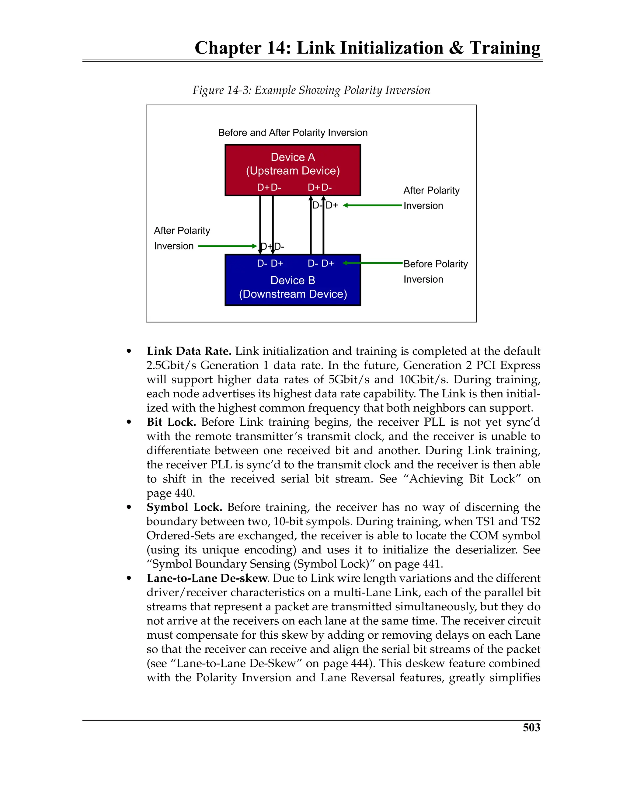
MindShare offers technical training courses to address companies' training needs in an effective and cost-efficient manner. They provide scalable, customizable training that can be delivered globally in various formats, including classroom, virtual classroom, and eLearning modules. MindShare has over 25 years of experience conducting training on cutting-edge technologies and works with many large technology companies. Their goal is to effectively transfer knowledge through engaging instruction.


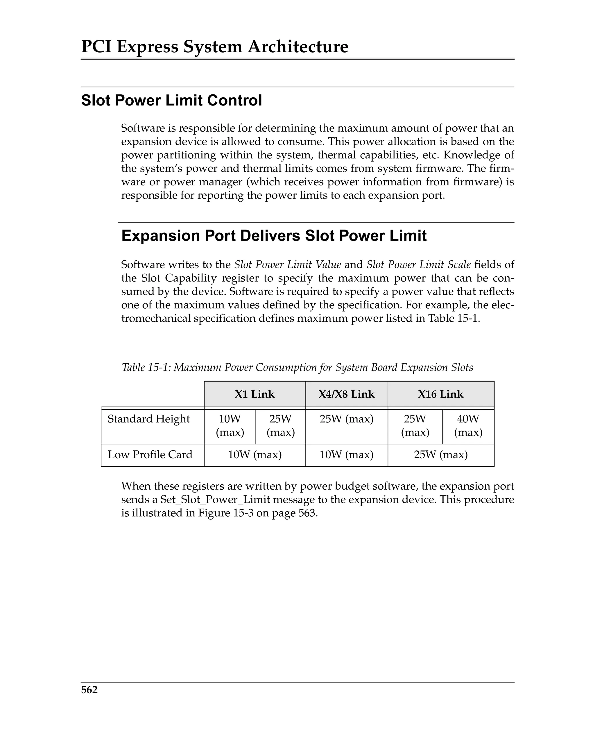
![Contents
xxv
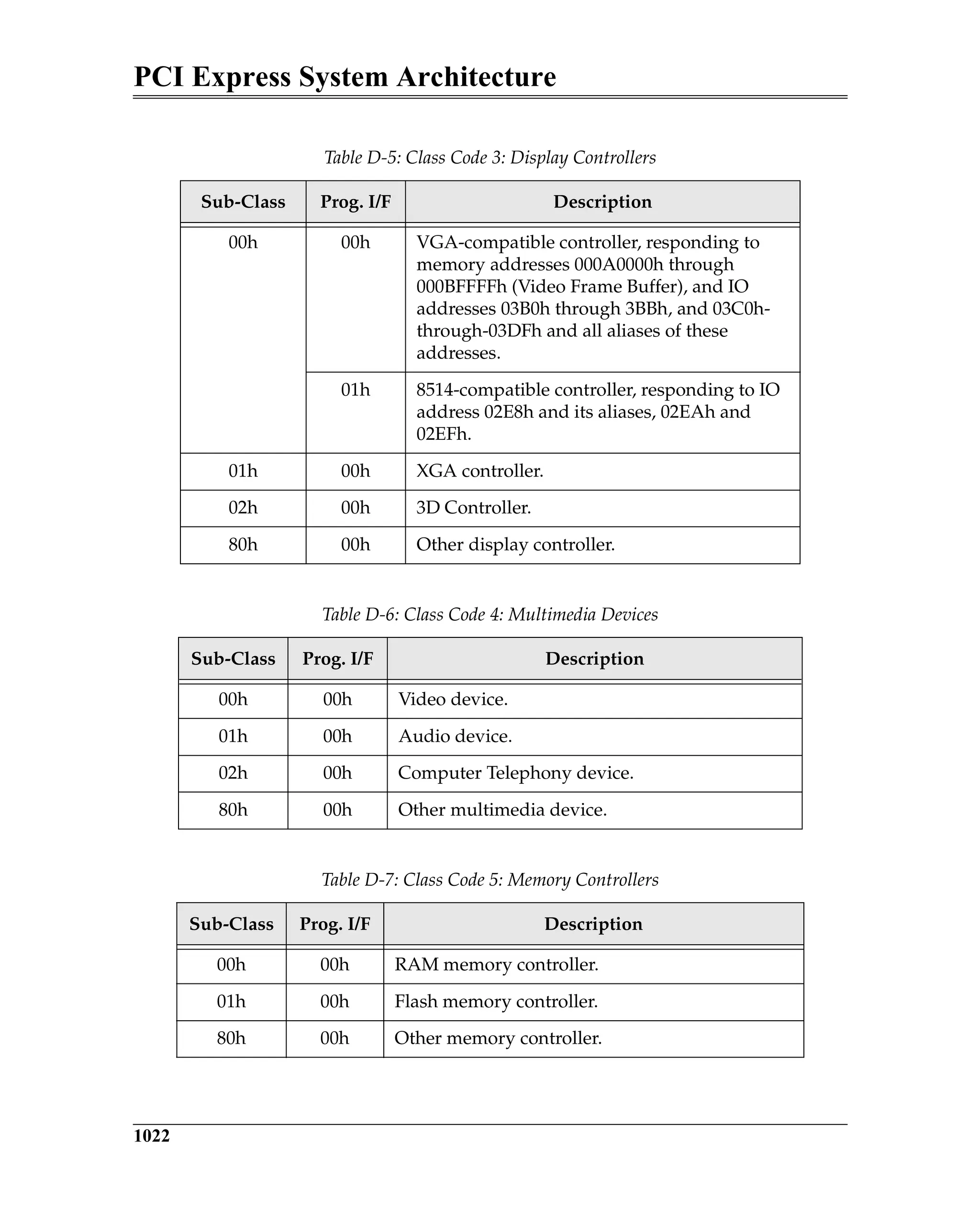
L2.Idle SubState......................................................................................................... 543
L1.TransmitWake SubState ..................................................................................... 543
Hot Reset State.................................................................................................................. 544
Disable State...................................................................................................................... 545
Loopback State ................................................................................................................. 547
Loopback.Entry SubState......................................................................................... 547
Loopback.Active SubState....................................................................................... 548
Loopback.Exit SubState............................................................................................ 548
LTSSM Related Configuration Registers.......................................................................... 549
Link Capability Register ................................................................................................. 549
Maximum Link Speed[3:0] ...................................................................................... 549
Maximum Link Width[9:4]...................................................................................... 550
Link Status Register......................................................................................................... 551
Link Speed[3:0]:......................................................................................................... 551
Negotiate Link Width[9:4]....................................................................................... 551
Training Error[10]..................................................................................................... 551
Link Training[11] ...................................................................................................... 551
Link Control Register ...................................................................................................... 552
Link Disable............................................................................................................... 552
Retrain Link ............................................................................................................... 552
Extended Synch......................................................................................................... 552
Part Four: Power-Related Topics
Chapter 15: Power Budgeting
Introduction to Power Budgeting ....................................................................................... 557
The Power Budgeting Elements.......................................................................................... 558
Slot Power Limit Control...................................................................................................... 562
Expansion Port Delivers Slot Power Limit................................................................... 562
Expansion Device Limits Power Consumption........................................................... 564
The Power Budget Capabilities Register Set.................................................................... 564
Chapter 16: Power Management
Introduction............................................................................................................................. 568
Primer on Configuration Software ..................................................................................... 569
Basics of PCI PM .............................................................................................................. 569
OnNow Design Initiative Scheme Defines Overall PM ............................................. 571
Goals ........................................................................................................................... 572
System PM States...................................................................................................... 572
Device PM States....................................................................................................... 573
Definition of Device Context................................................................................... 574](https://image.slidesharecdn.com/pciexpresssystemarchitecture-240110064541-2f1f00b9/75/pci-express-system-architecture-pdf-24-2048.jpg)


![PCI Express System Architecture
212
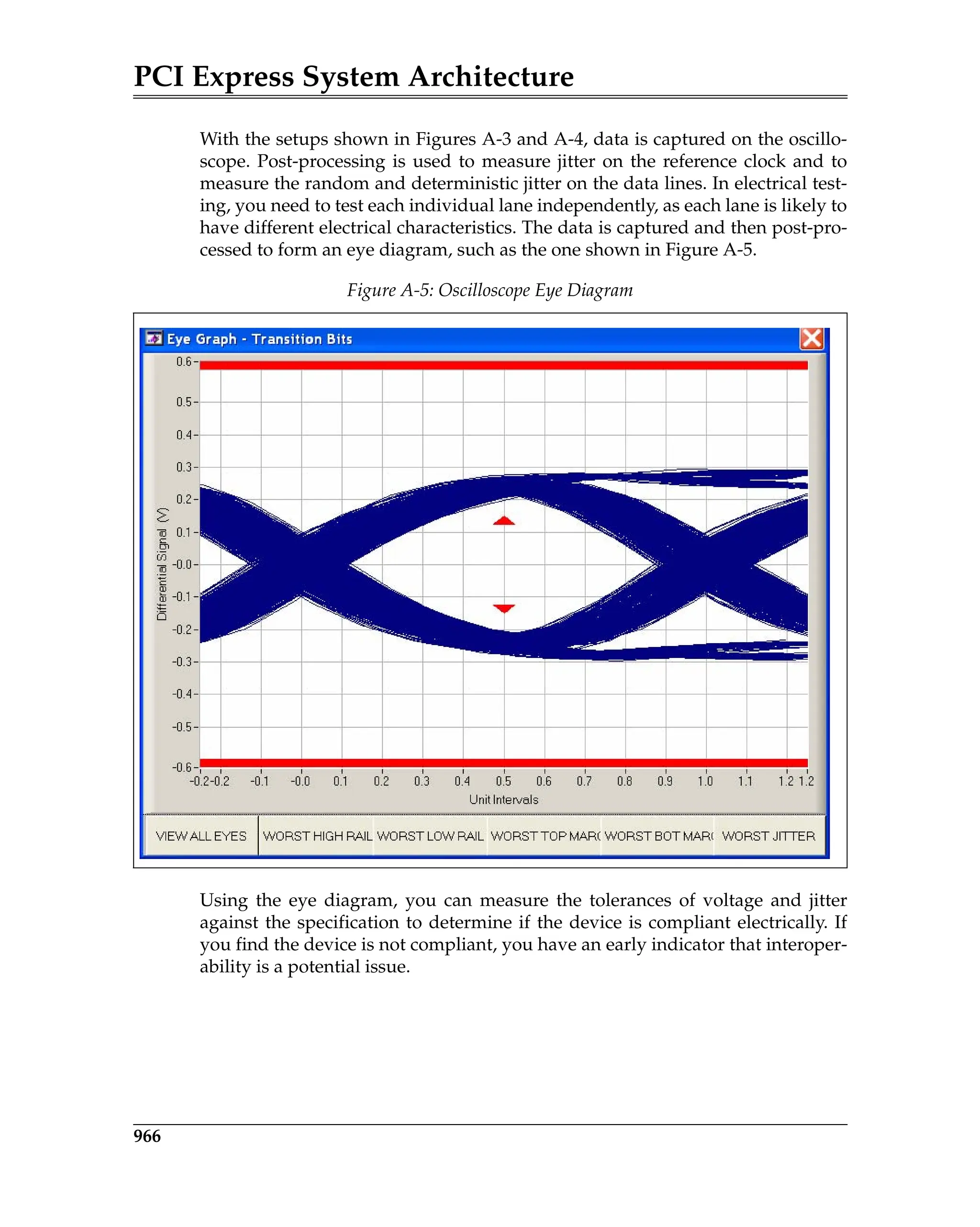
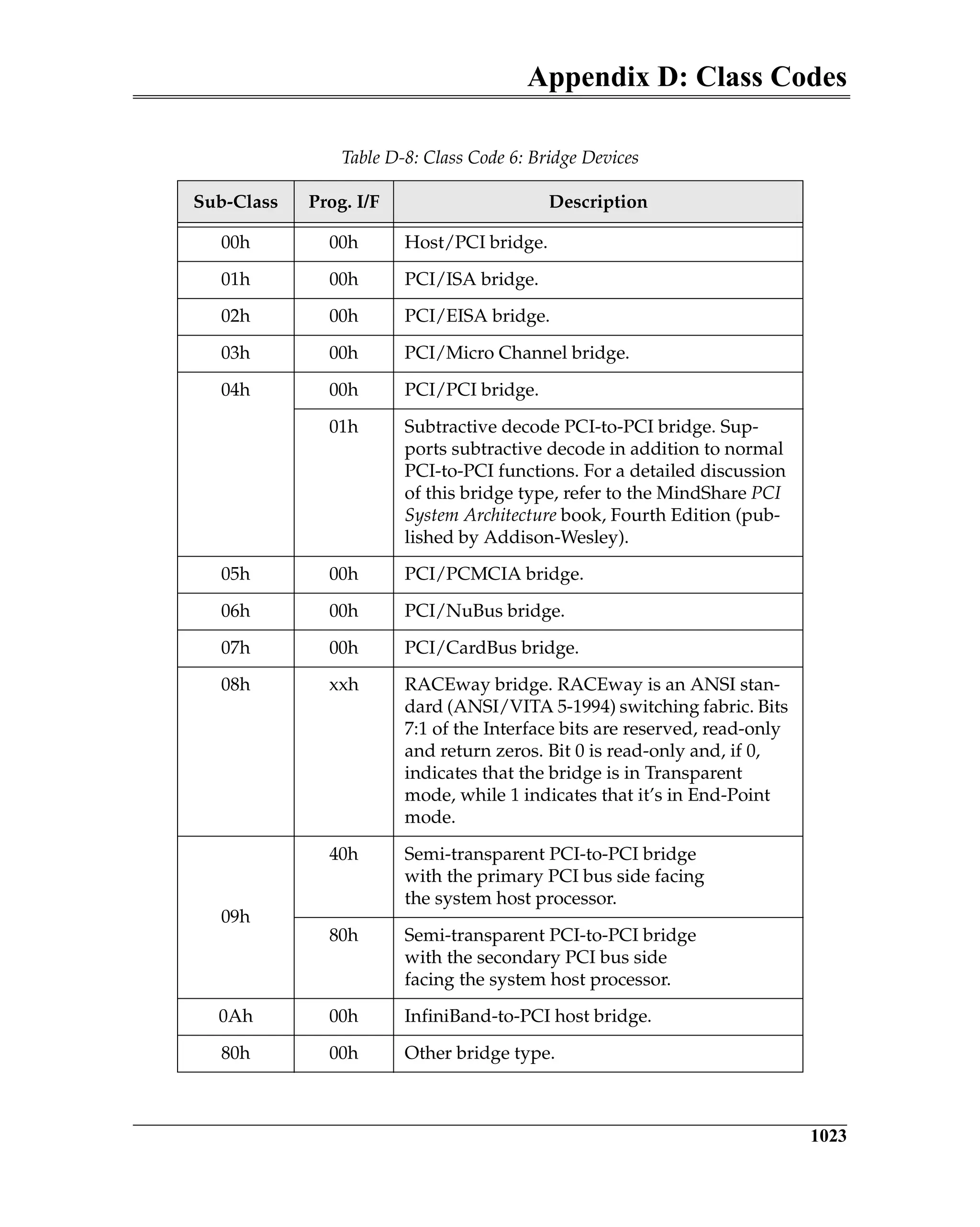
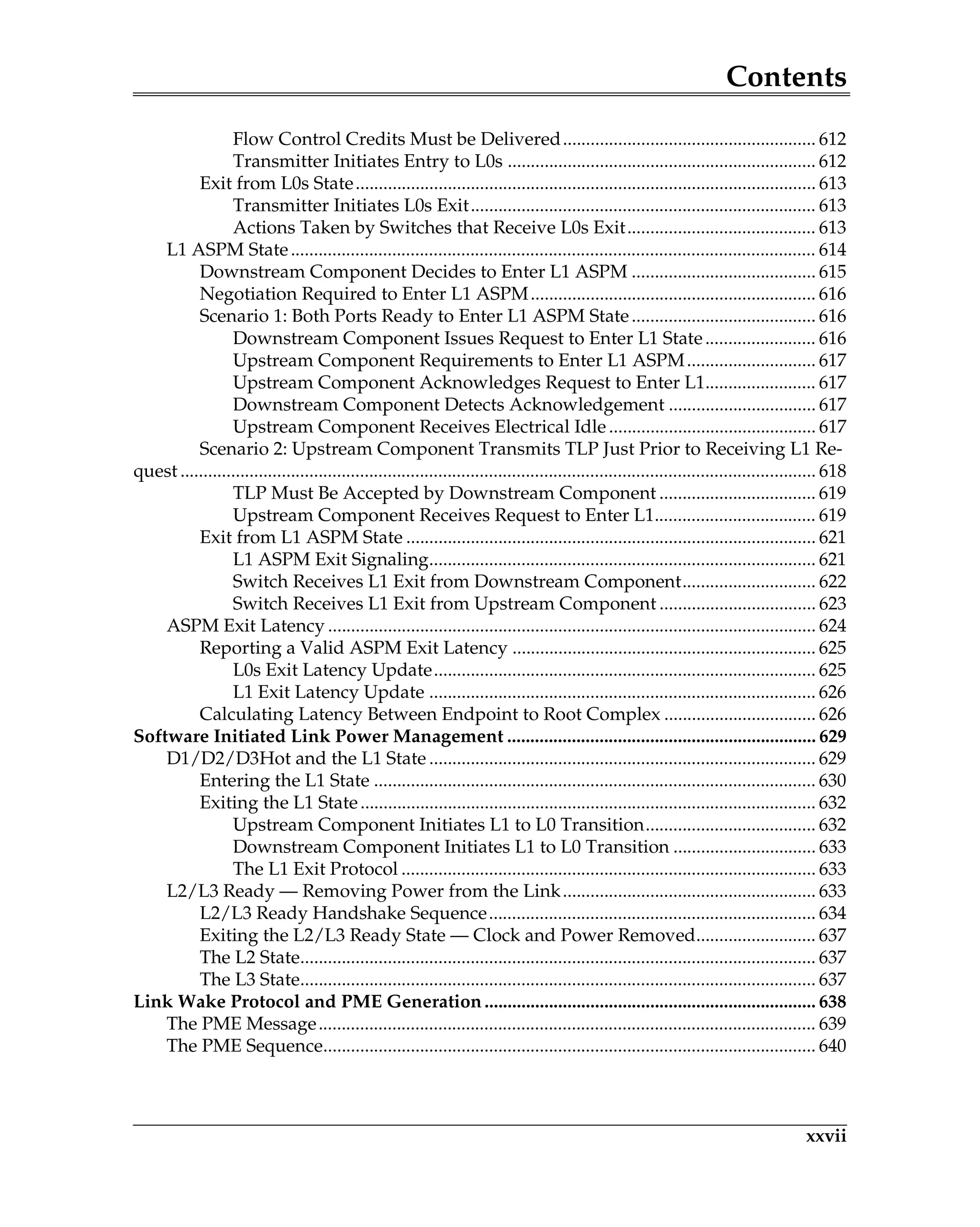
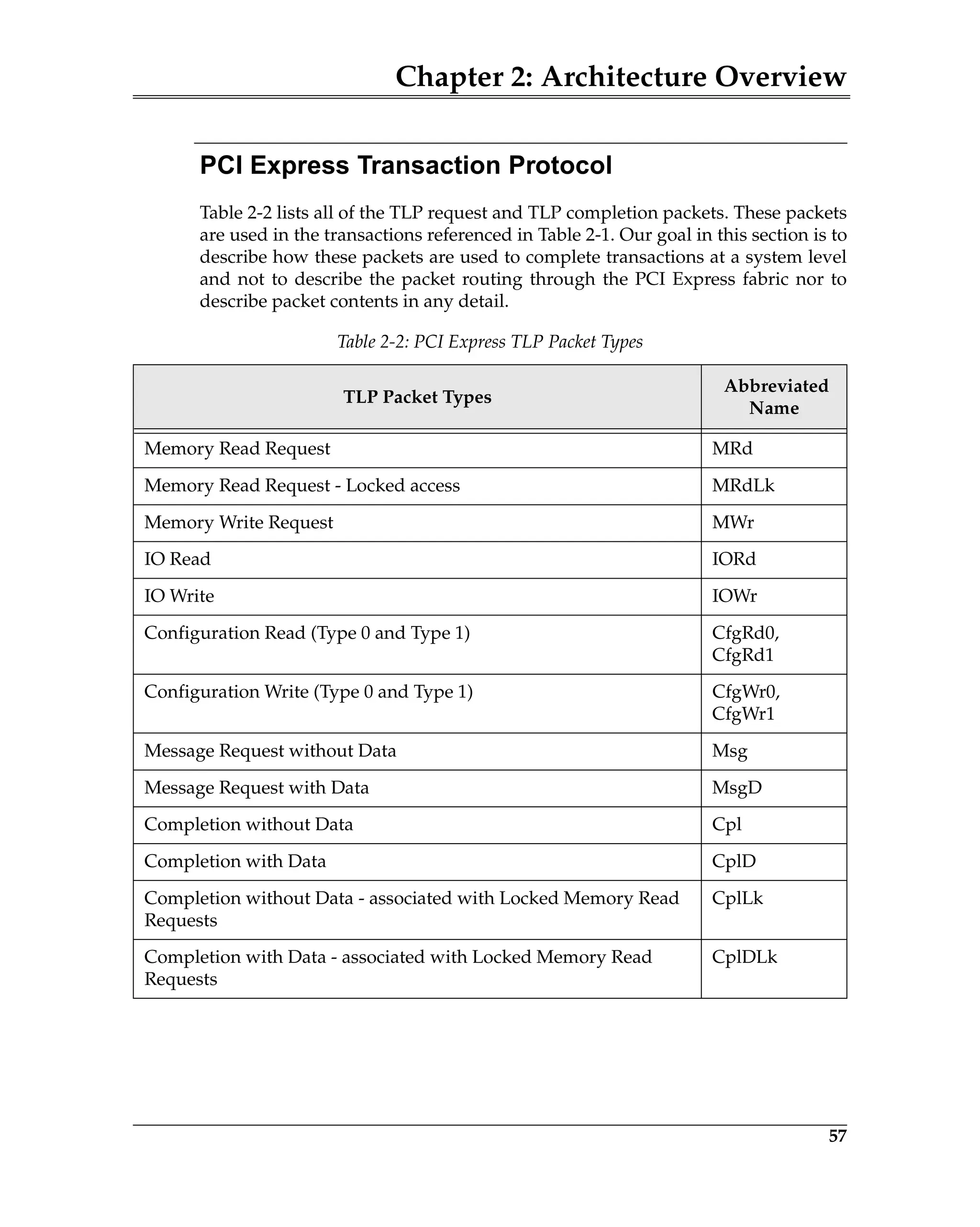
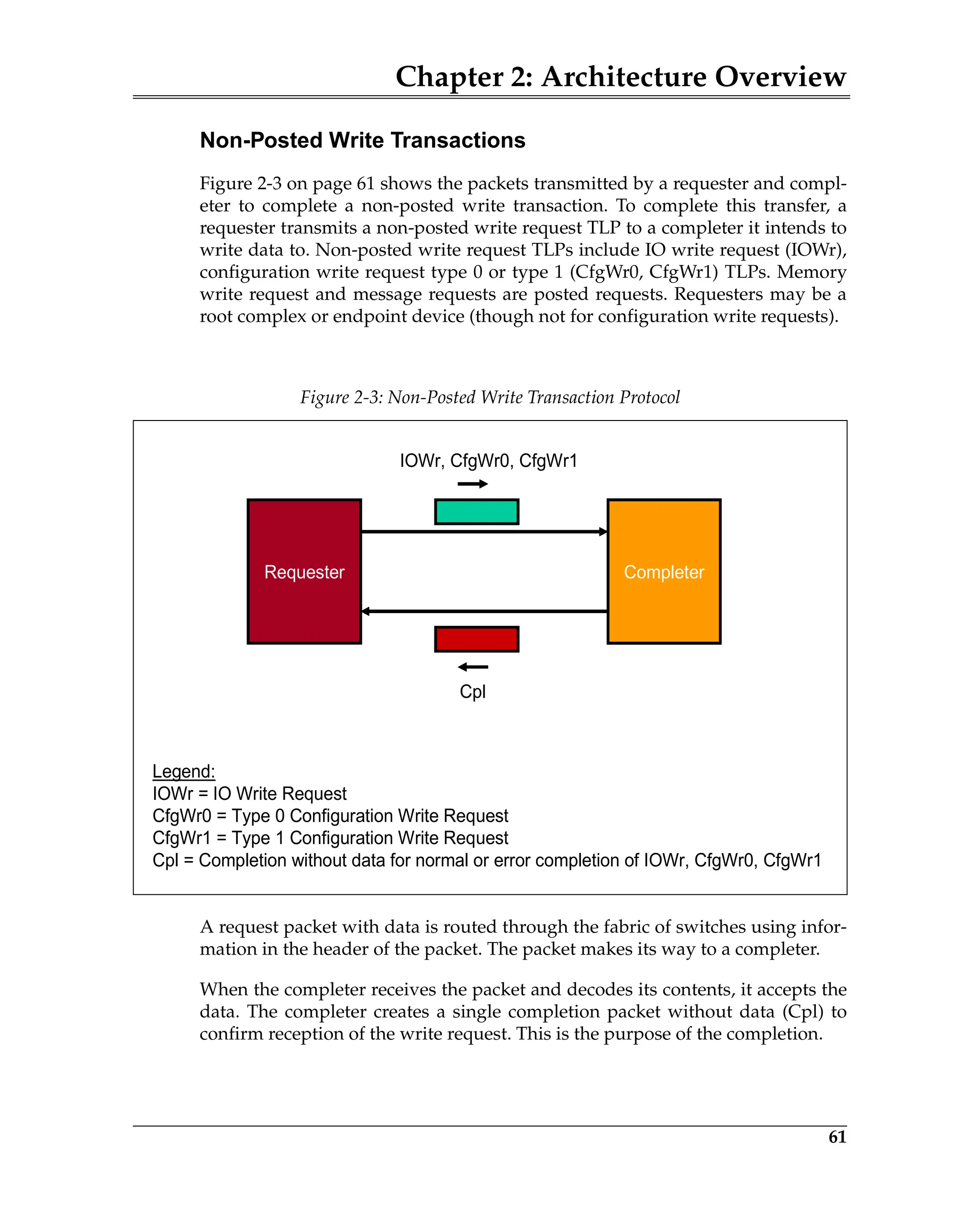
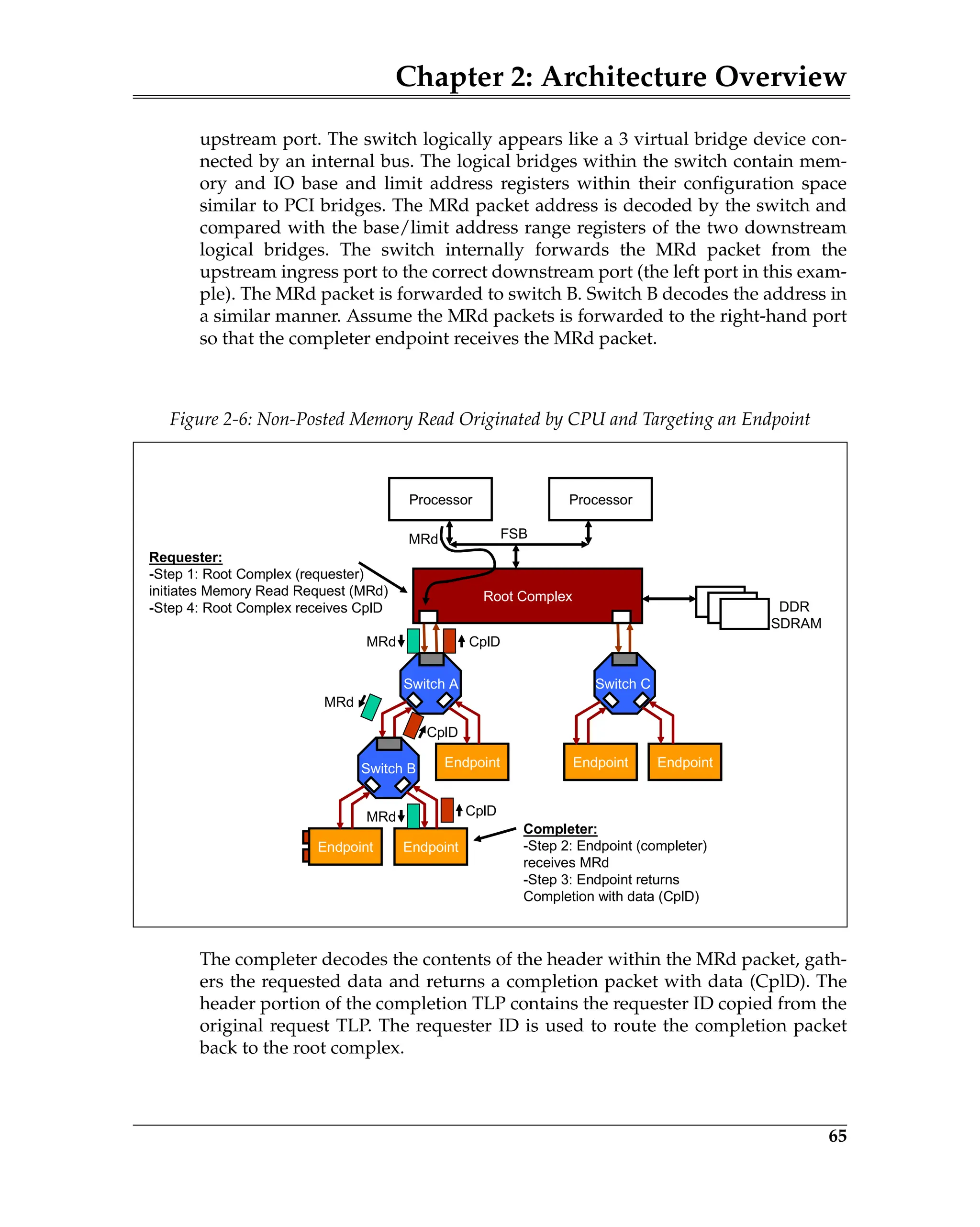
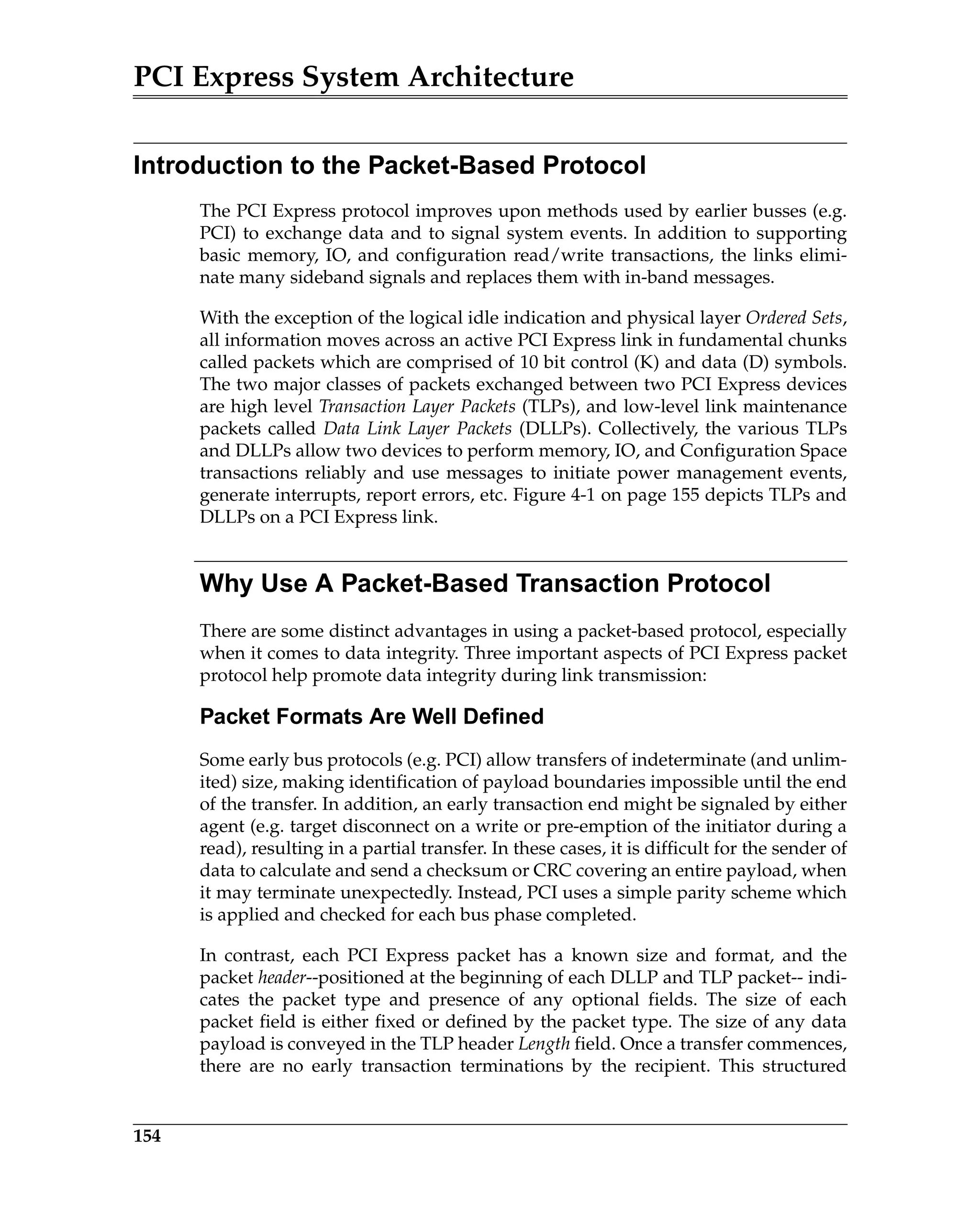
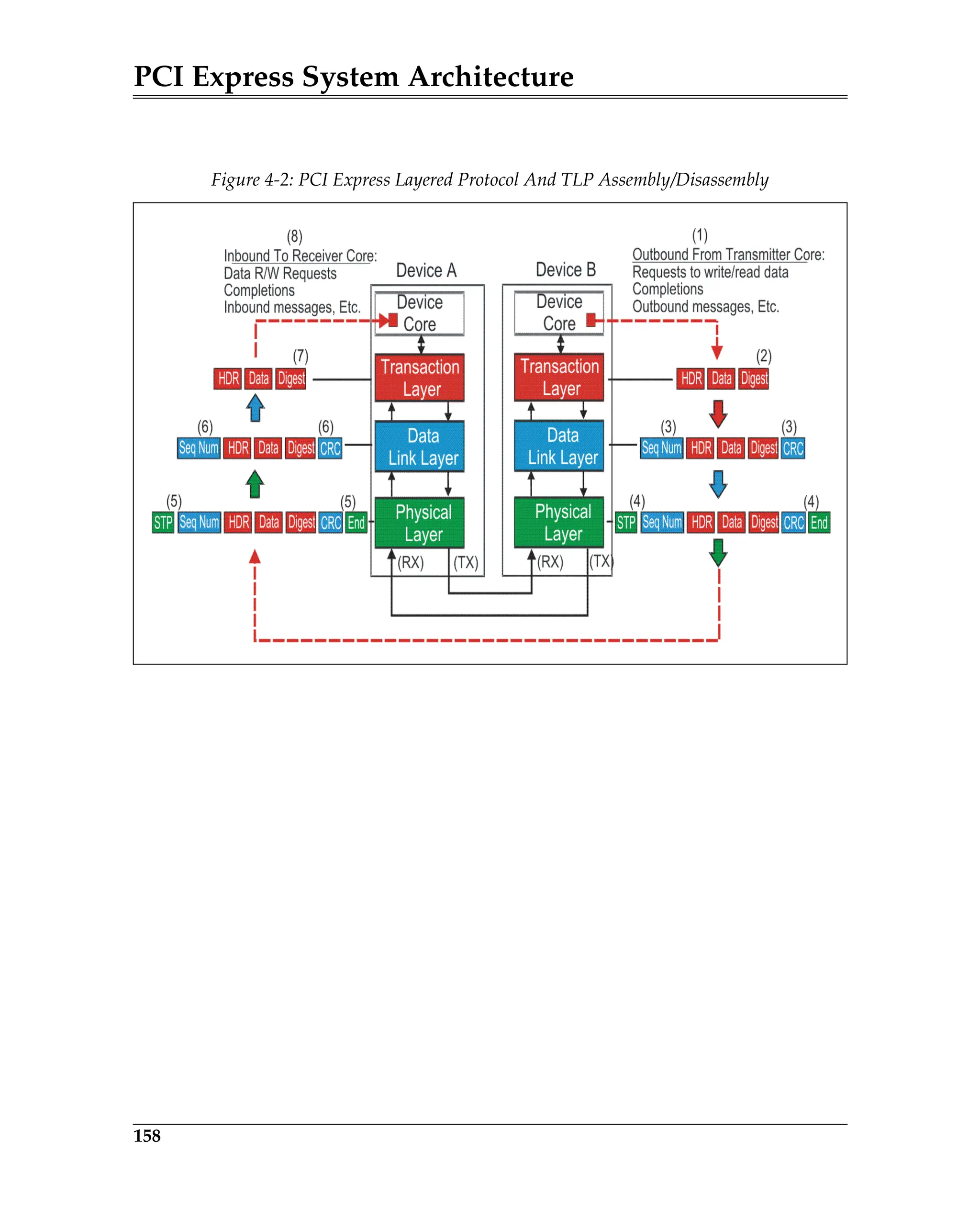
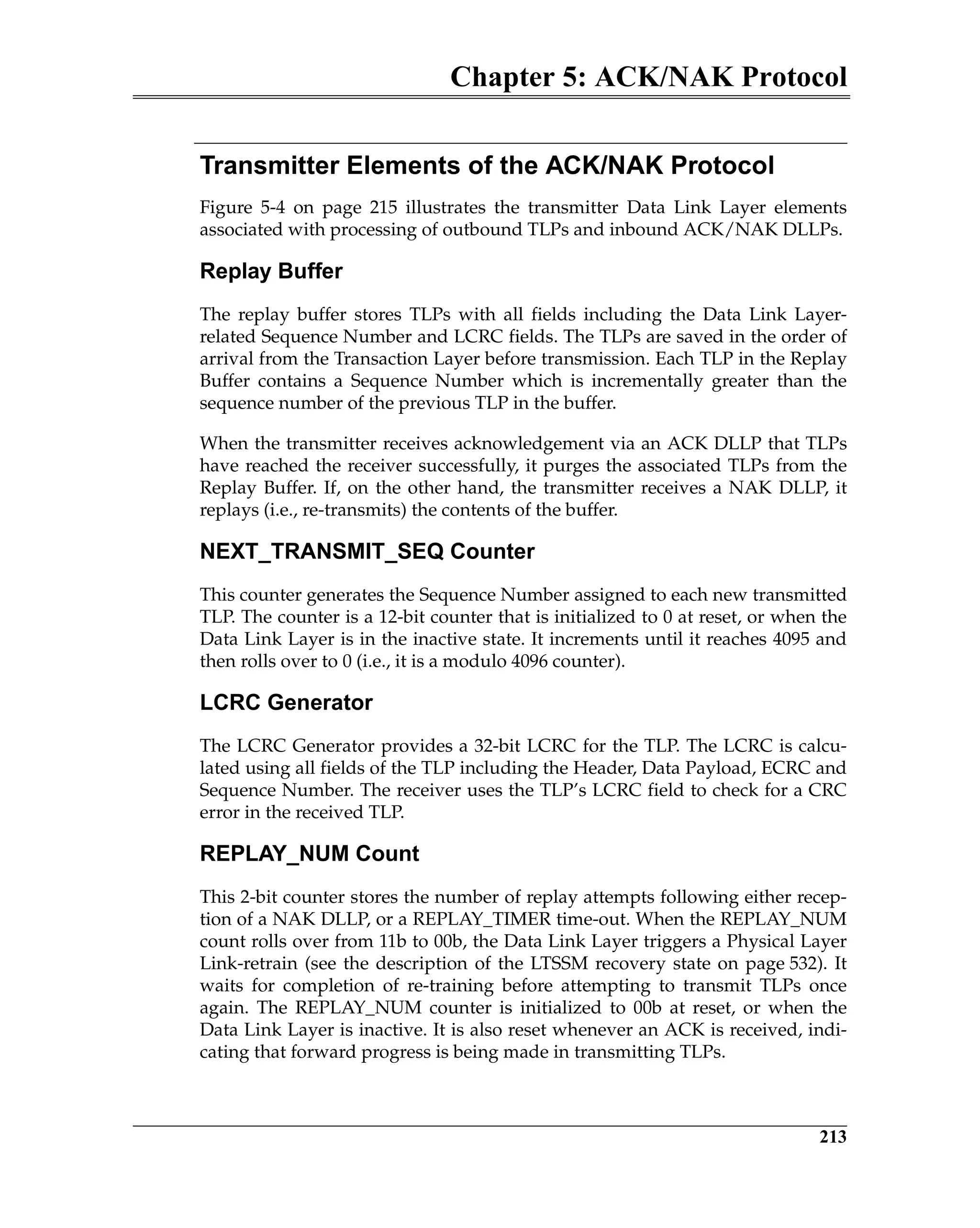
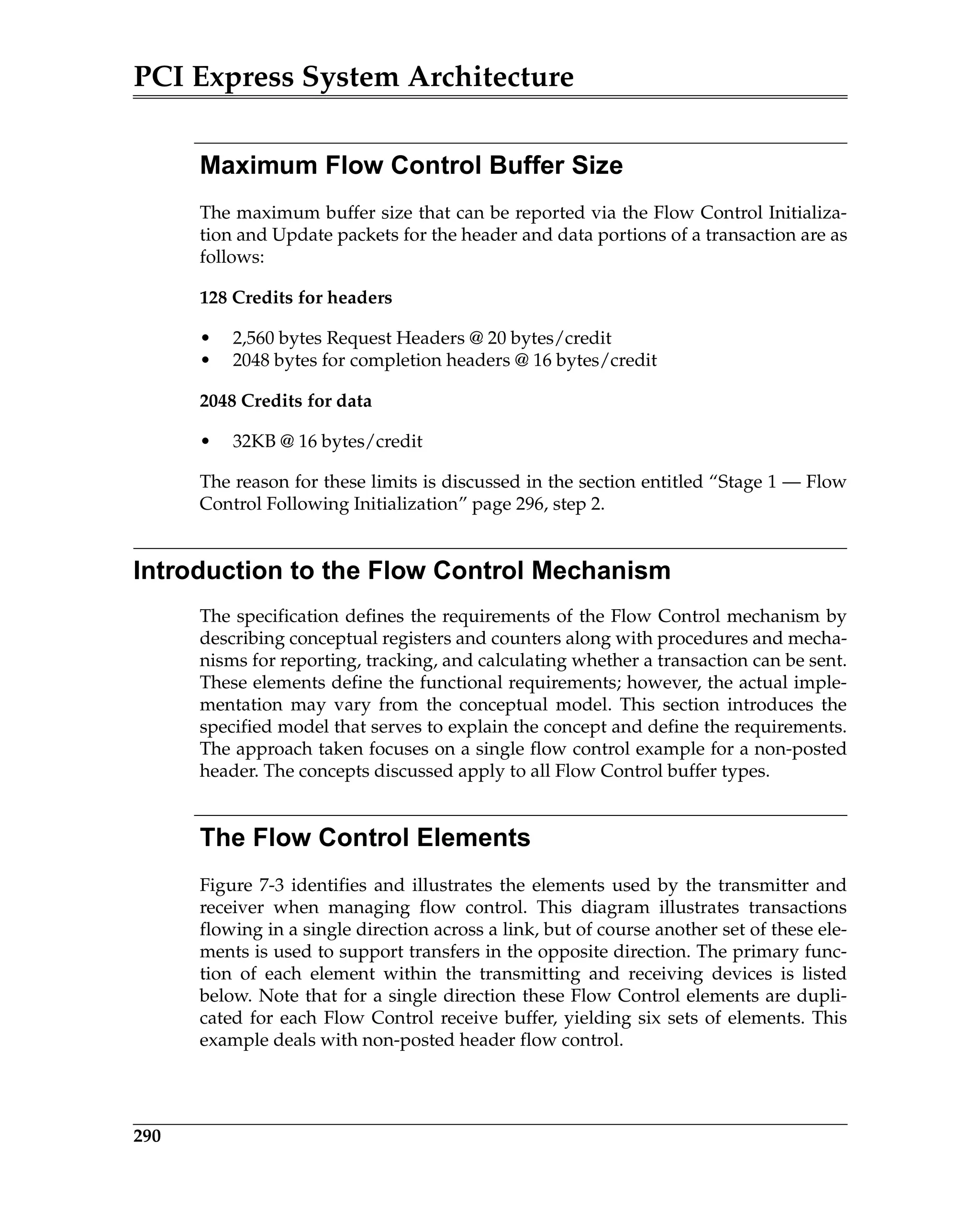
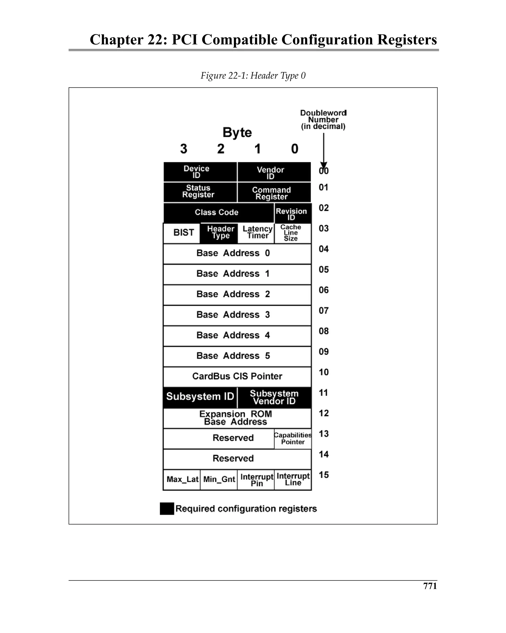
Elements of the ACK/NAK Protocol
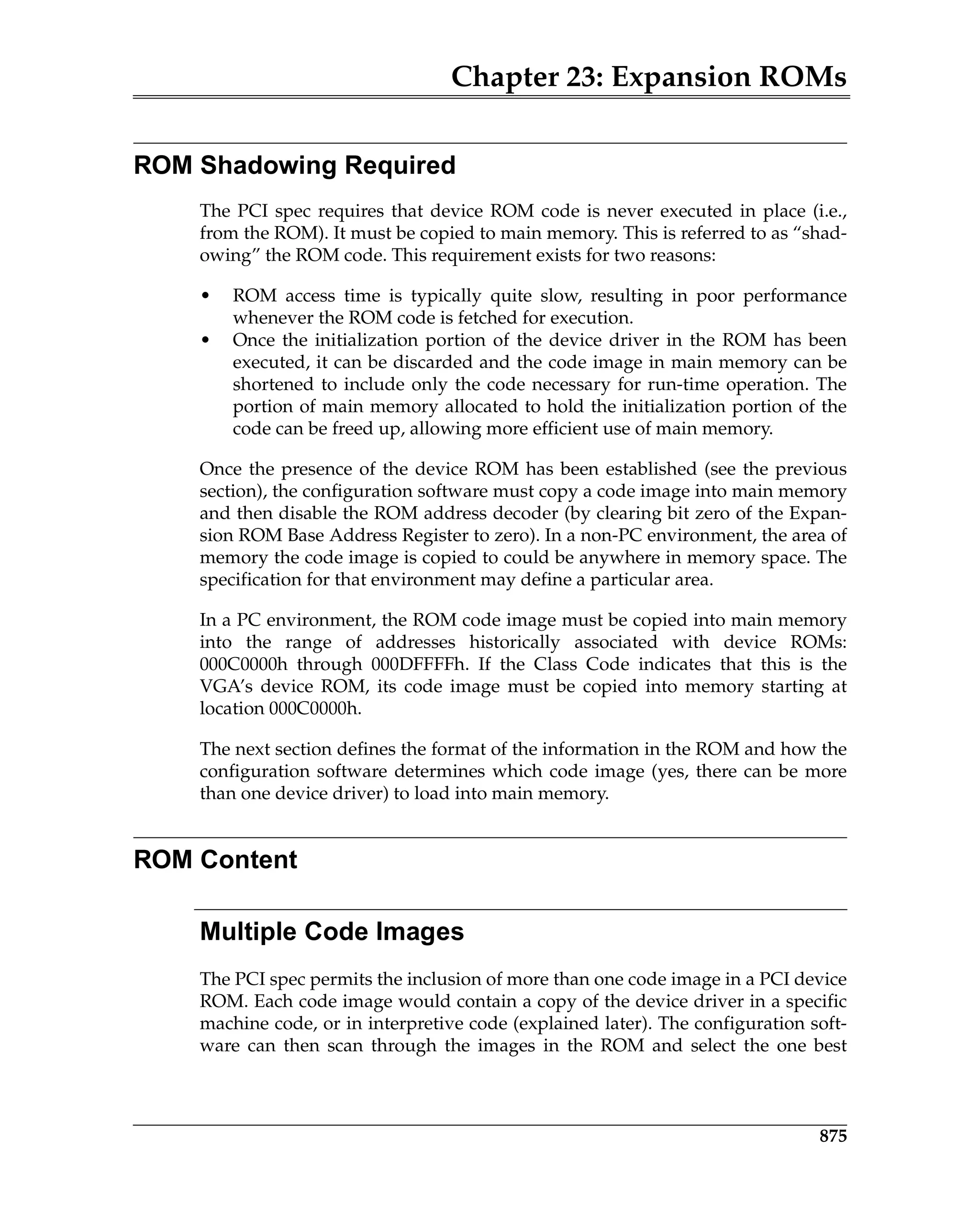
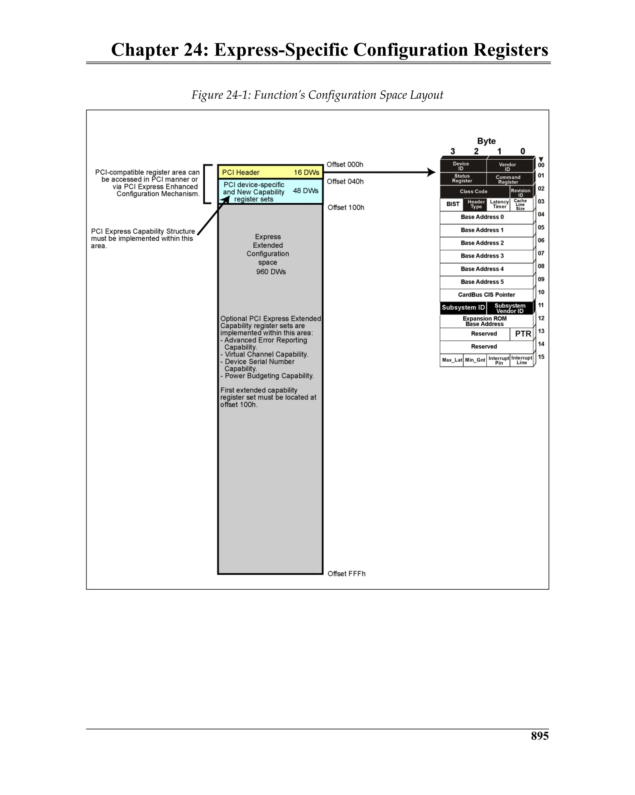
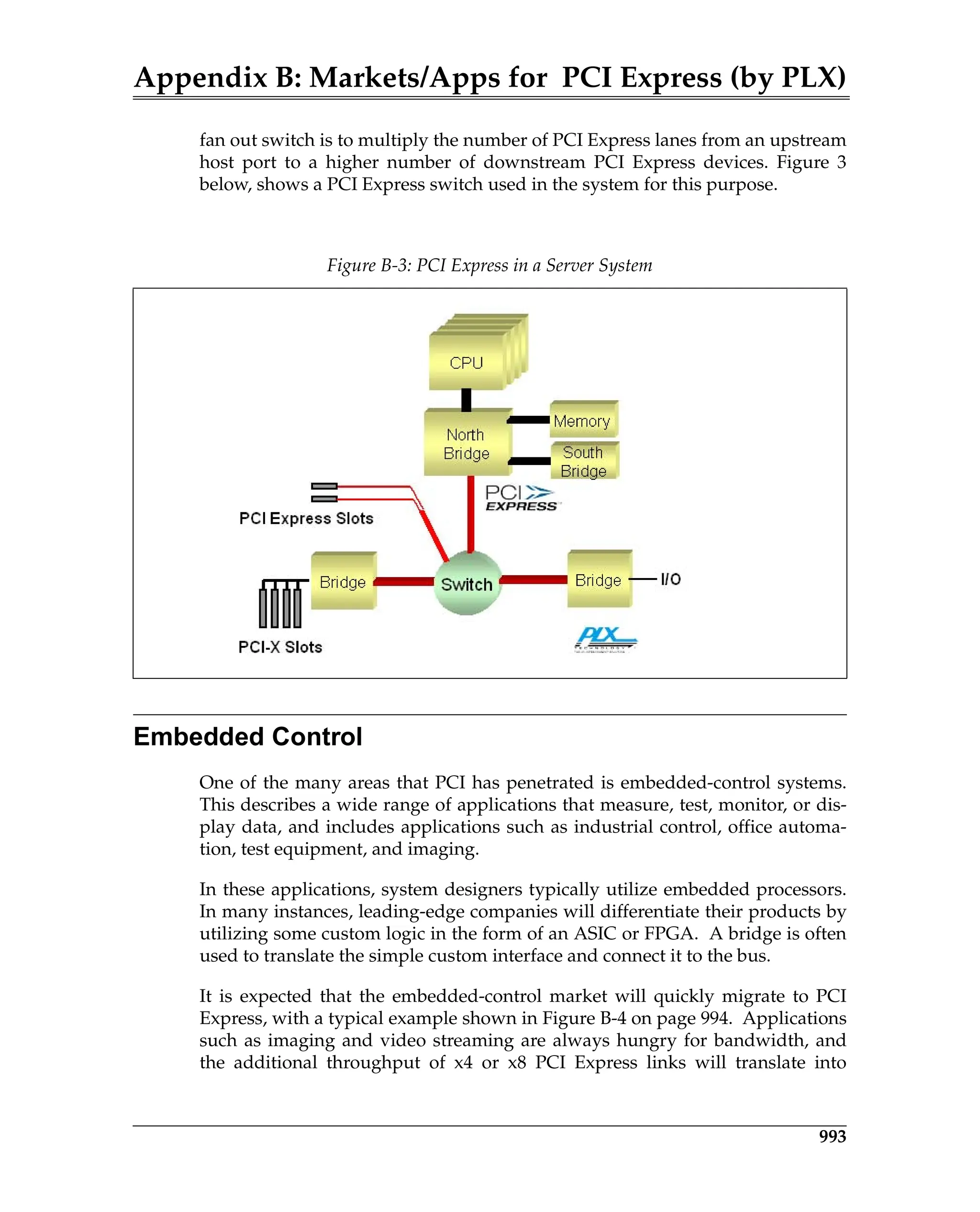
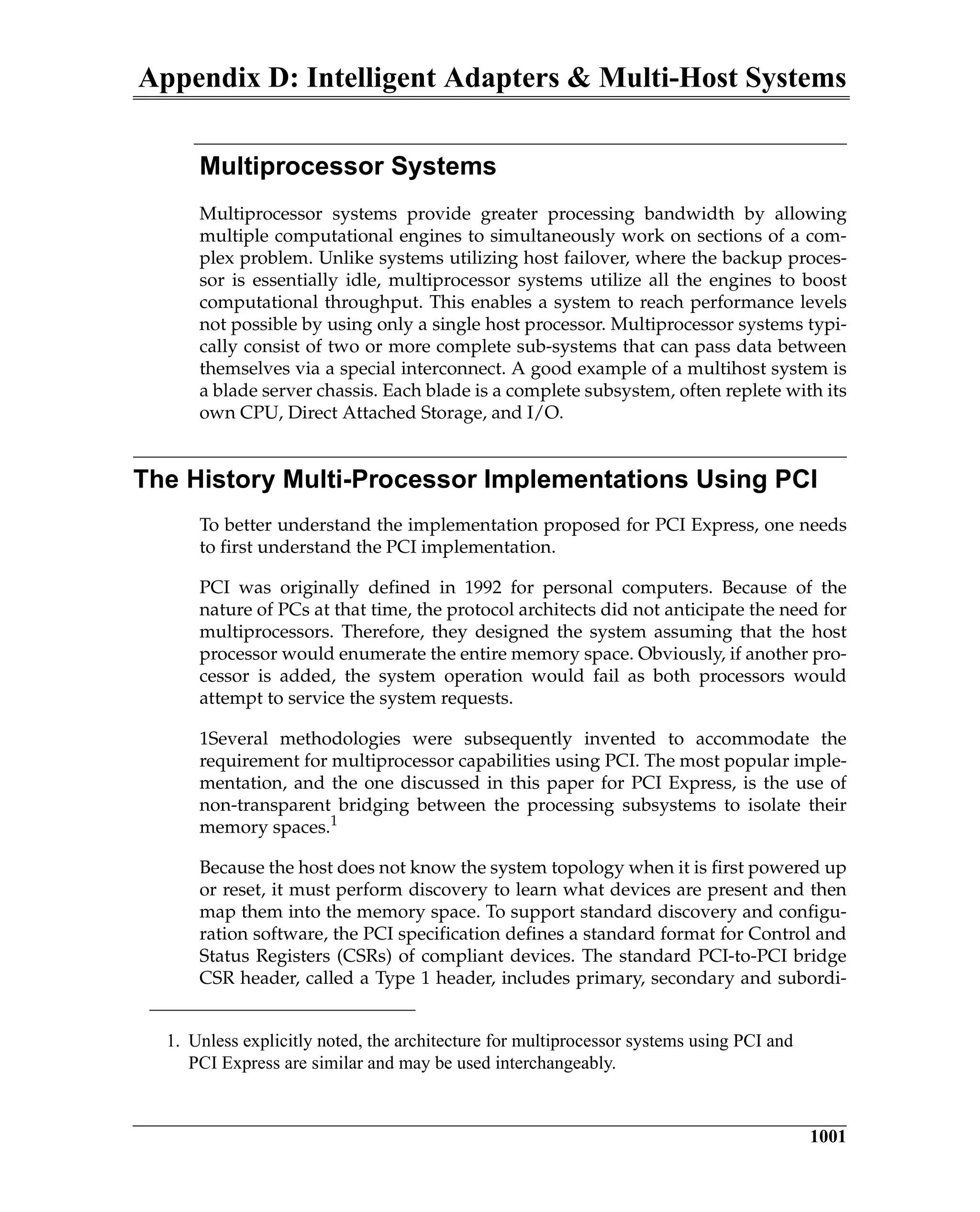
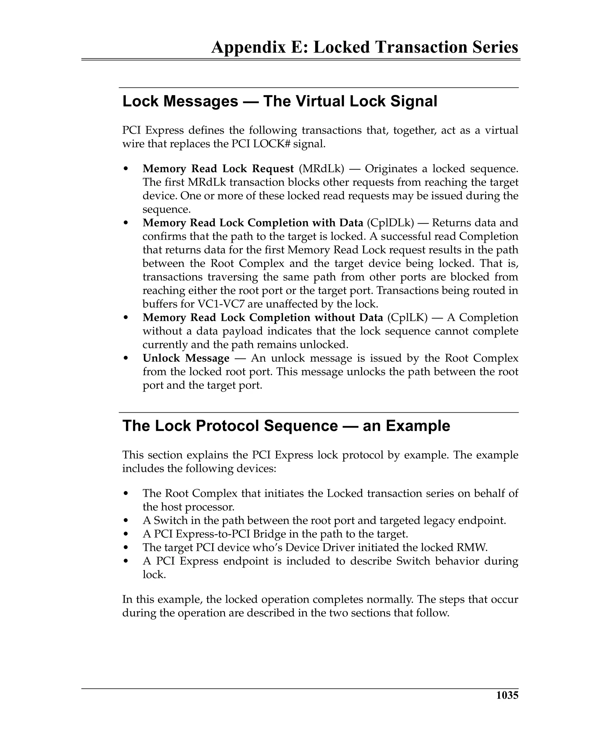
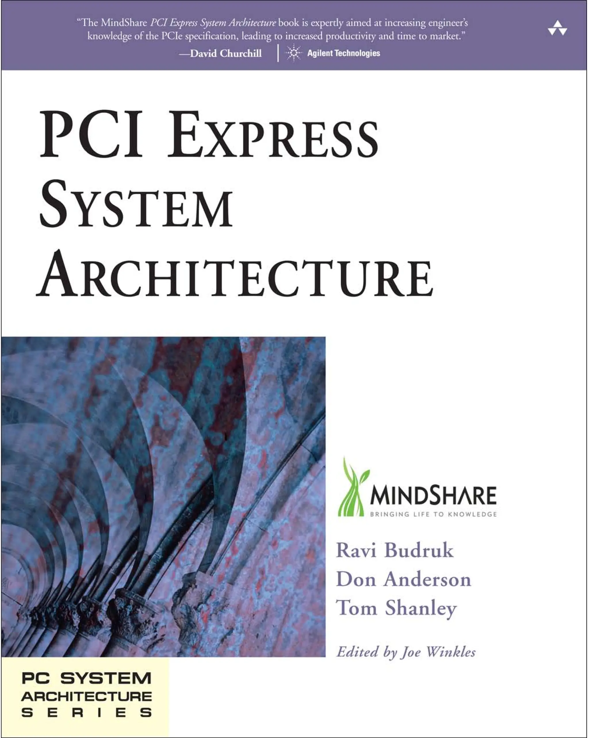
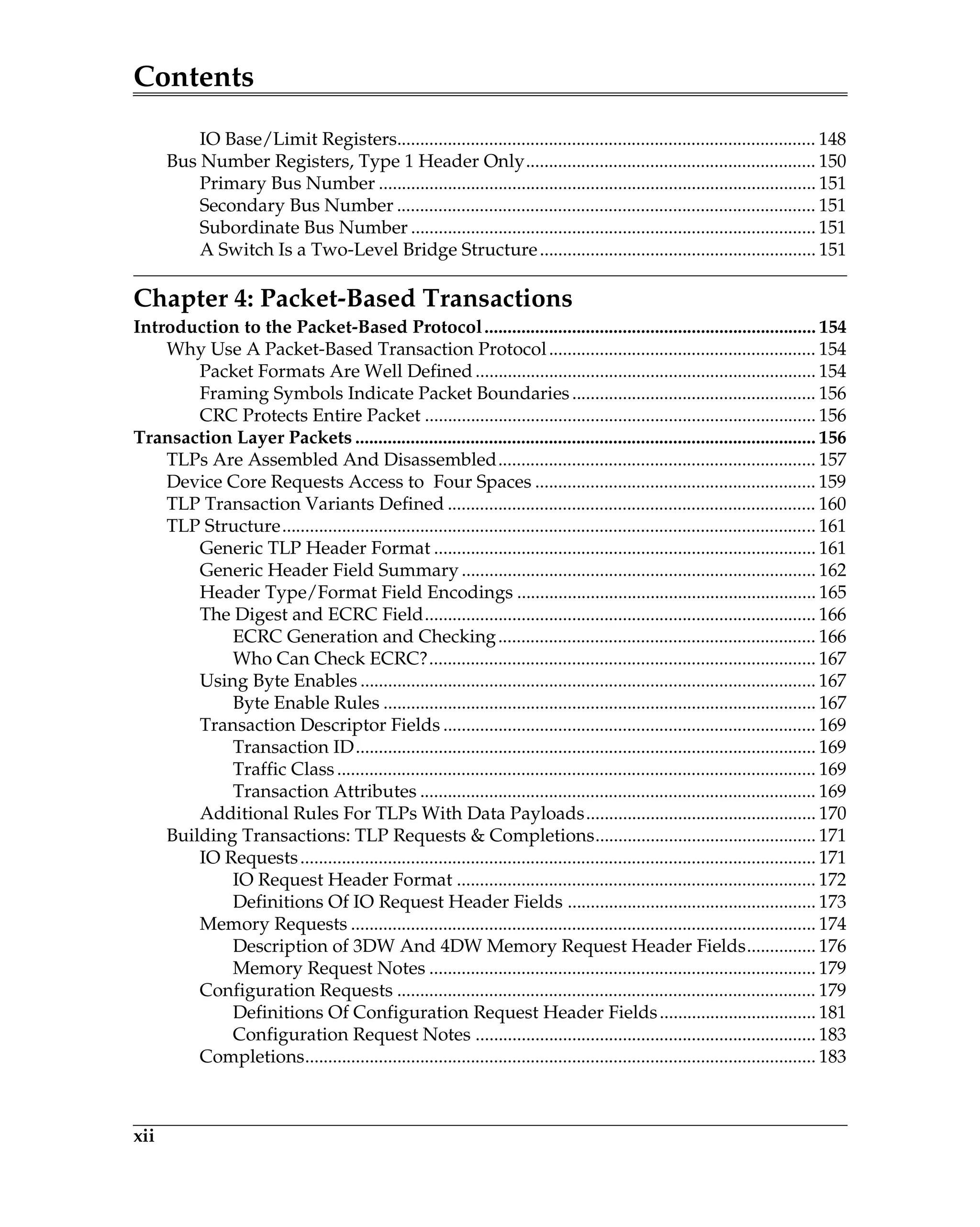
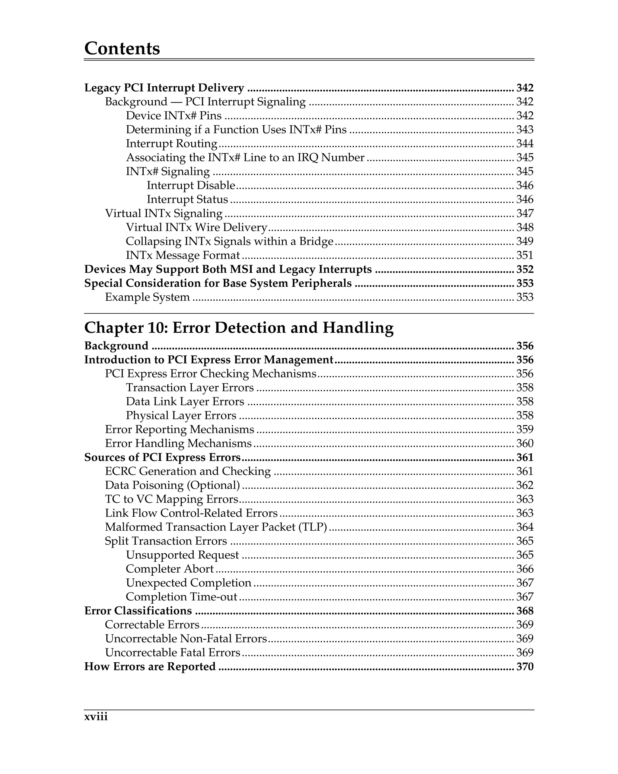
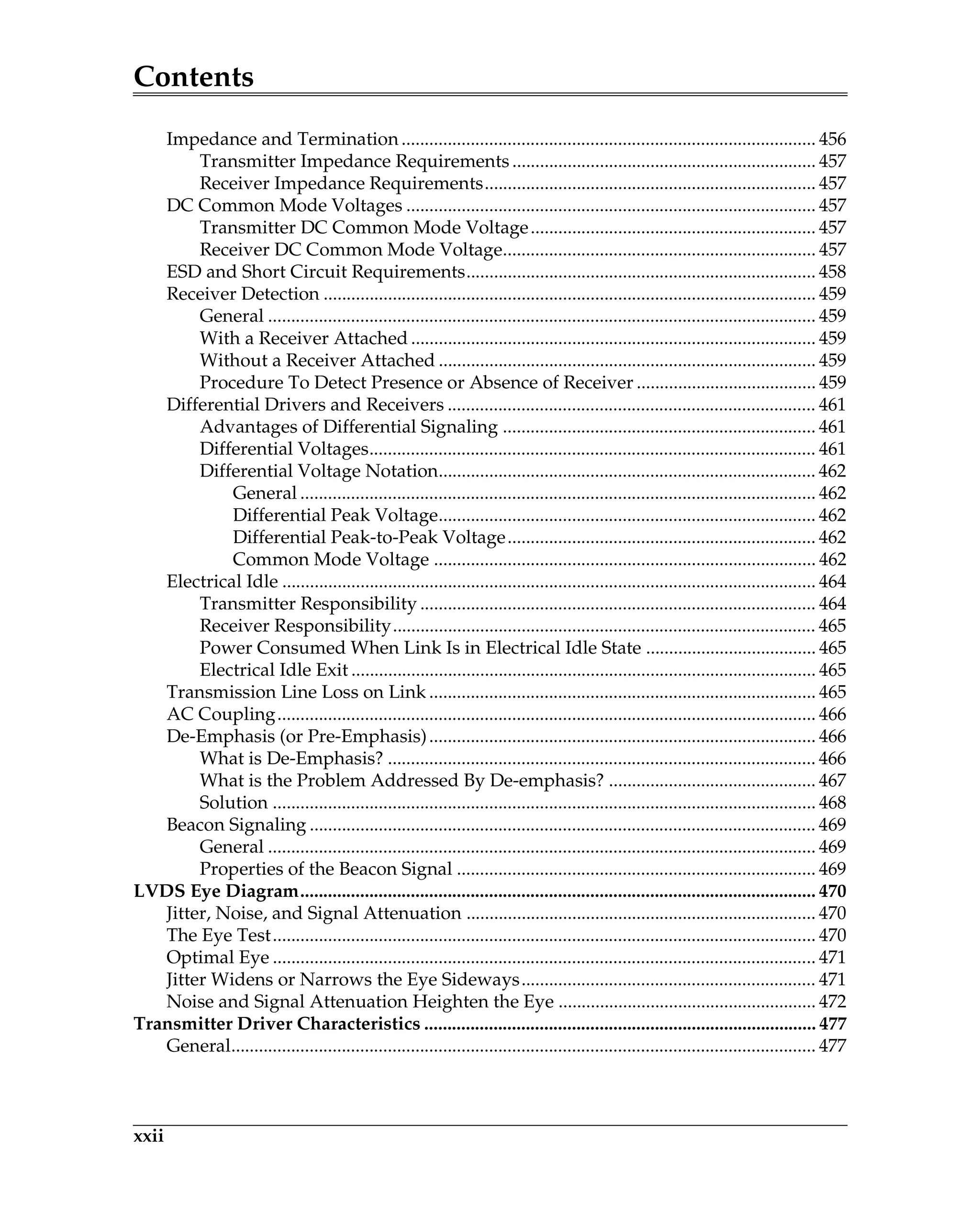
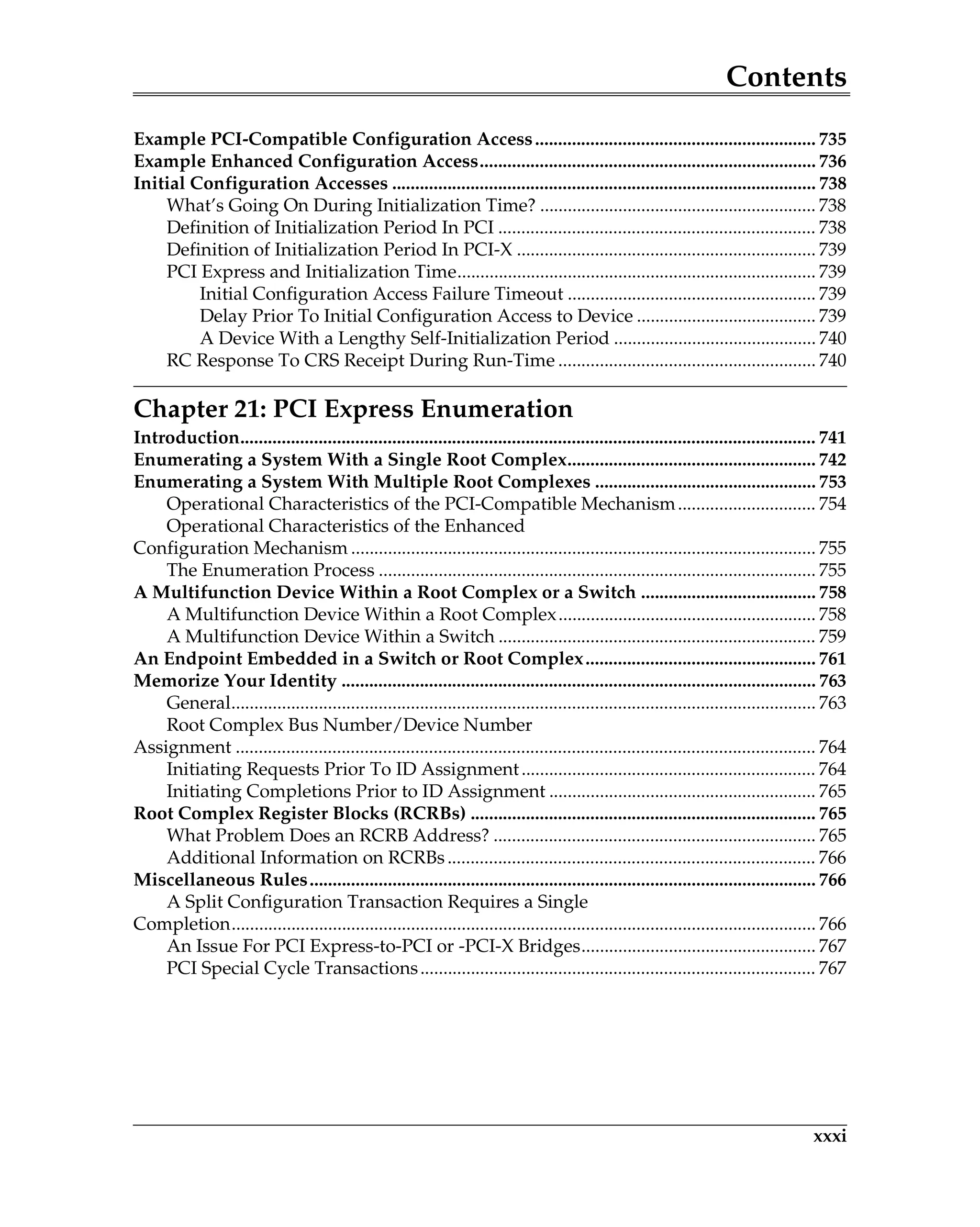
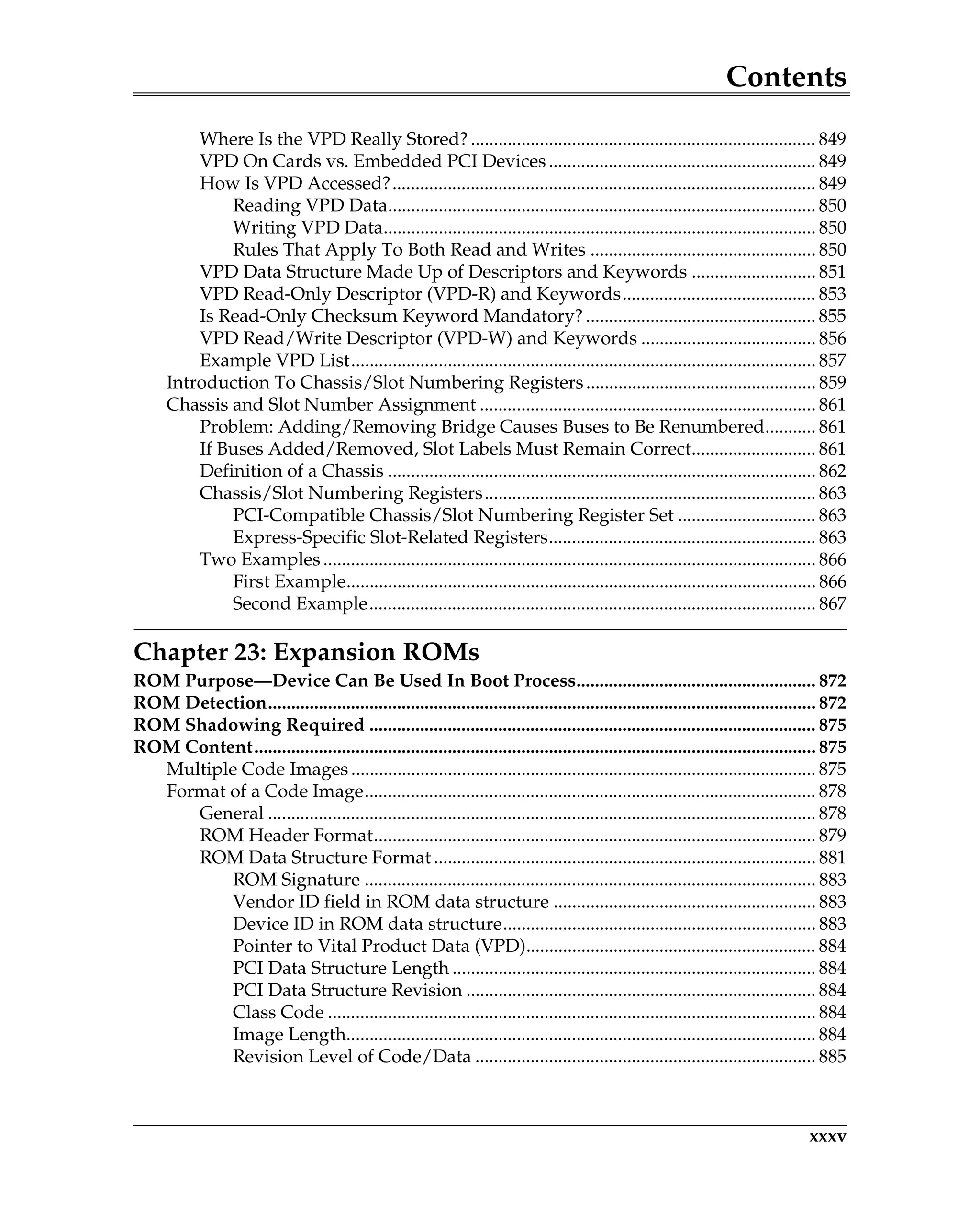
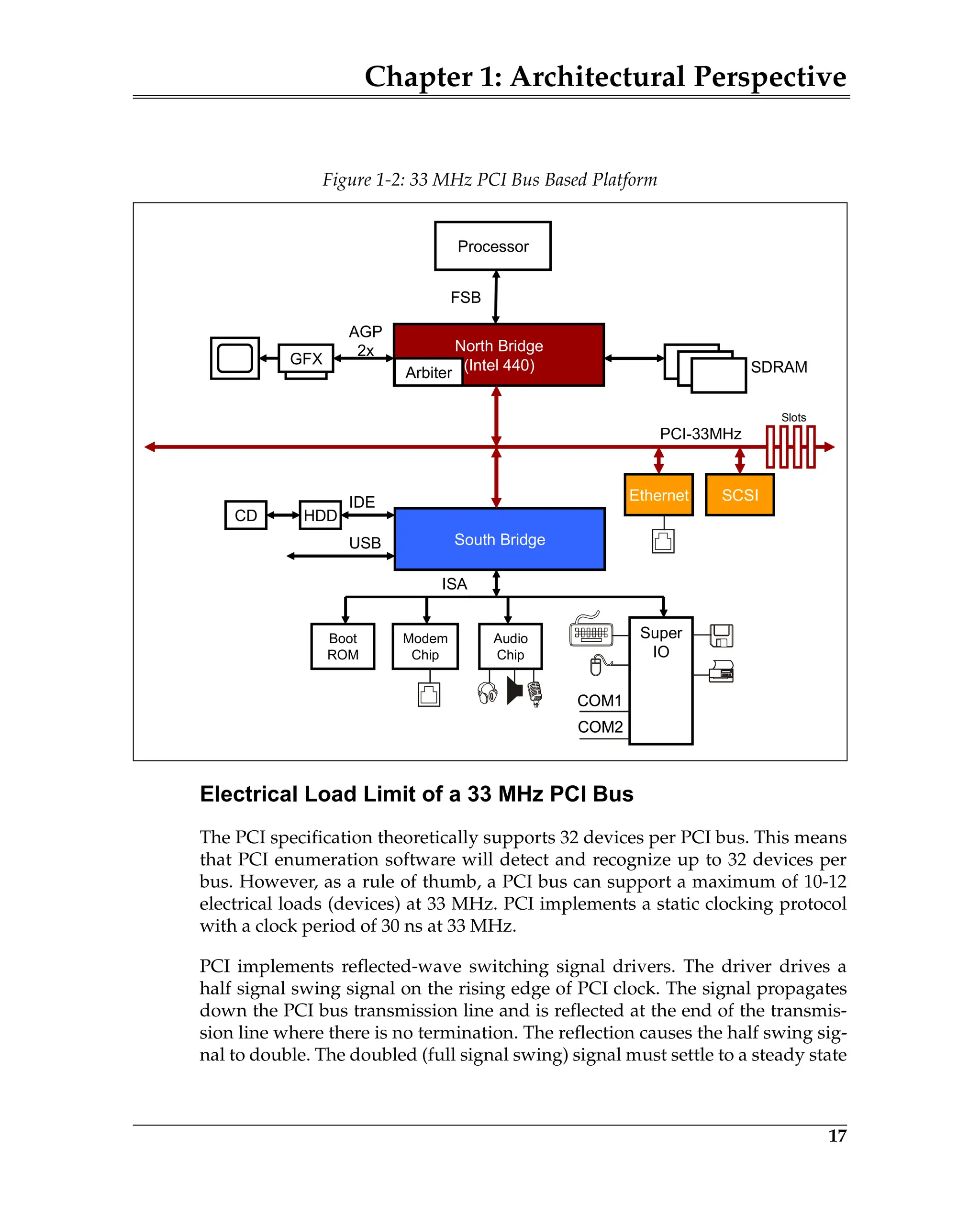
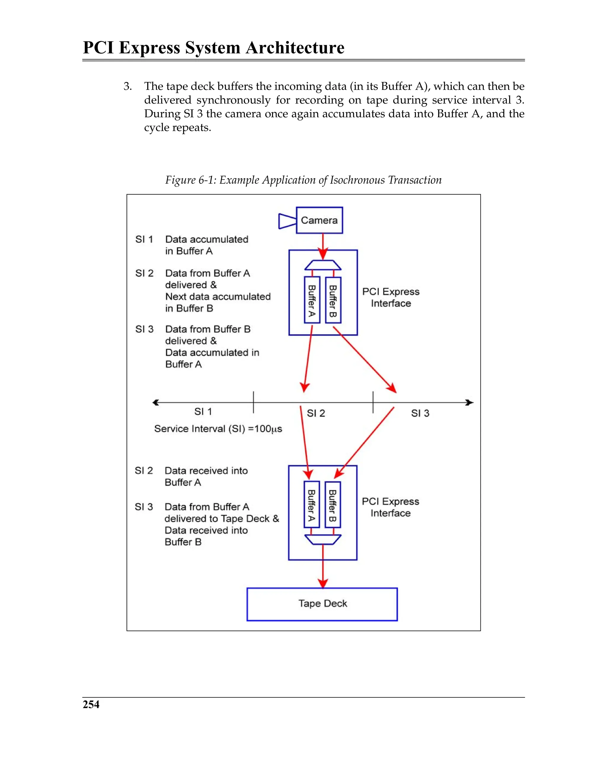
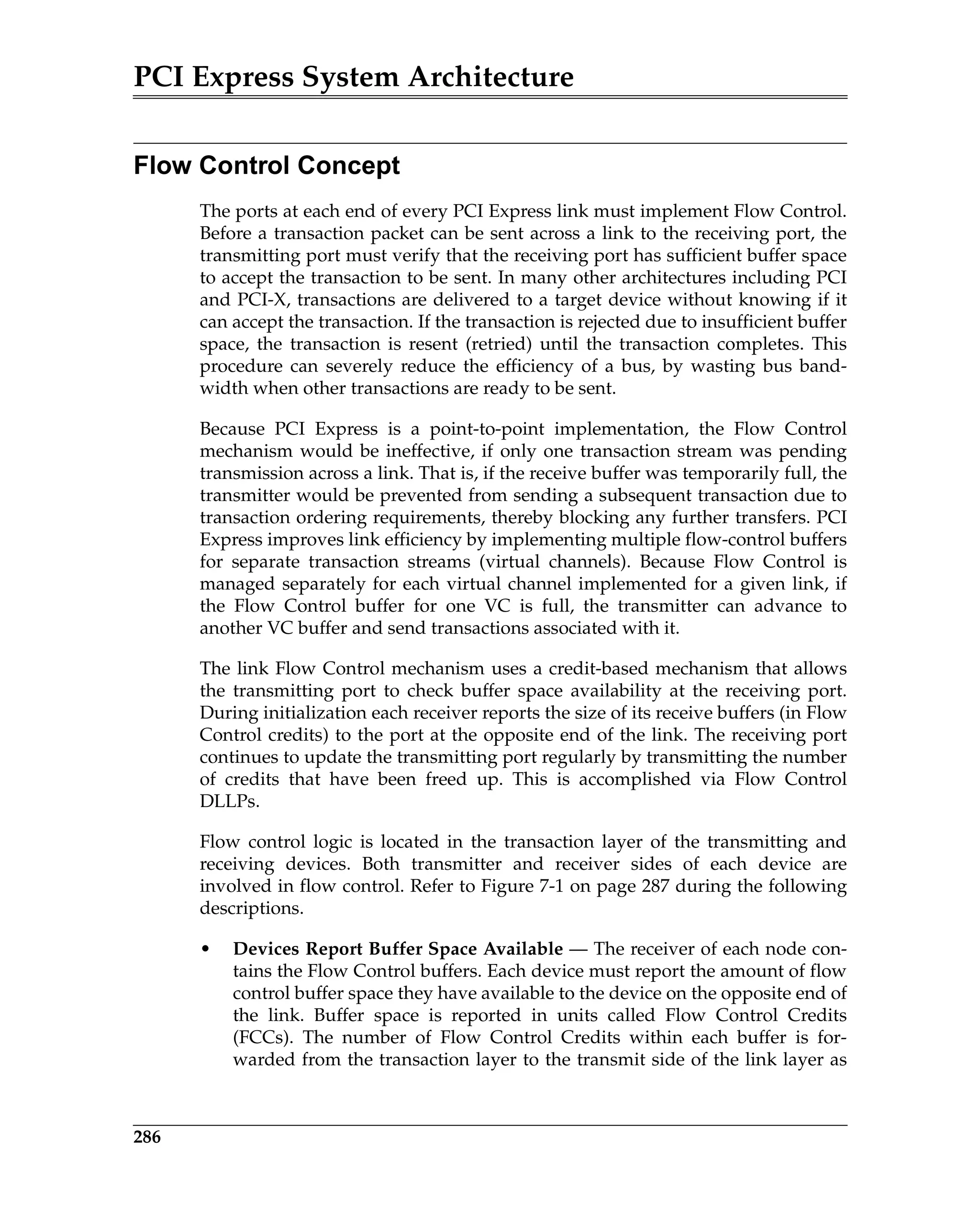
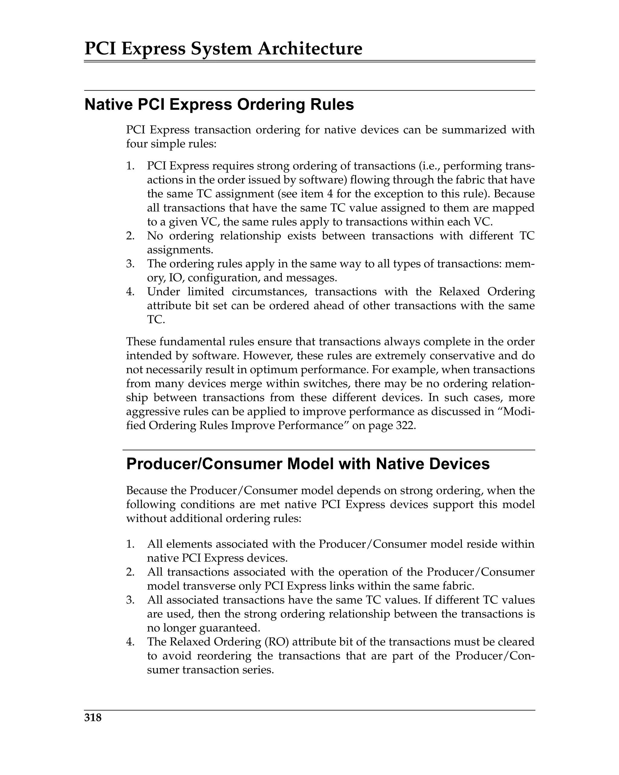
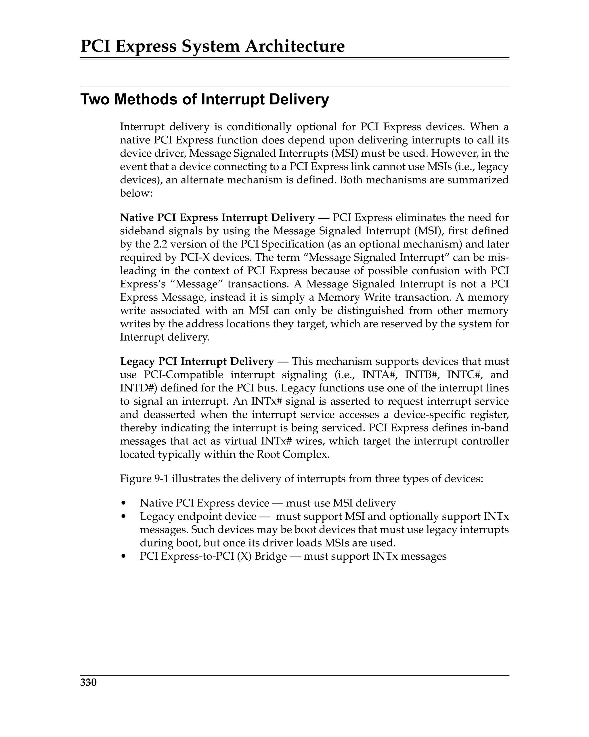
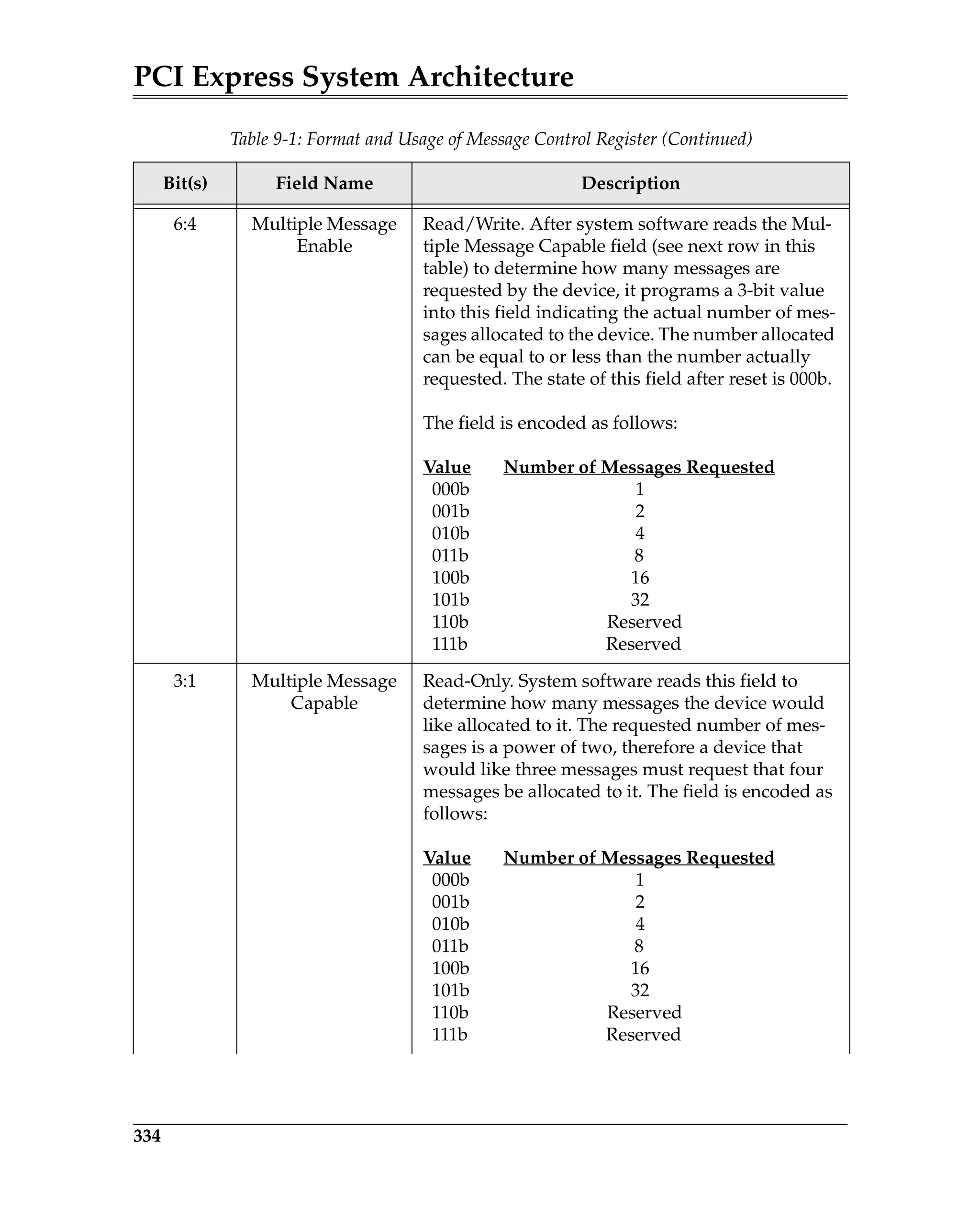
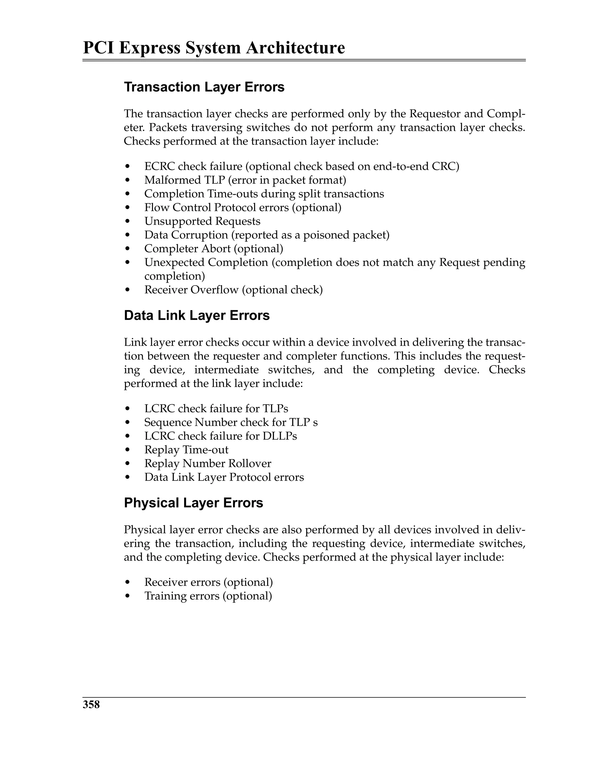
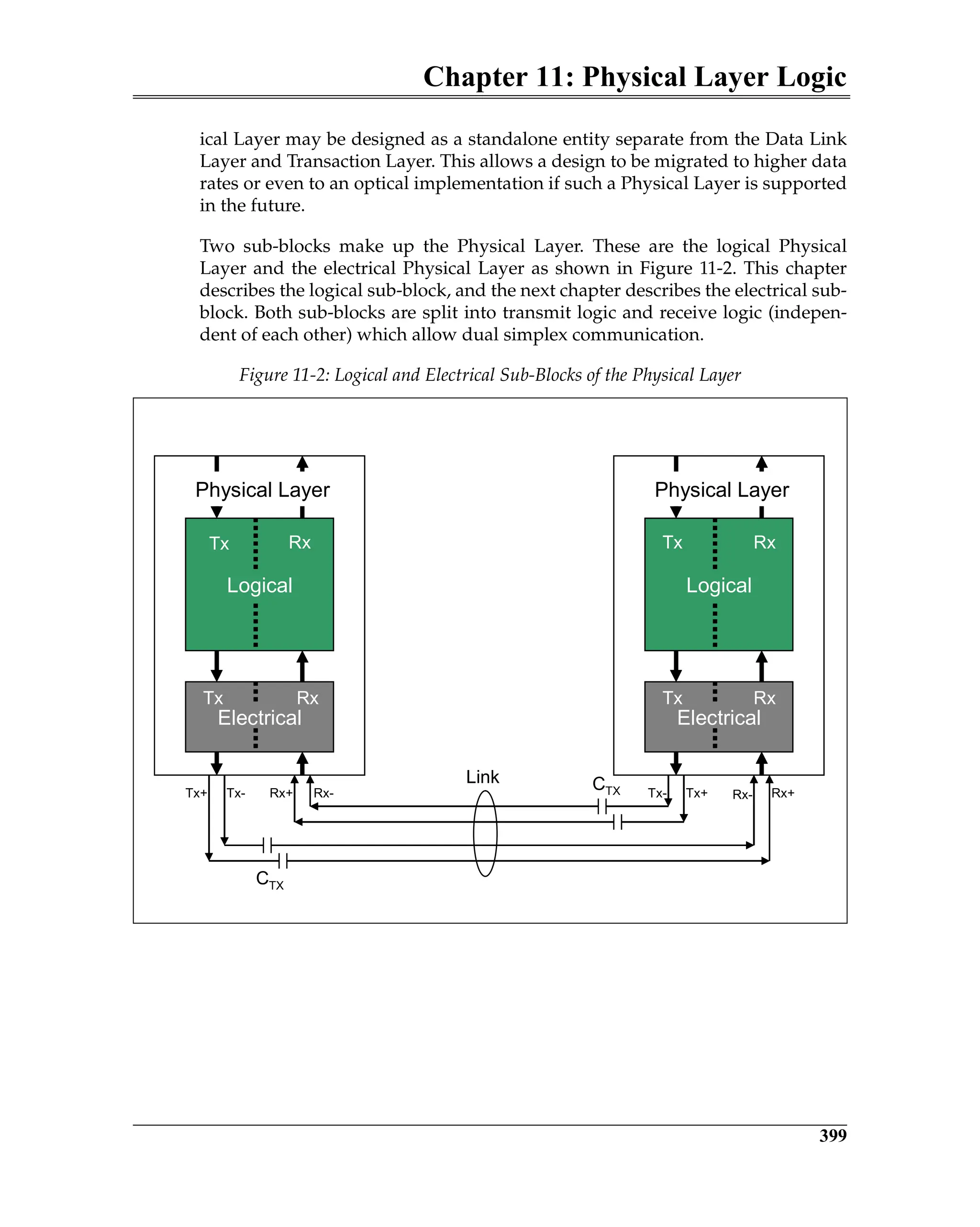
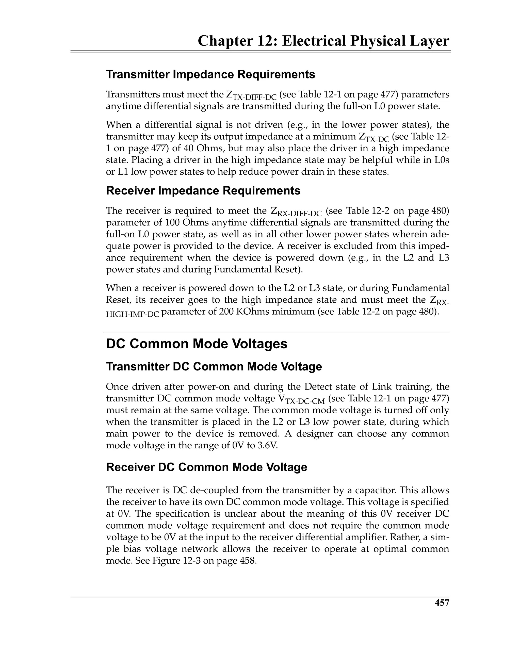
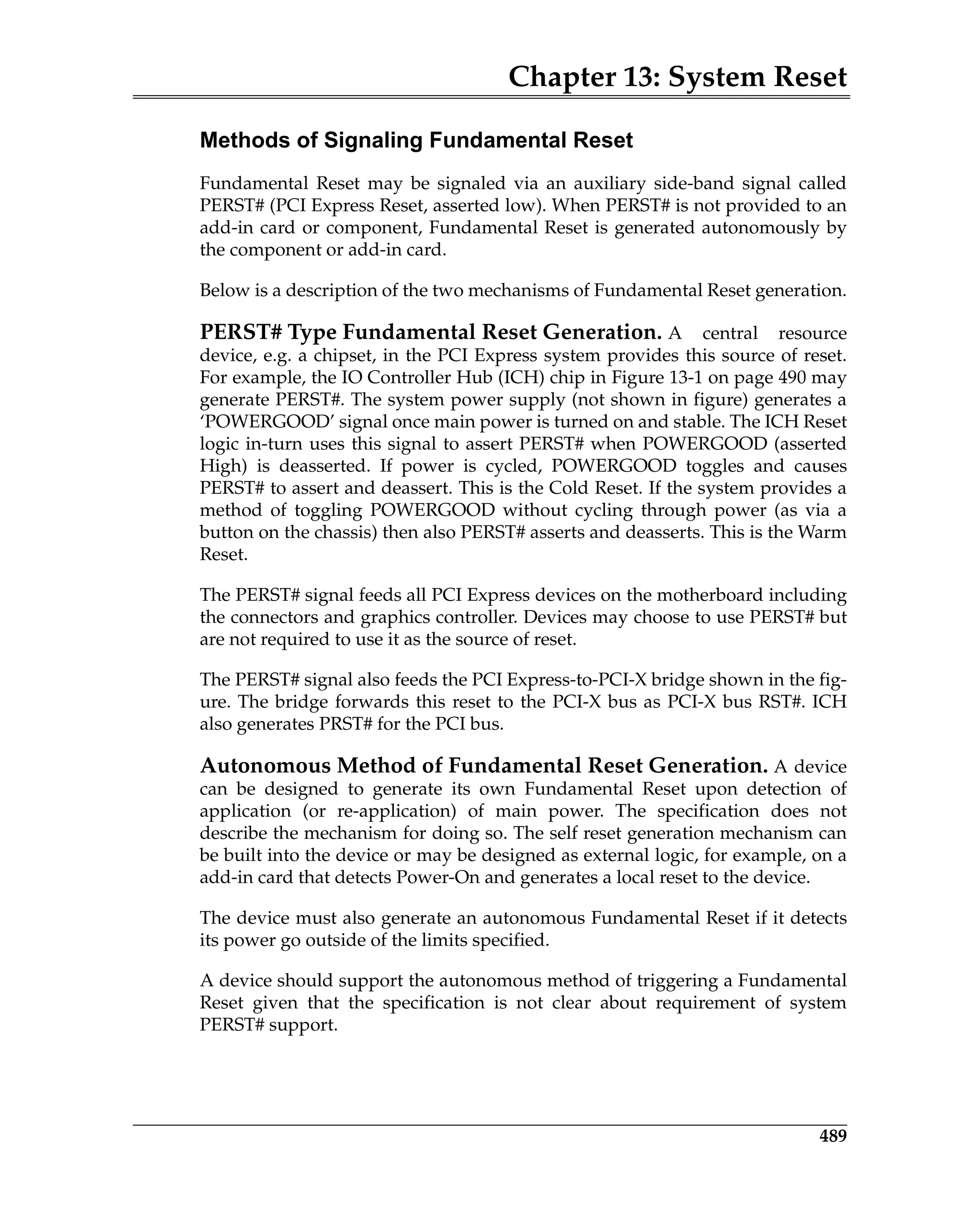
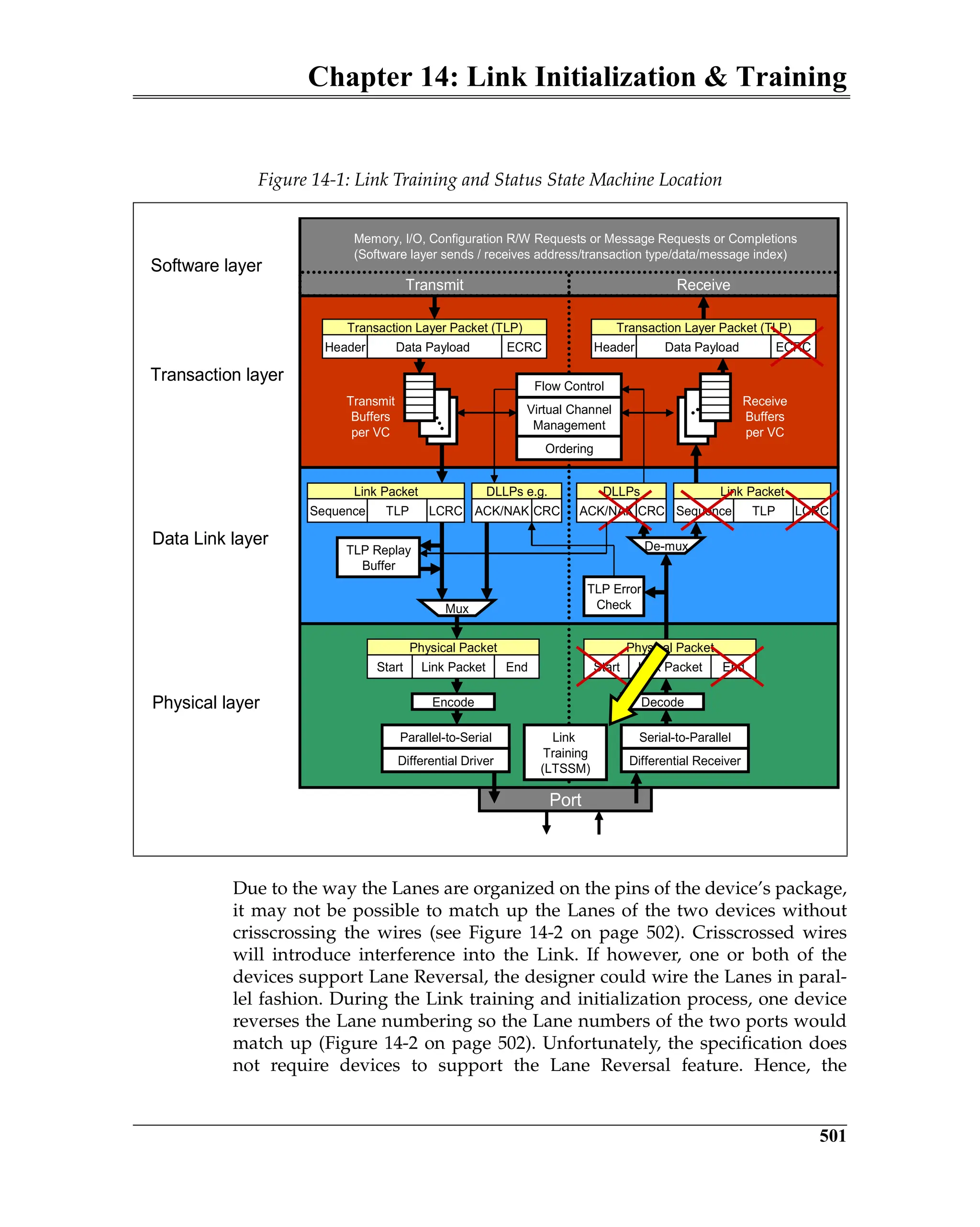
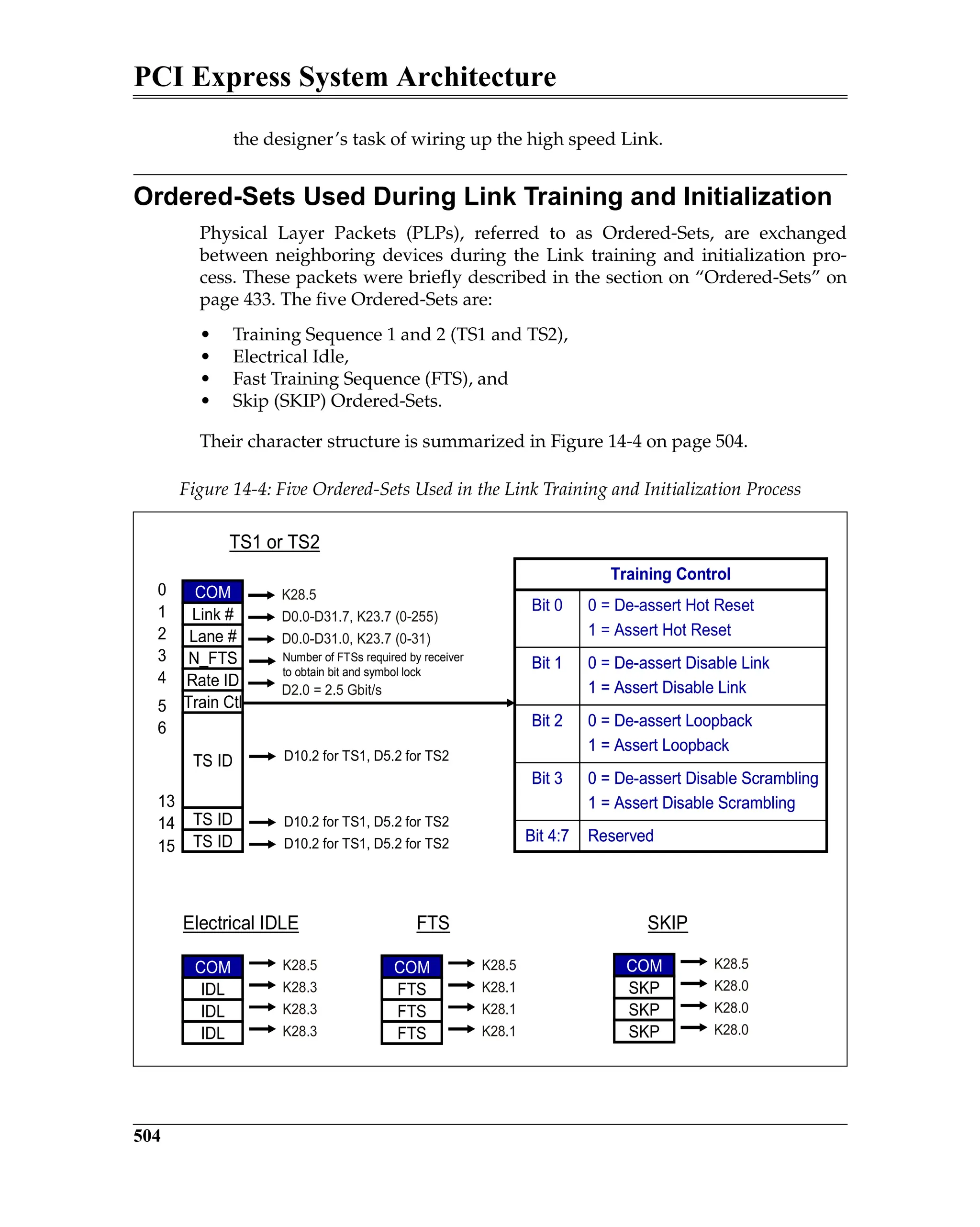
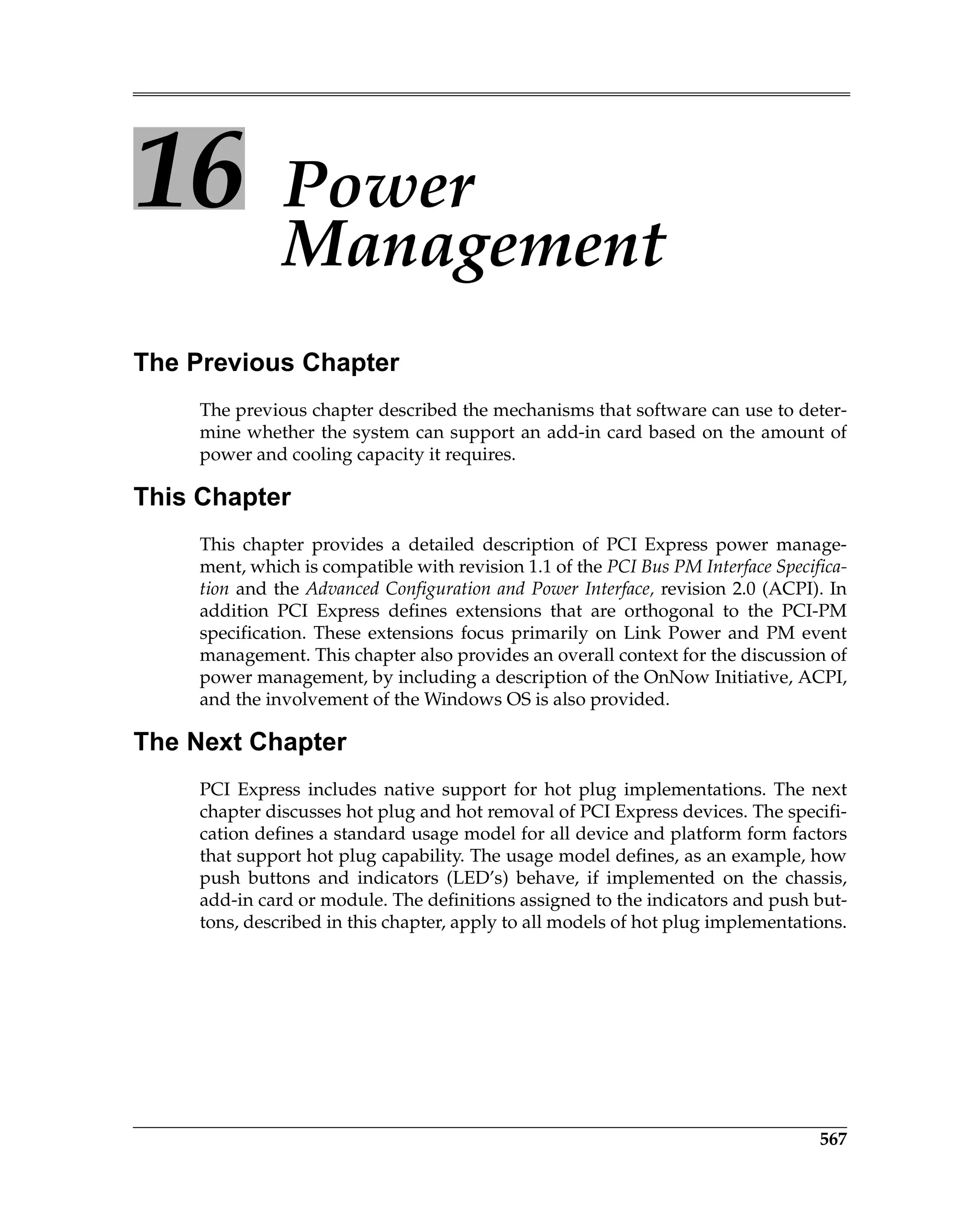
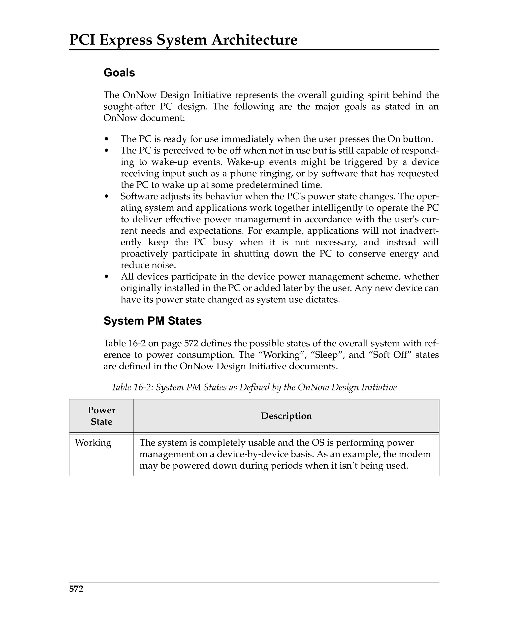
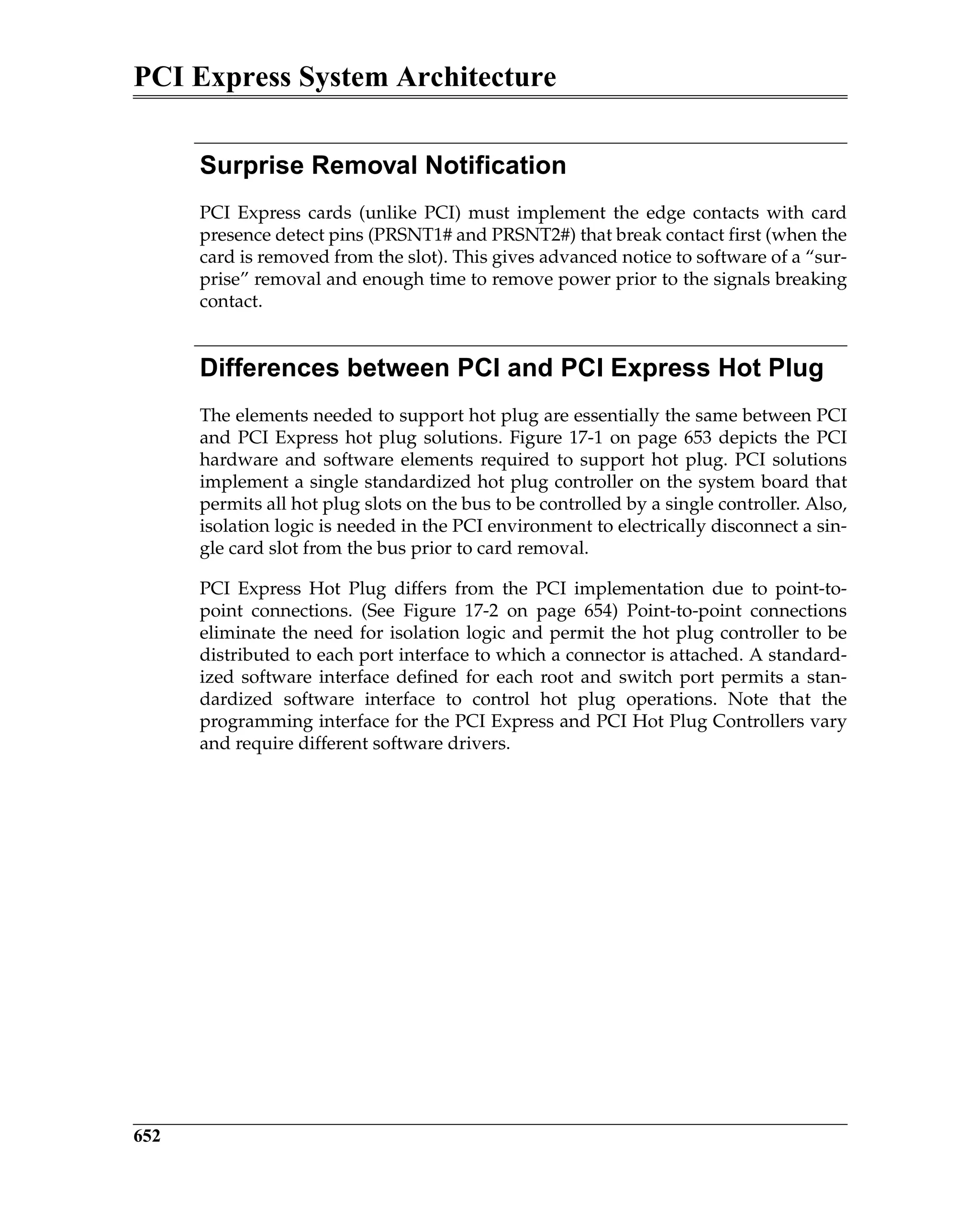
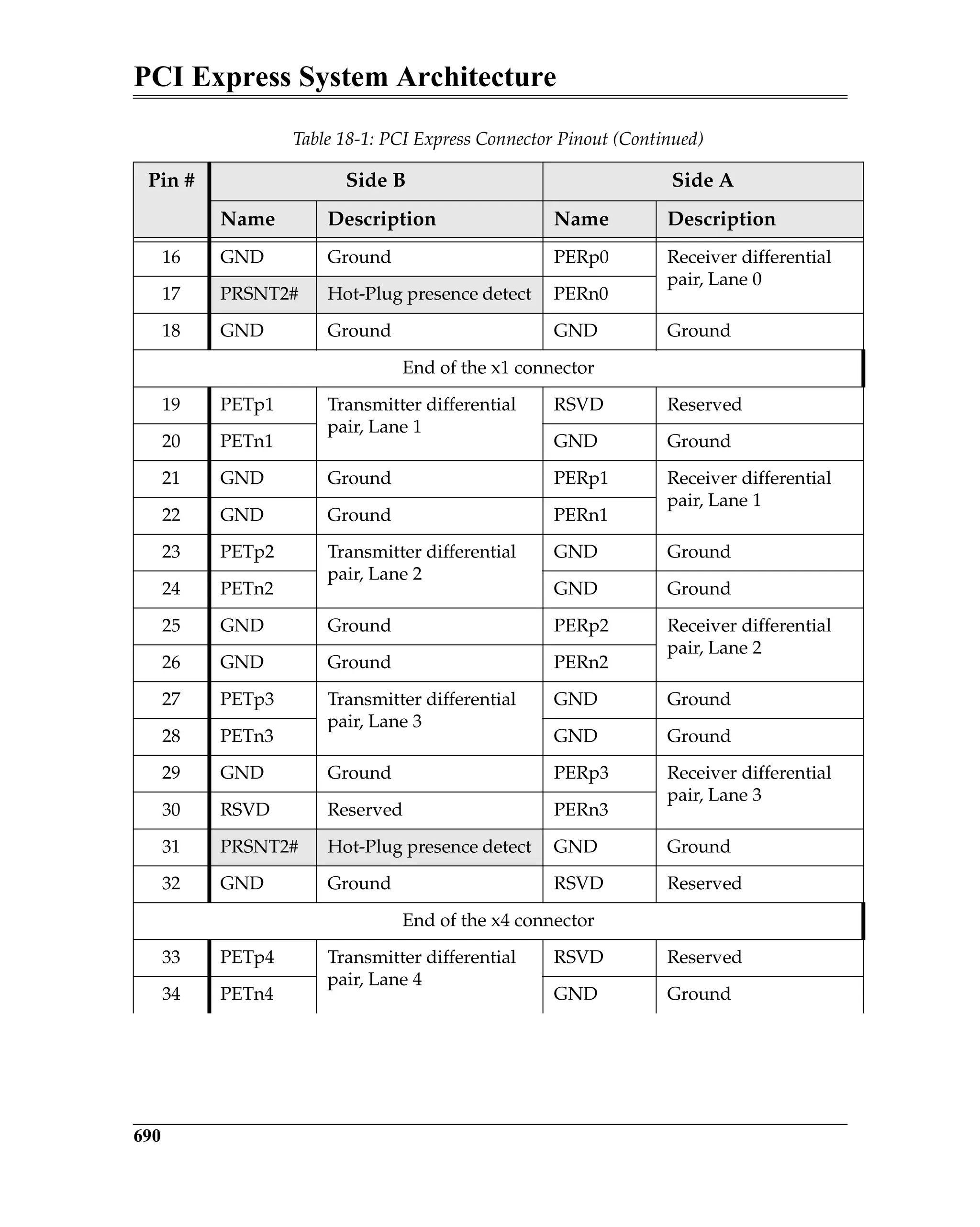
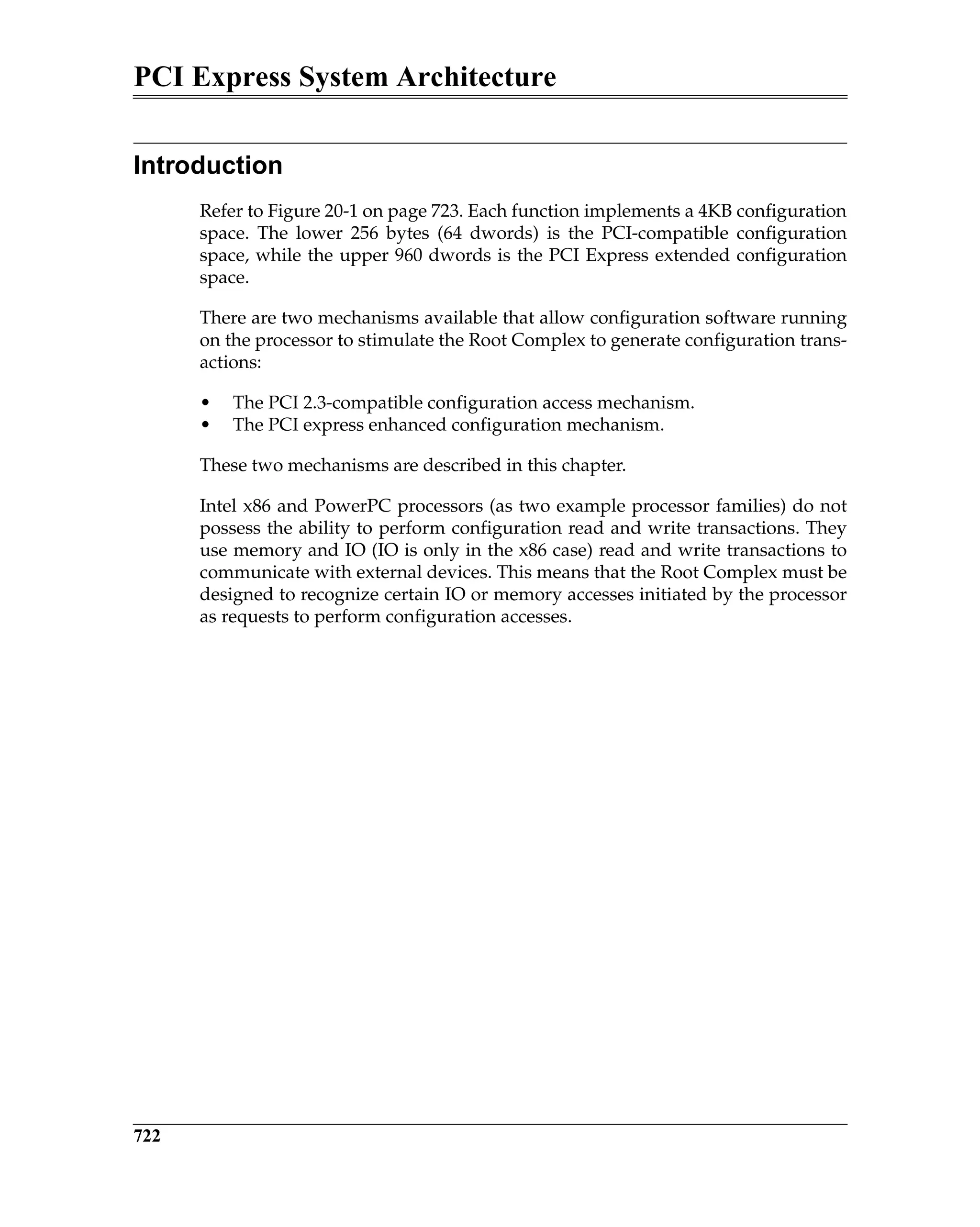
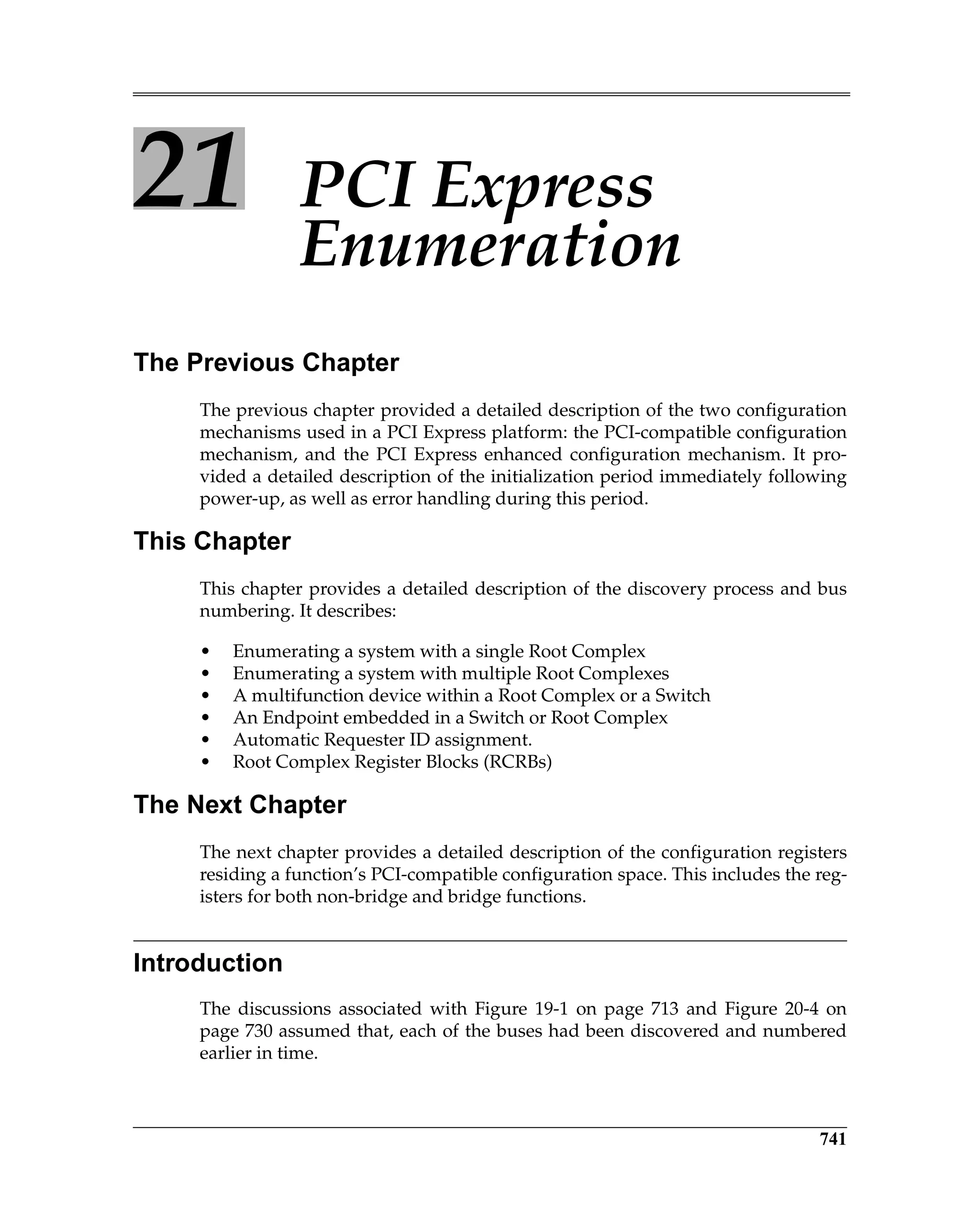
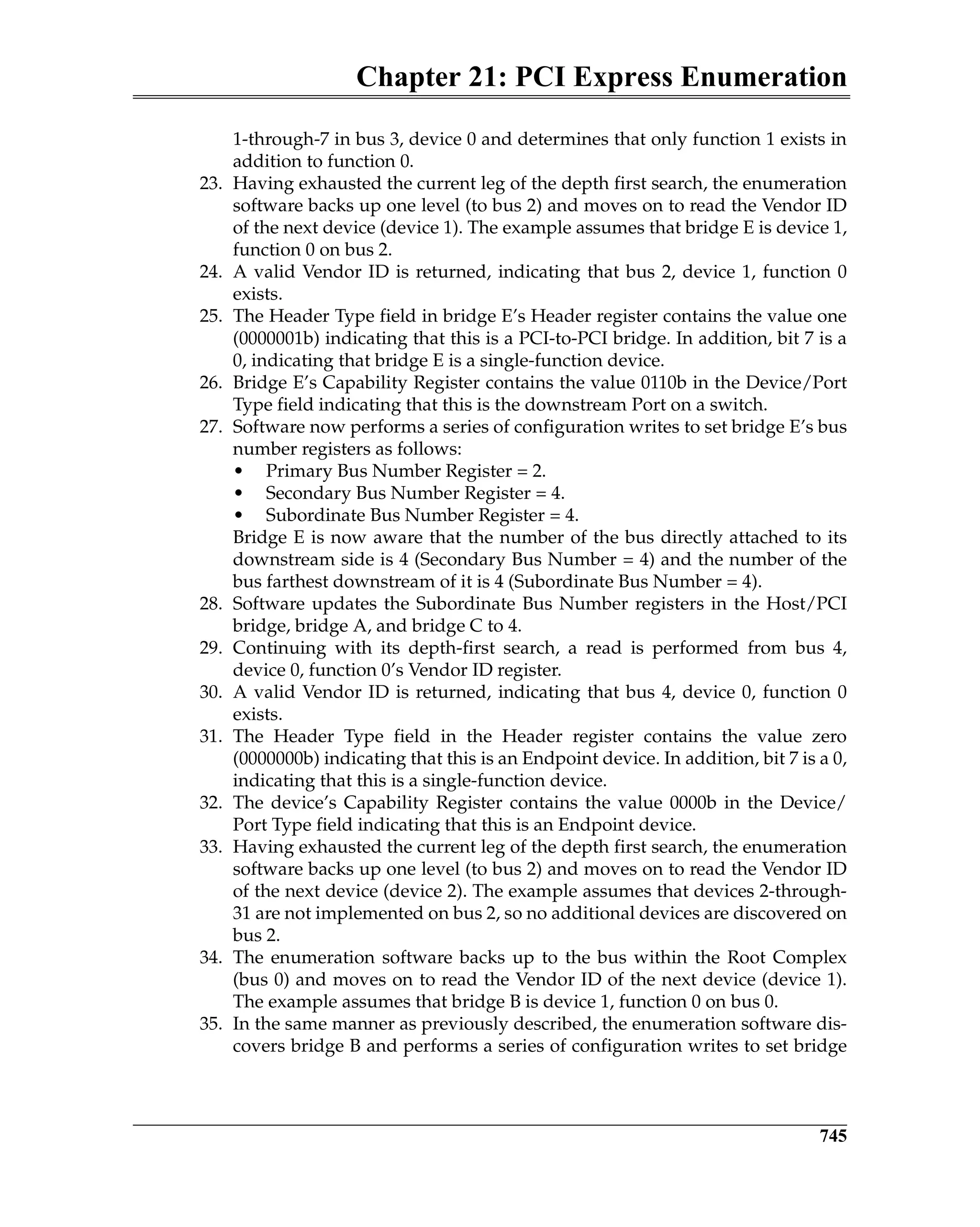
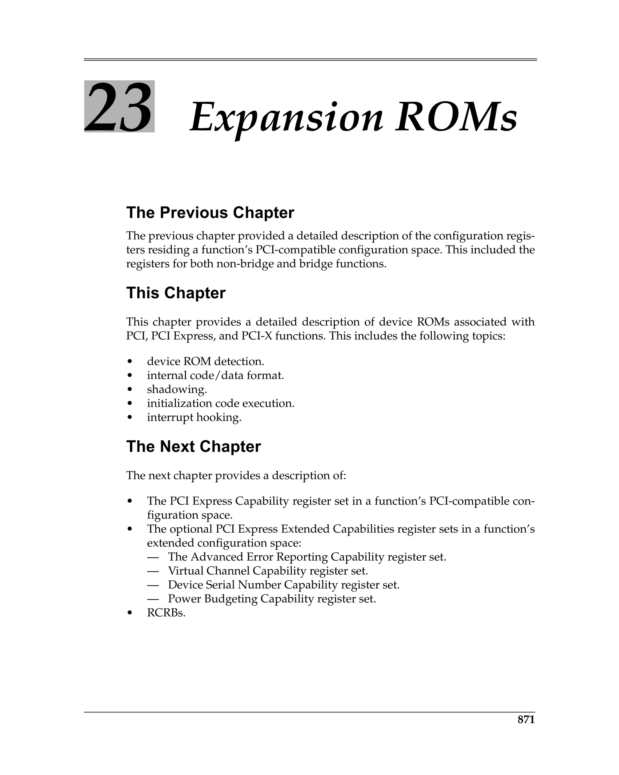
Figure 5-3 is a block diagram of a transmitter and a remote receiver connected
via a Link. The diagram shows all of the major Data Link Layer elements associ-
ated with reliable TLP transfer from the transmitter’s Transaction Layer to the
receiver’s Transaction Layer. Packet order is maintained by the transmitter’s
and receiver’s Transaction Layer.
Figure 5-3: Elements of the ACK/NAK Protocol
Link
Assign
Seq. Num.
NEXT_TRANSMIT_SEQ (NTS)
LCRC Generator
Increment
Replay Buffer
ACK/NAK CRC Check ?
Pass
Fail
Discard
REPLAY_NUM
REPLAY_TIMER
Reset
AckNak_Seq_Num Check
AckNak_Seq_Num =
ACK_SEQ (AS) ?
Block
TLP
during
Replay
DLLP
ACK/NAK
TLP
TLP TLP
ACK/NAK
Generator
Receive Buffer
LCRC Check ?
Seq. Num. Check
TLP Seq. Num (>, <, =)
NEXT_RCV_SEQ (NRS) ?
NEXT_RCV_SEQ (NRS)
Increment
TLP = NRS
NAK_SCHEDULED
Pass
Fail
NAK
TLP > NRS (Lost TLPs)
Schedule
ACK
TLP < NRS (Duplicate TLP)
TLPs
ACKNAK_LAT
_TIMER
Schedule
NAK
AckNak_Seq_Num[11:0]
From Transaction Layer
Transmitter Device A
To Transaction Layer
Receiver Device B
(NTS-AS) mod 4k >= 2048 ?
Yes - Block TLP, report DL
Layer protocol error
Good TLPs
Update ACK_SEQ (AS)
No (Forward Progress)
Purge Older TLPs
NAK
?
Yes
Yes
Replay
NAK
Increment](https://image.slidesharecdn.com/pciexpresssystemarchitecture-240110064541-2f1f00b9/75/pci-express-system-architecture-pdf-75-2048.jpg)
![PCI Express System Architecture
214
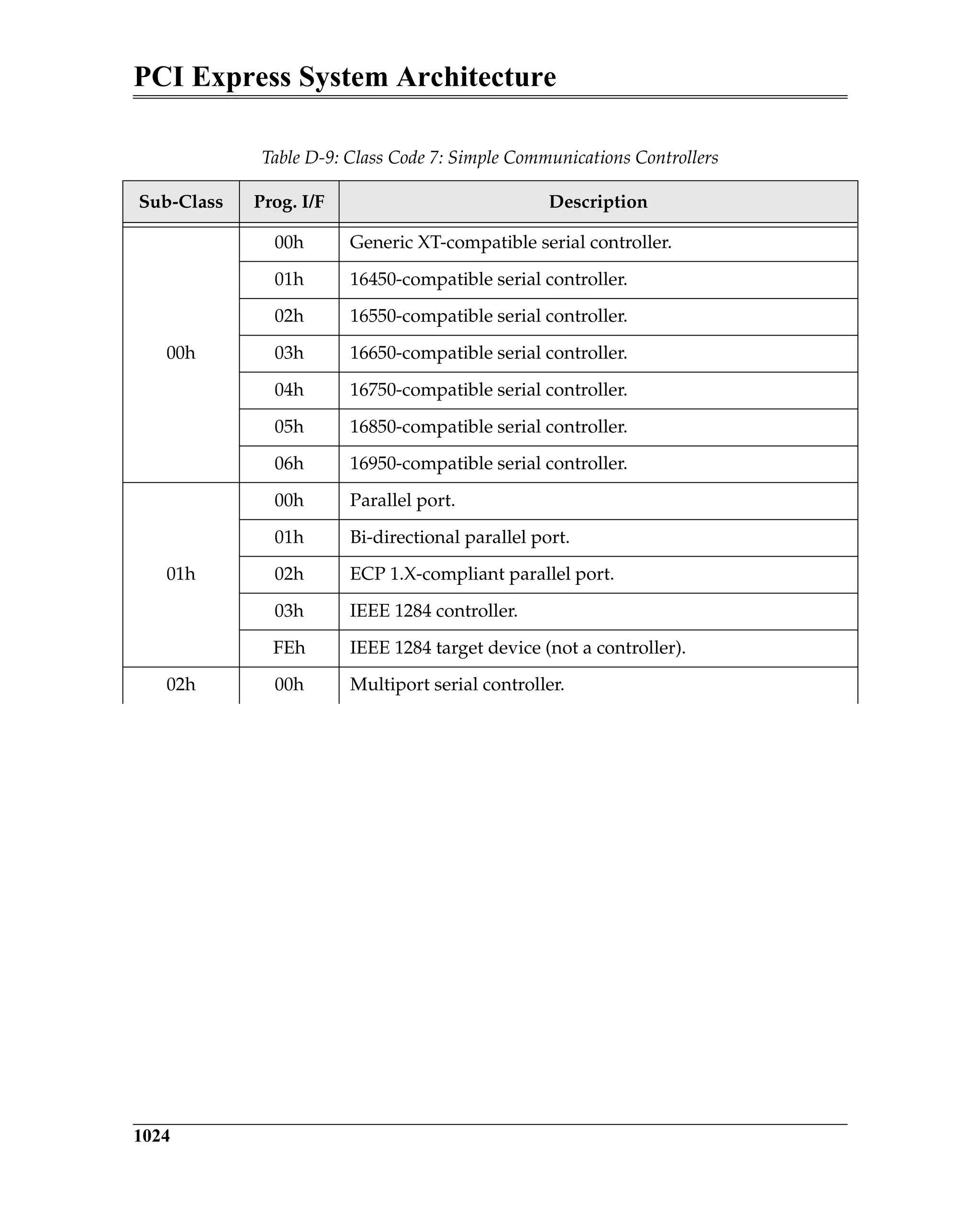
REPLAY_TIMER Count
The REPLAY_TIMER is used to measure the time from when a TLP is transmit-
ted until an associated ACK or NAK DLLP is received. The REPLAY_TIMER is
started (or restarted, if already running) when the last Symbol of any TLP is
sent. It restarts from 0 each time that there are outstanding TLPs in the Replay
Buffer and an ACK DLLP is received that references a TLP still in the Replay
Buffer. It resets to 0 and holds when there are no outstanding TLPs in the Replay
Buffer, or until restart conditions are met for each NAK received (except during
a replay), or when the REPLAY_TIMER expires. It is not advanced (i.e., its value
remains fixed) during Link re-training.
ACKD_SEQ Count
This 12-bit register tracks or stores the Sequence Number of the most recently
received ACK or NAK DLLP. It is initialized to all 1s at reset, or when the Data
Link Layer is inactive. This register is updated with the AckNak_Seq_Num
[11:0] field of a received ACK or NAK DLLP. The ACKD_SEQ count is com-
pared with the NEXT_TRANSMIT_SEQ count.
IF (NEXT_TRANSMIT_SEQ - ACKD_SEQ) mod 4096 ≥ 2048 THEN
New TLPs from Transaction Layer are not accepted by Data Link Layer until
this equation is no longer true. In addition, a Data Link Layer protocol error
which is a fatal uncorrectable error is reported. This error condition occurs if
there is a separation greater than 2047 between NEXT_TRANSMIT_SEQ and
ACKD_SEQ. i.e, a separation greater than 2047 between the sequence number
of a TLP being transmitted and that of a TLP in the replay buffer that receives an
ACK or NAK DLLP.
Also, the ACKD_SEQ count is used to check for forward progress made in
transmitting TLPs. If no forward progress is made after 3 additional replay
attempts, the Link in re-trained.
DLLP CRC Check
This block checks for CRC errors in DLLPs returned from the receiver. Good
DLLPs are further processed. If a DLLP CRC error is detected, the DLLP is dis-
carded and an error reported. No further action is taken.
Definition: The Data Link Layer is in the inactive state when the Physical Layer
reports that the Link is non-operational or nothing is connected to the Port. The
Physical Layer is in the non-operational state when the Link Training and Status
State Machine (LTSSM) is in the Detect, Polling, Configuration, Disabled, Reset](https://image.slidesharecdn.com/pciexpresssystemarchitecture-240110064541-2f1f00b9/75/pci-express-system-architecture-pdf-77-2048.jpg)


![Chapter 20: Configuration Mechanisms
725
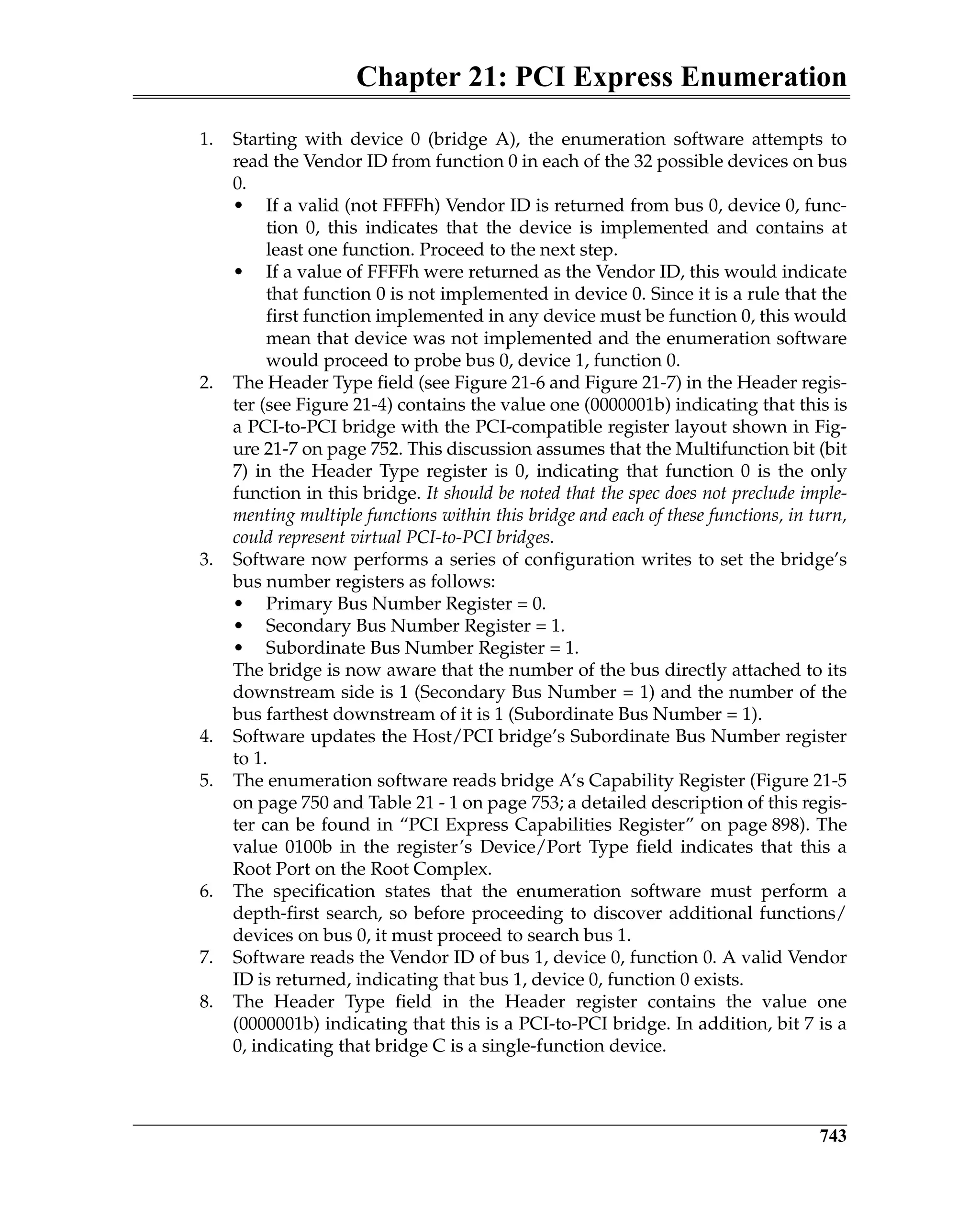
Accessing one of a function's PCI-compatible configuration registers is a two
step process:
1. Write the target bus number, device number, function number and dword
number to the Configuration Address Port and set the Enable bit in it to
one.
2. Perform a one-byte, two-byte, or four-byte IO read from or a write to the
Configuration Data Port.
In response, the host/PCI bridge within the Root Complex compares the speci-
fied target bus to the range of buses that exist on the other side of the bridge
and, if the target bus resides beyond the bridge, it initiates a configuration read
or write transaction (based on whether the processor is performing an IO read
or write with the Configuration Data Port).
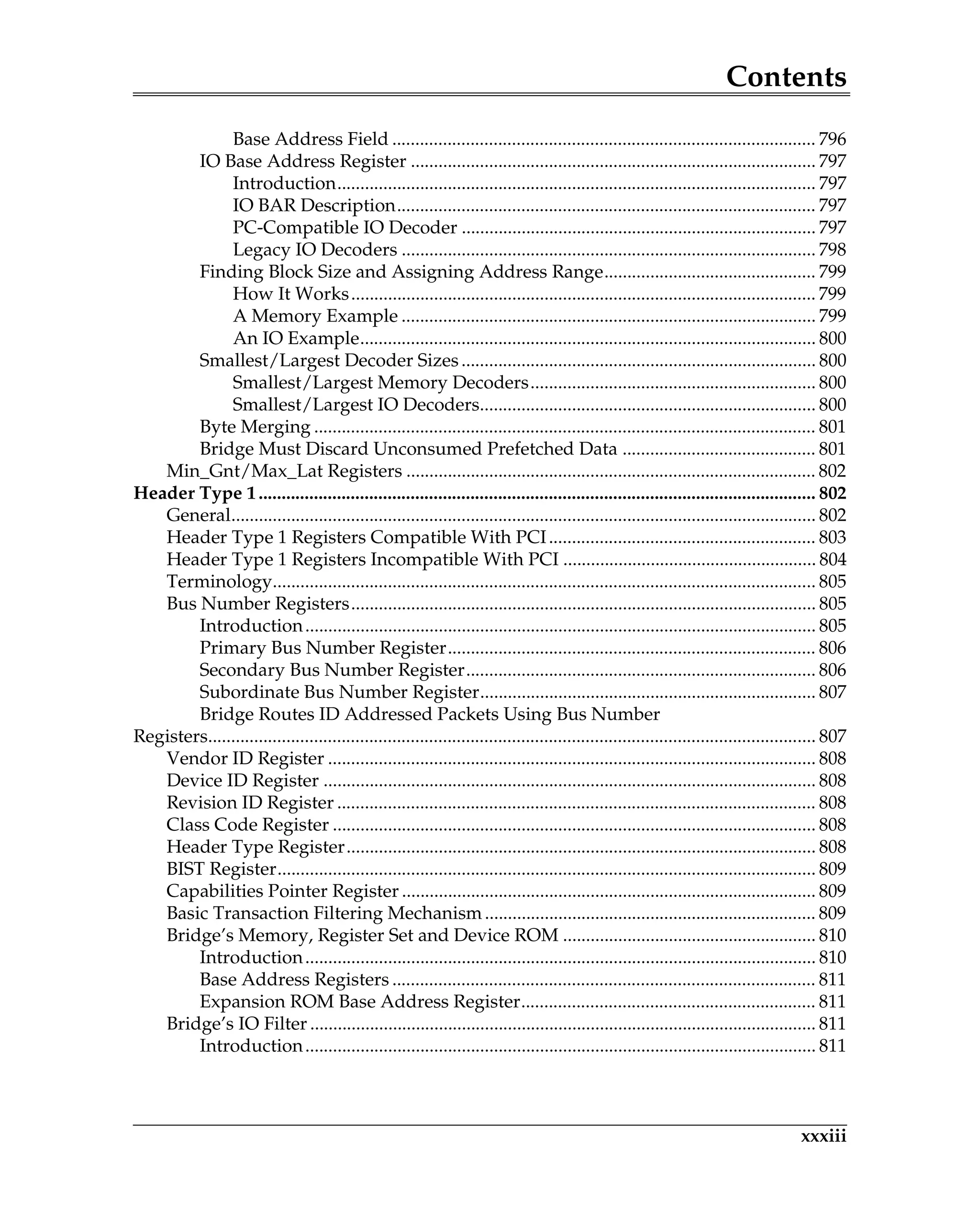
Configuration Address Port
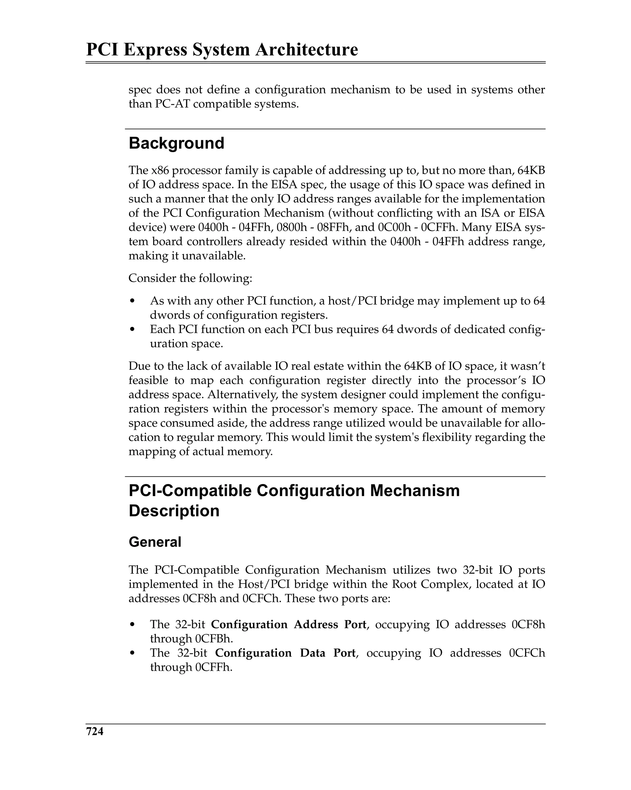
Refer to Figure 20-2 on page 726. The Configuration Address Port only latches
information when the processor performs a full 32-bit write to the port. A 32-bit
read from the port returns its contents. The assertion of reset clears the port to
all zeros. Any 8- or 16-bit access within this IO dword is treated as an 8- or 16-bit
IO access. The 32-bits of information written to the Configuration Address Port
must conform to the following template (illustrated in Figure 20-2 on page 726):
• bits [1:0] are hard-wired, read-only and must return zeros when read.
• bits [7:2] identify the target dword (1-of-64) within the target function's PCI-
compatible configuration space. When the Root Complex subsequently
generates the resultant configuration request packet, this bit field supplies
the content of the packet’s Register Number field and the packet’s Extended
Register Number field is set to all zeros. This configuration access mecha-
nism is therefore limited to addressing the first 64 dwords of the targeted
function’s configuration space (i.e., the function’s PCI-compatible address
space).
• bits [10:8] identify the target function number (1-of-8) within the target
device.
• bits [15:11] identify the target device number (1-of-32).
• bits [23:16] identifies the target bus number (1-of-256).
• bits [30:24] are reserved and must be zero.
• bit 31 must be set to a one, enabling the translation of a subsequent proces-
sor IO access to the Configuration Data Port into a configuration access. If
bit 31 is zero and the processor initiates an IO read from or IO write to the
Configuration Data Port, the transaction is treated as an IO transaction
request.](https://image.slidesharecdn.com/pciexpresssystemarchitecture-240110064541-2f1f00b9/75/pci-express-system-architecture-pdf-166-2048.jpg)
![Chapter 23: Expansion ROMs
873
• assigning a base address to the register’s Base Address field,
• enabling its decoder (by setting bit 0 in the register to one),
• and then attempting to read the first two locations from the ROM.
If the first two locations contain the ROM signature—AA55h—then the ROM is
present.
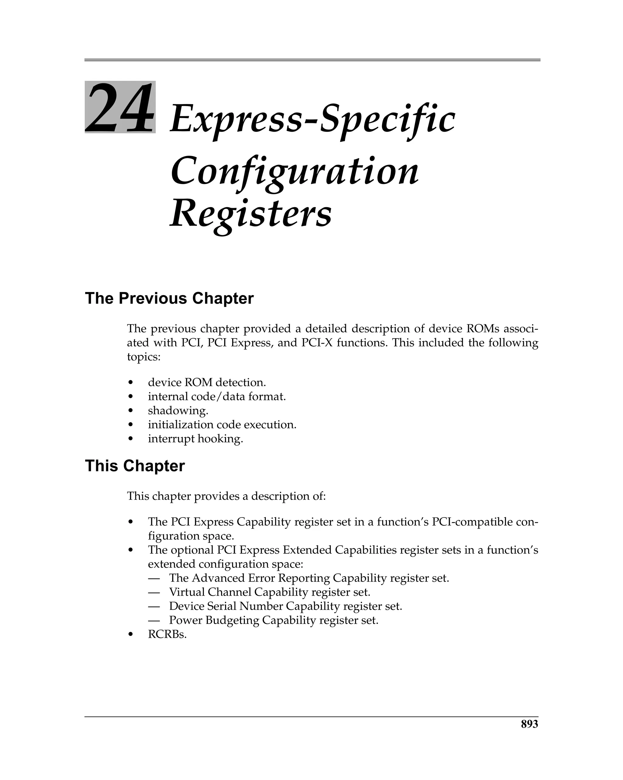
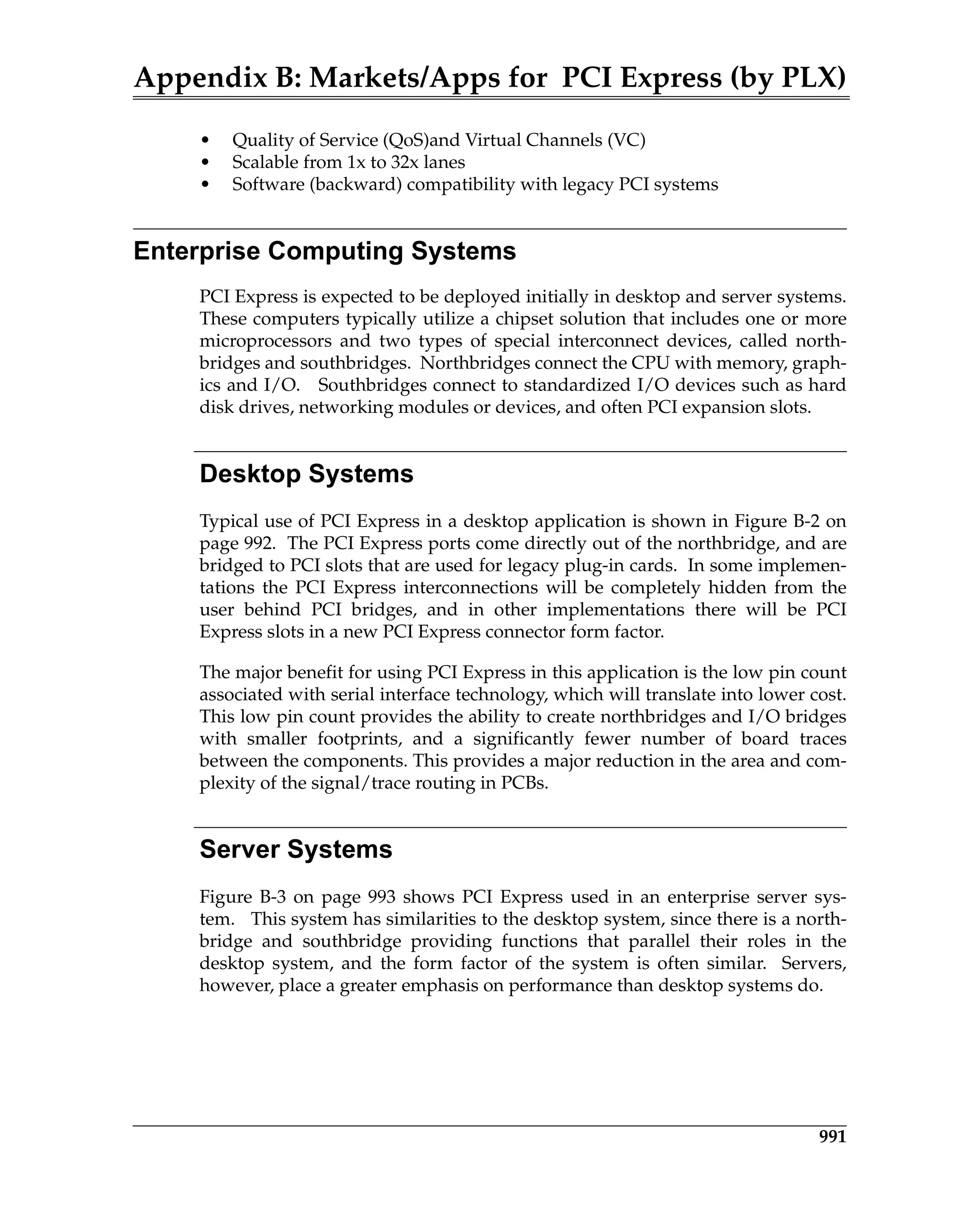
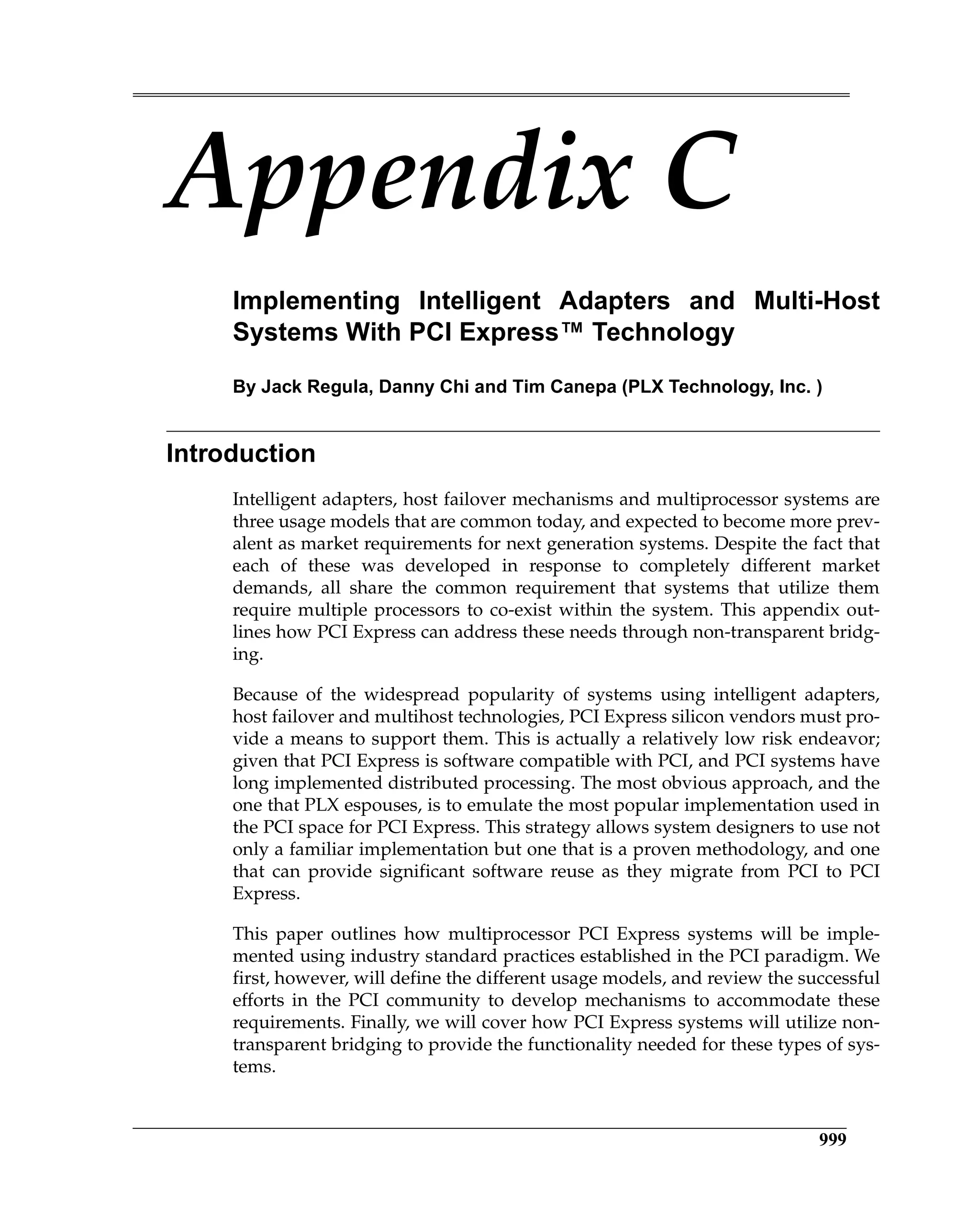
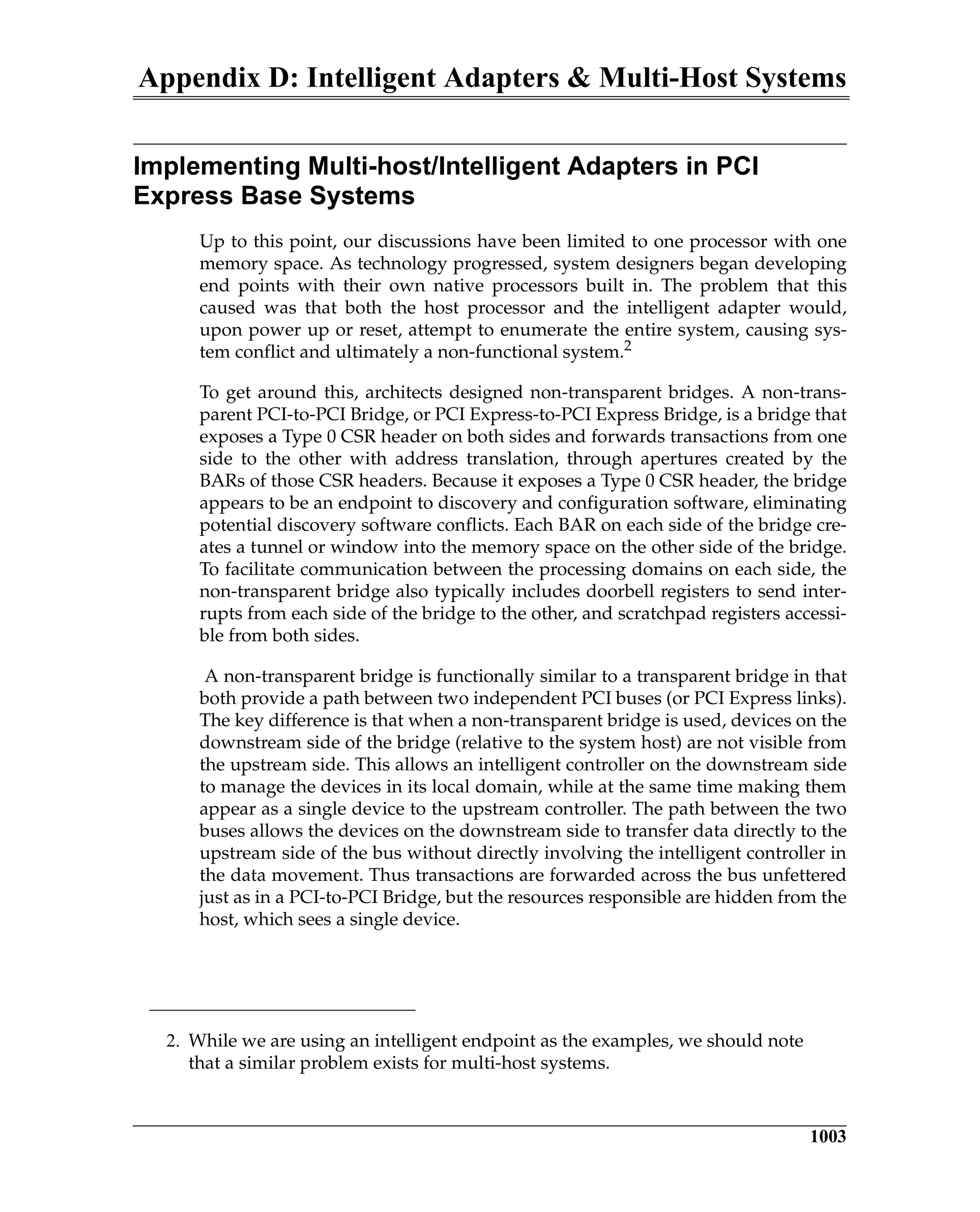
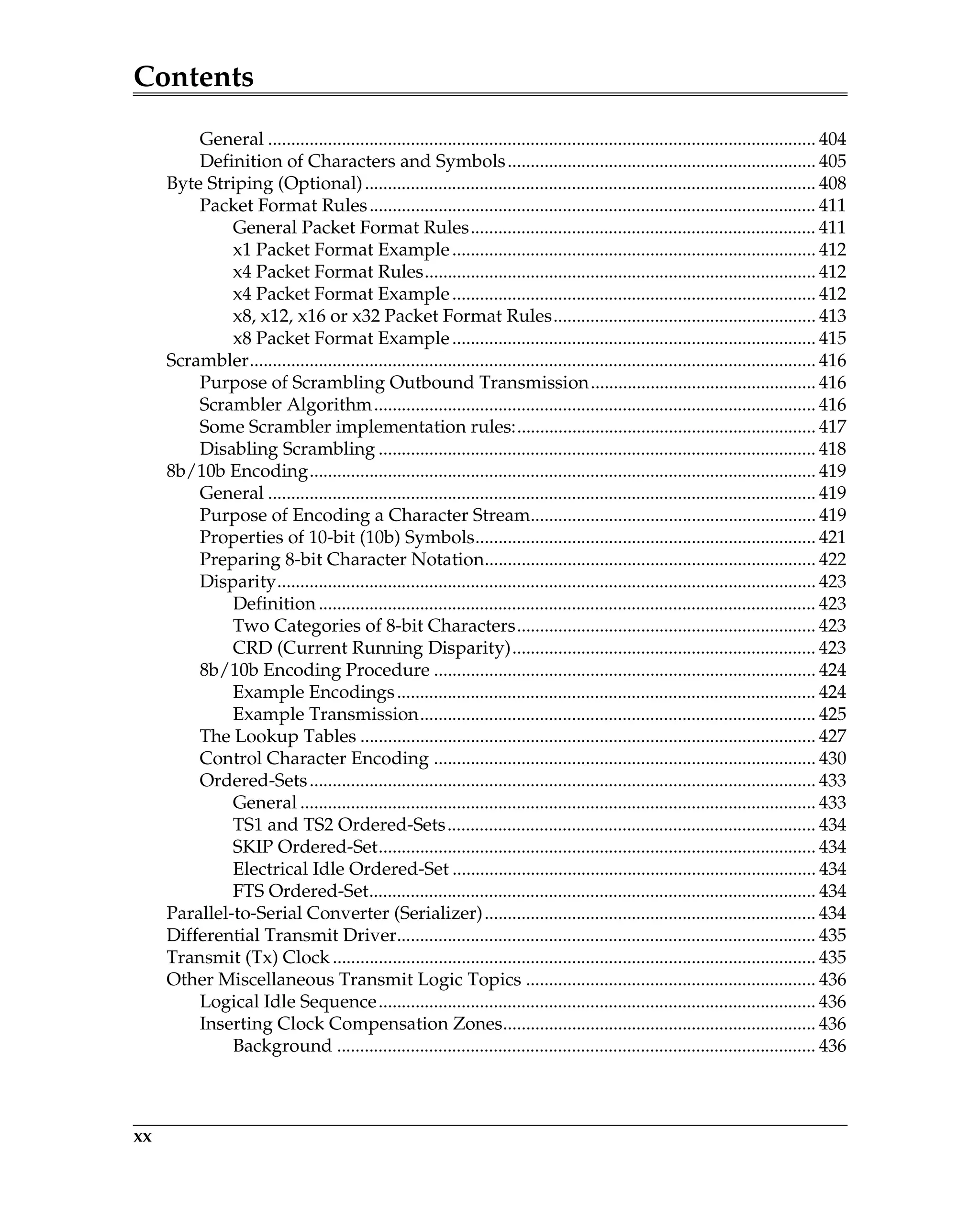
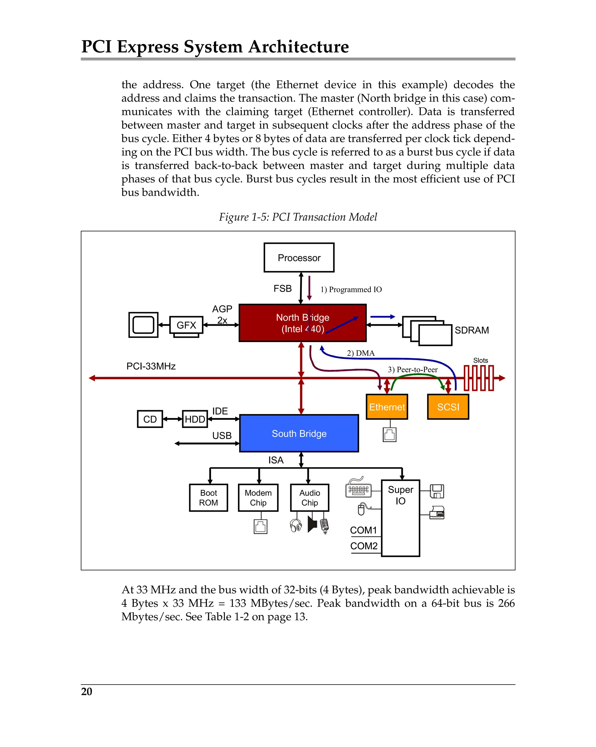
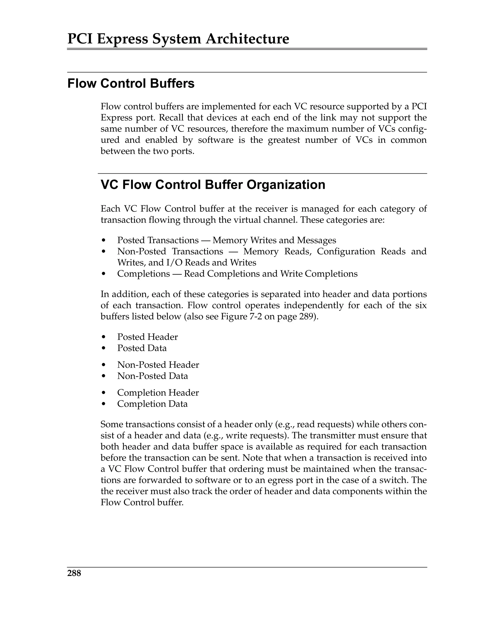
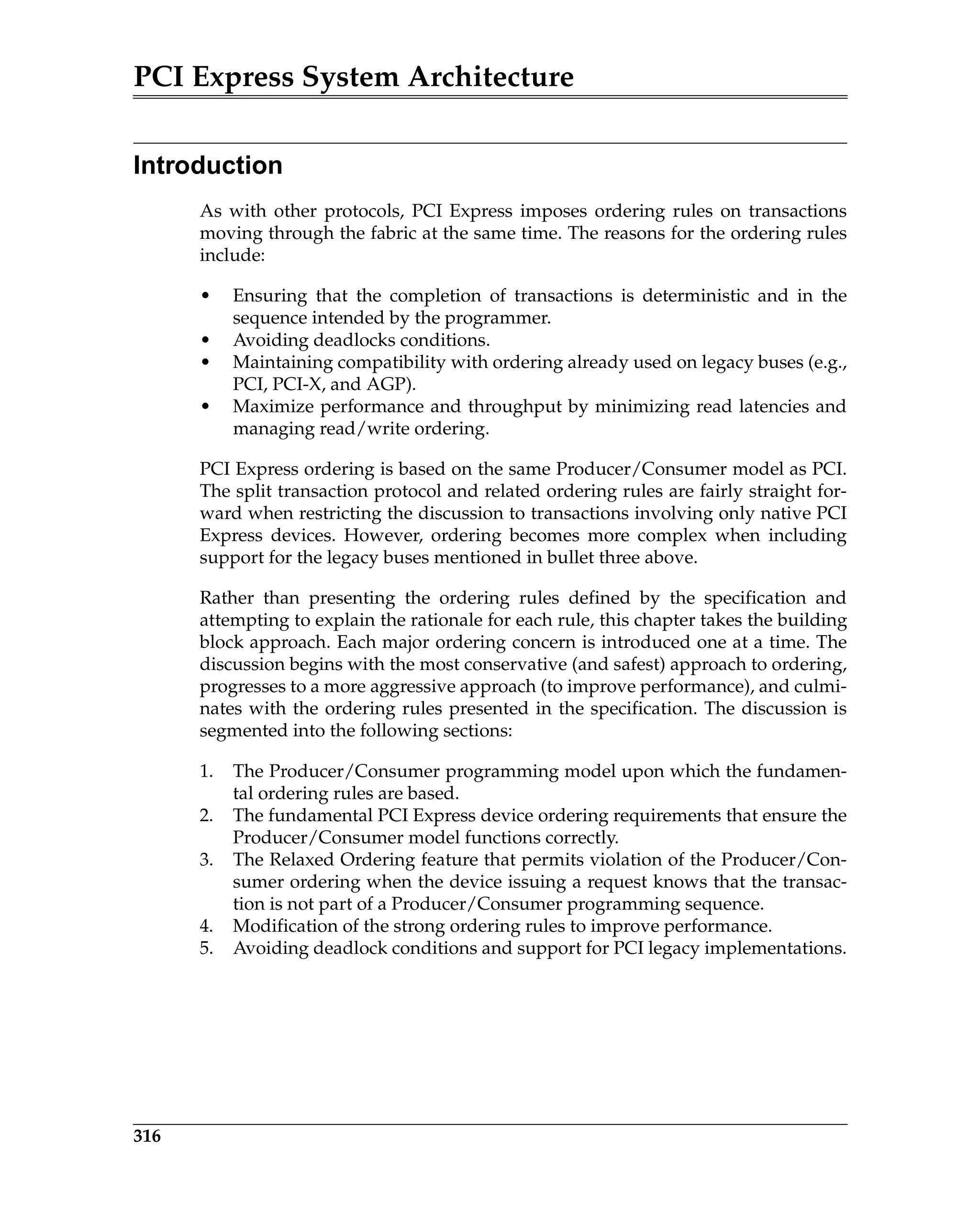
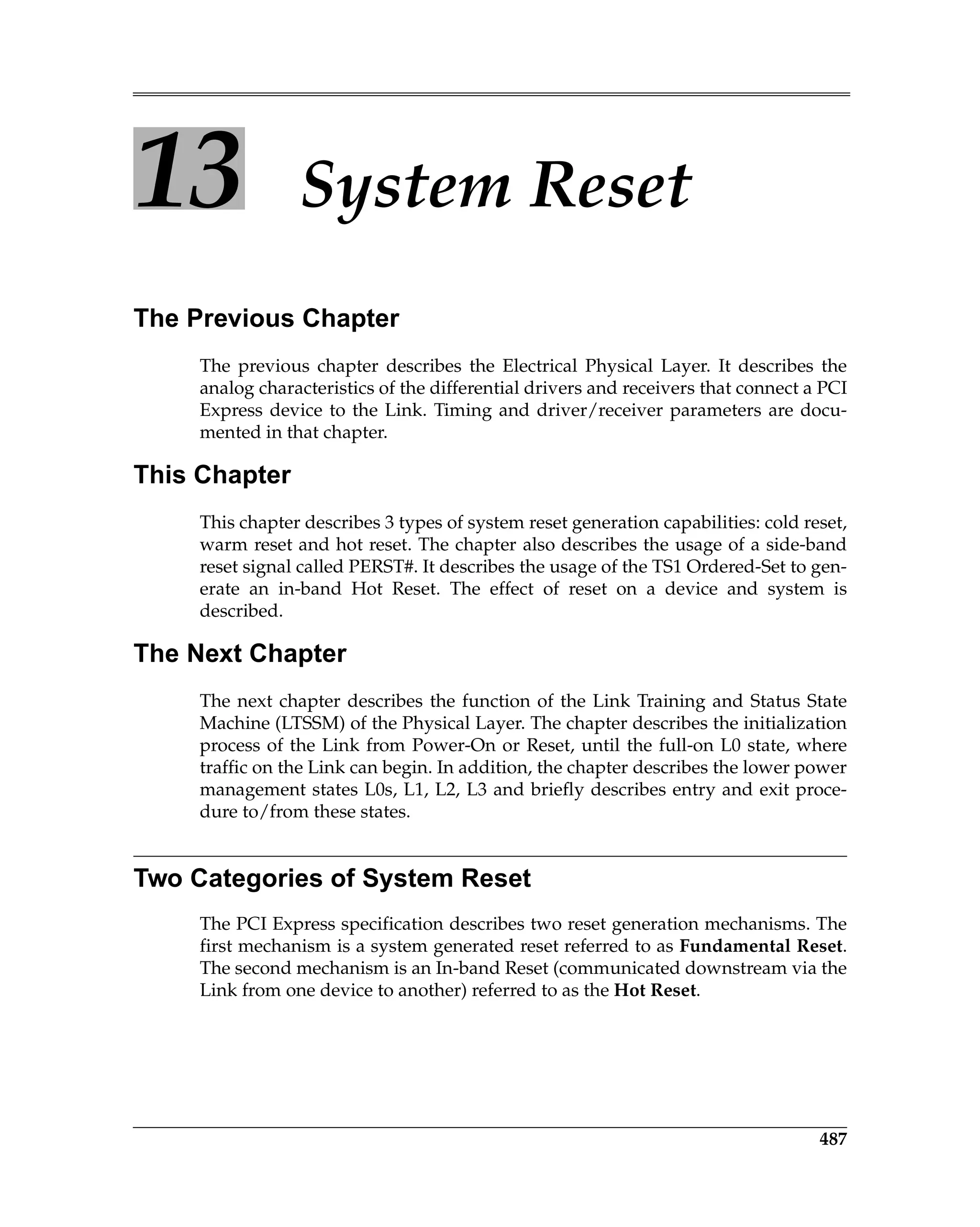
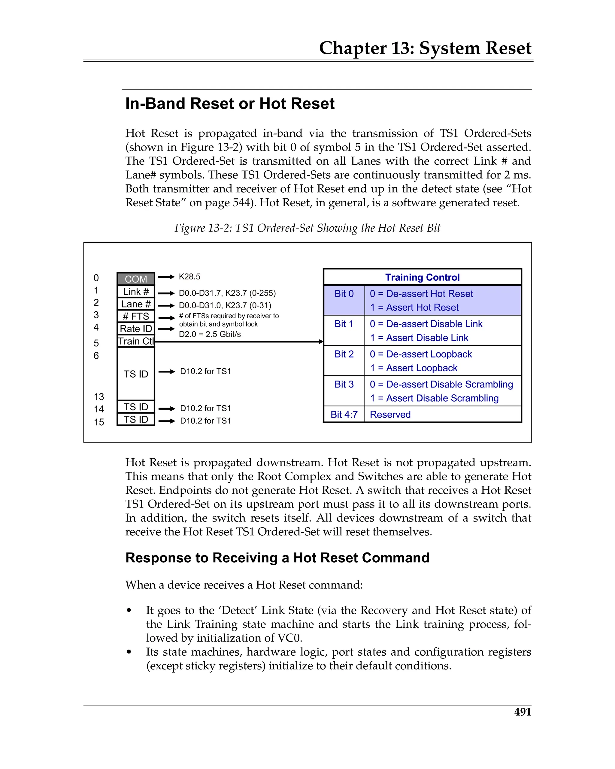
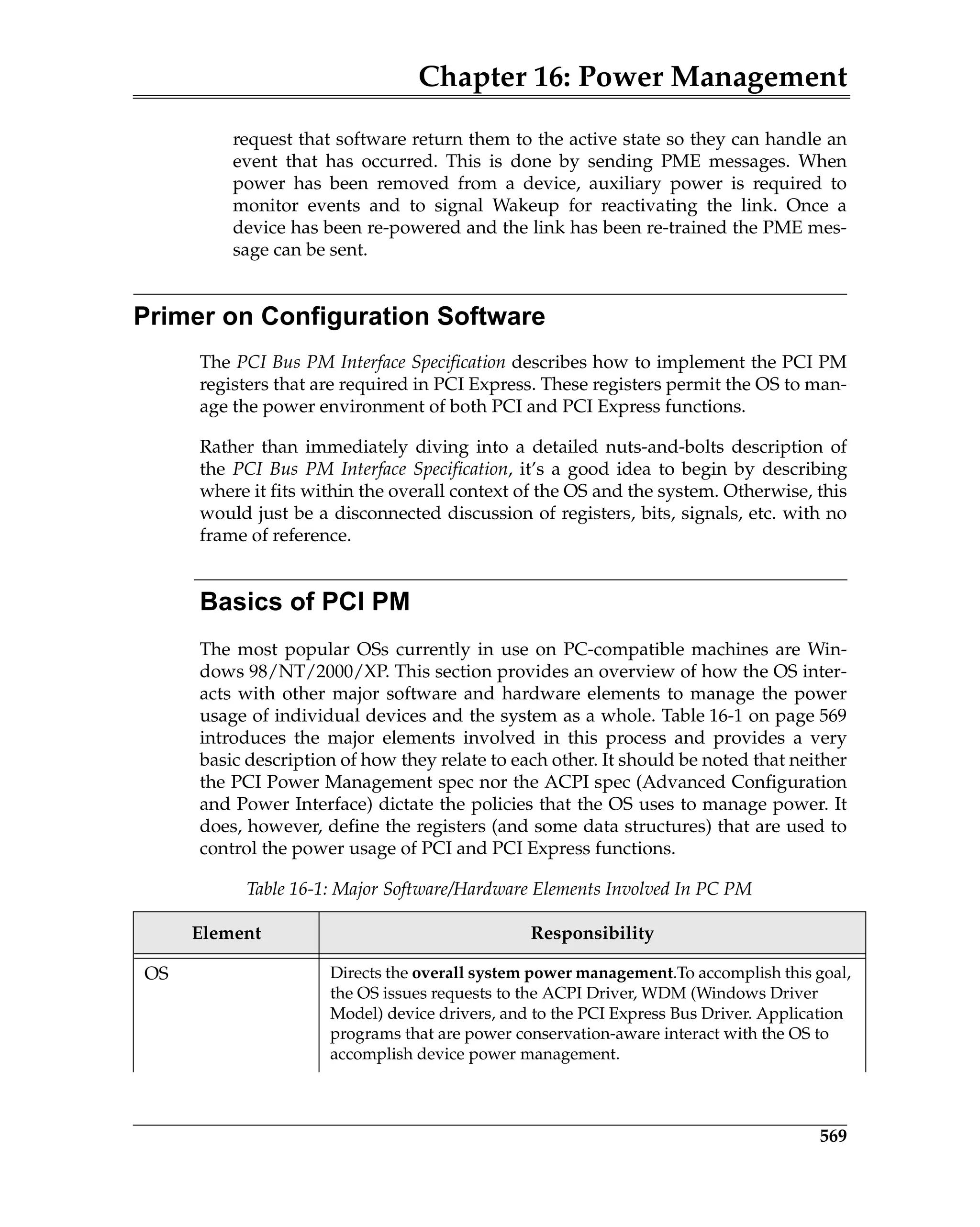
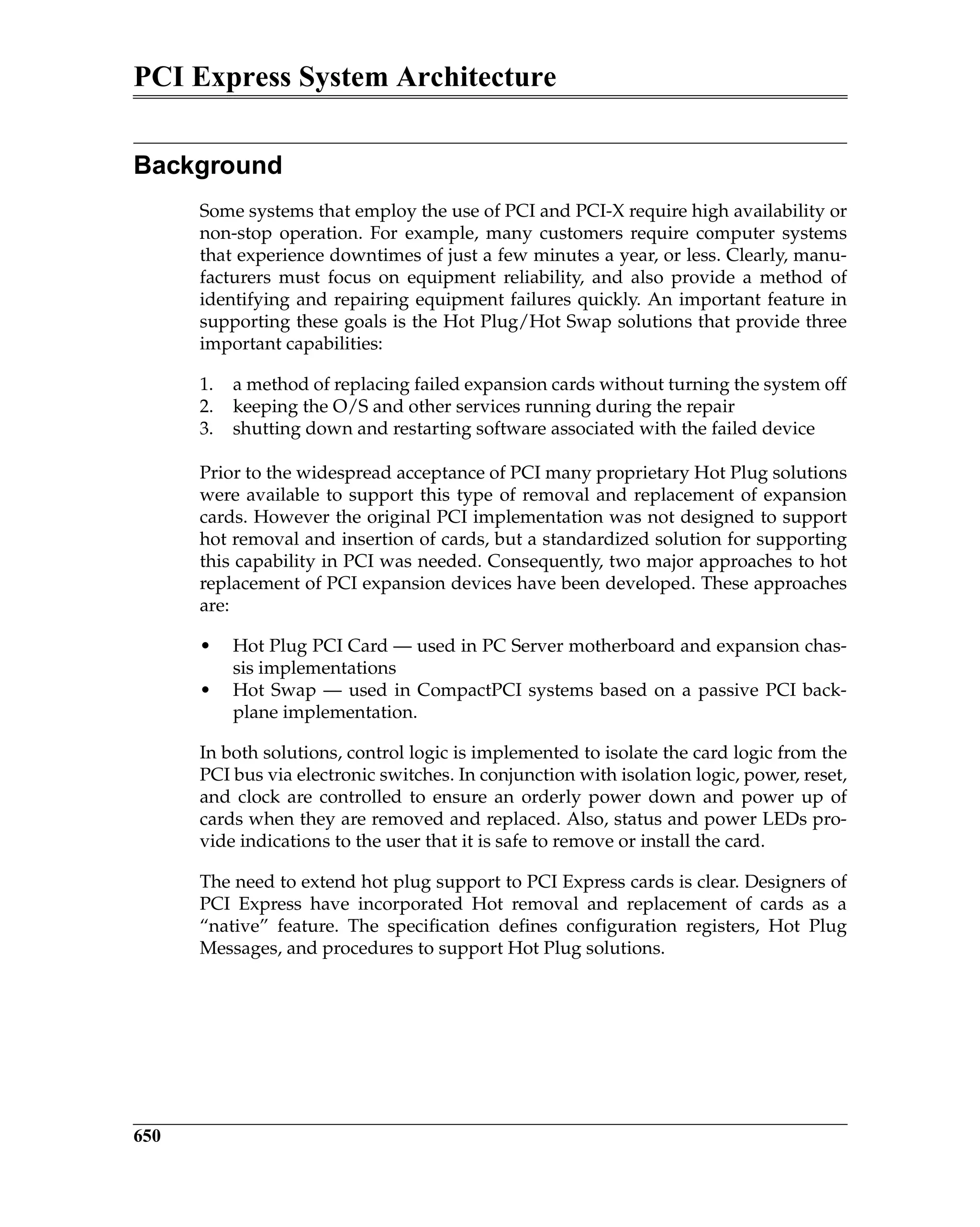
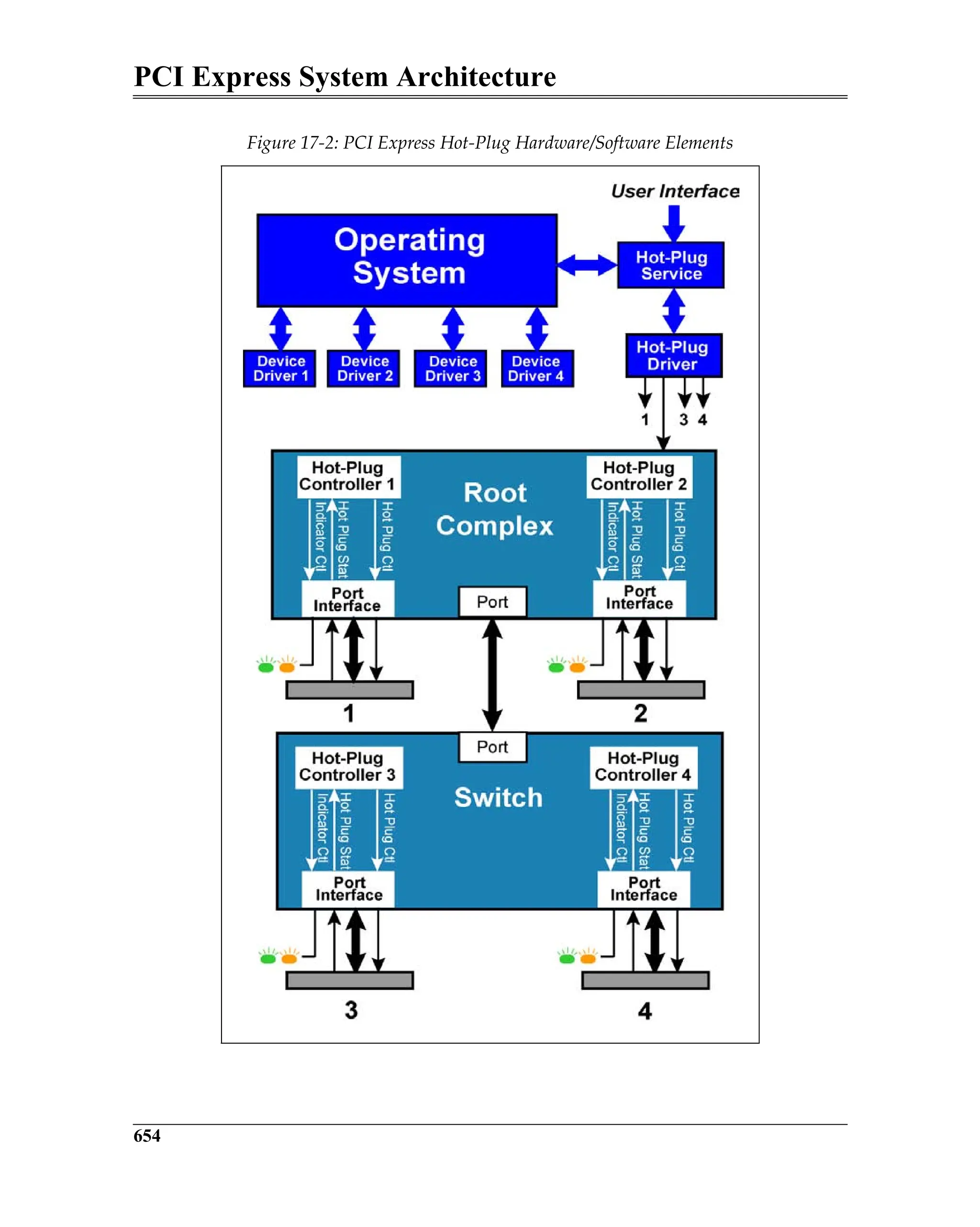
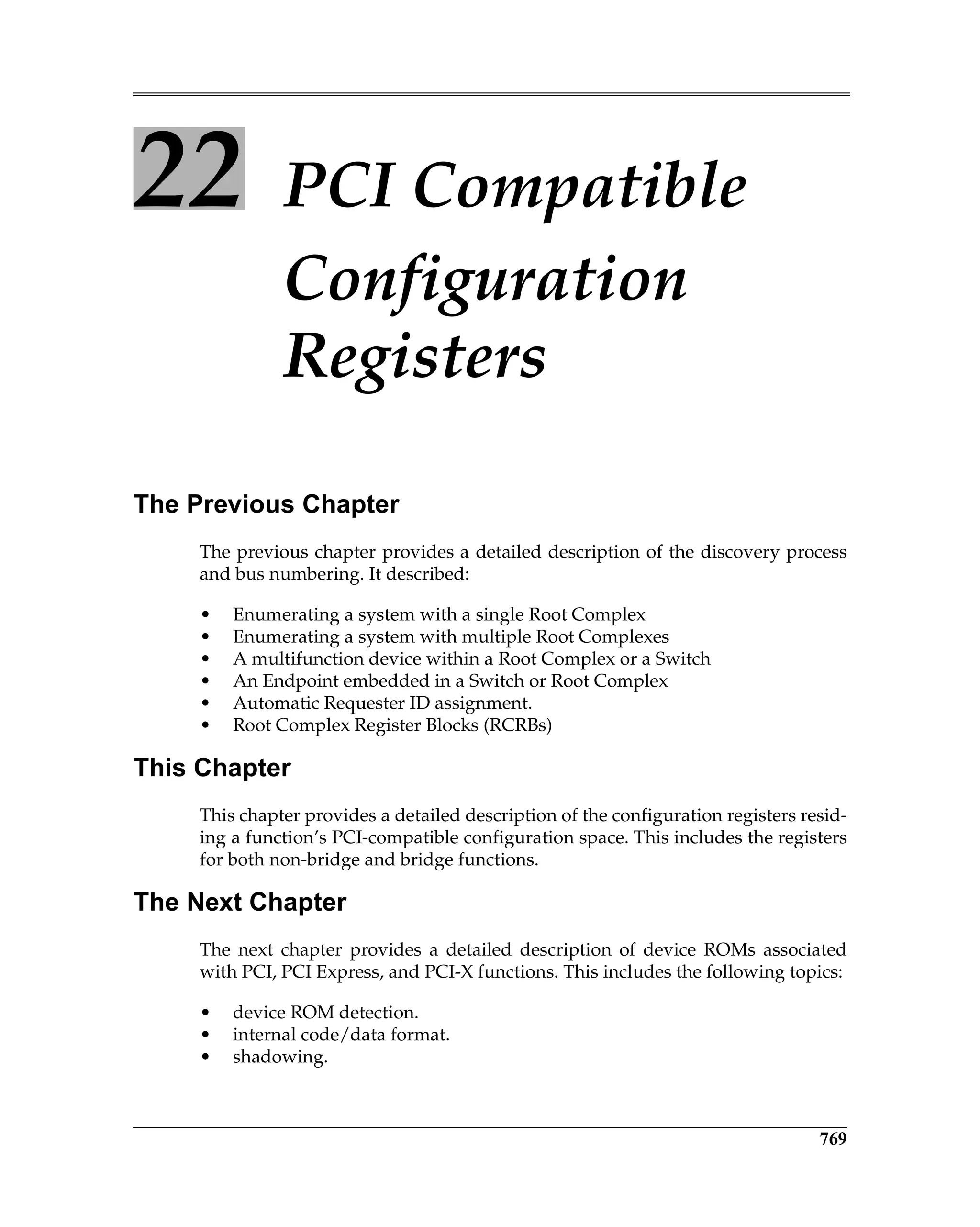
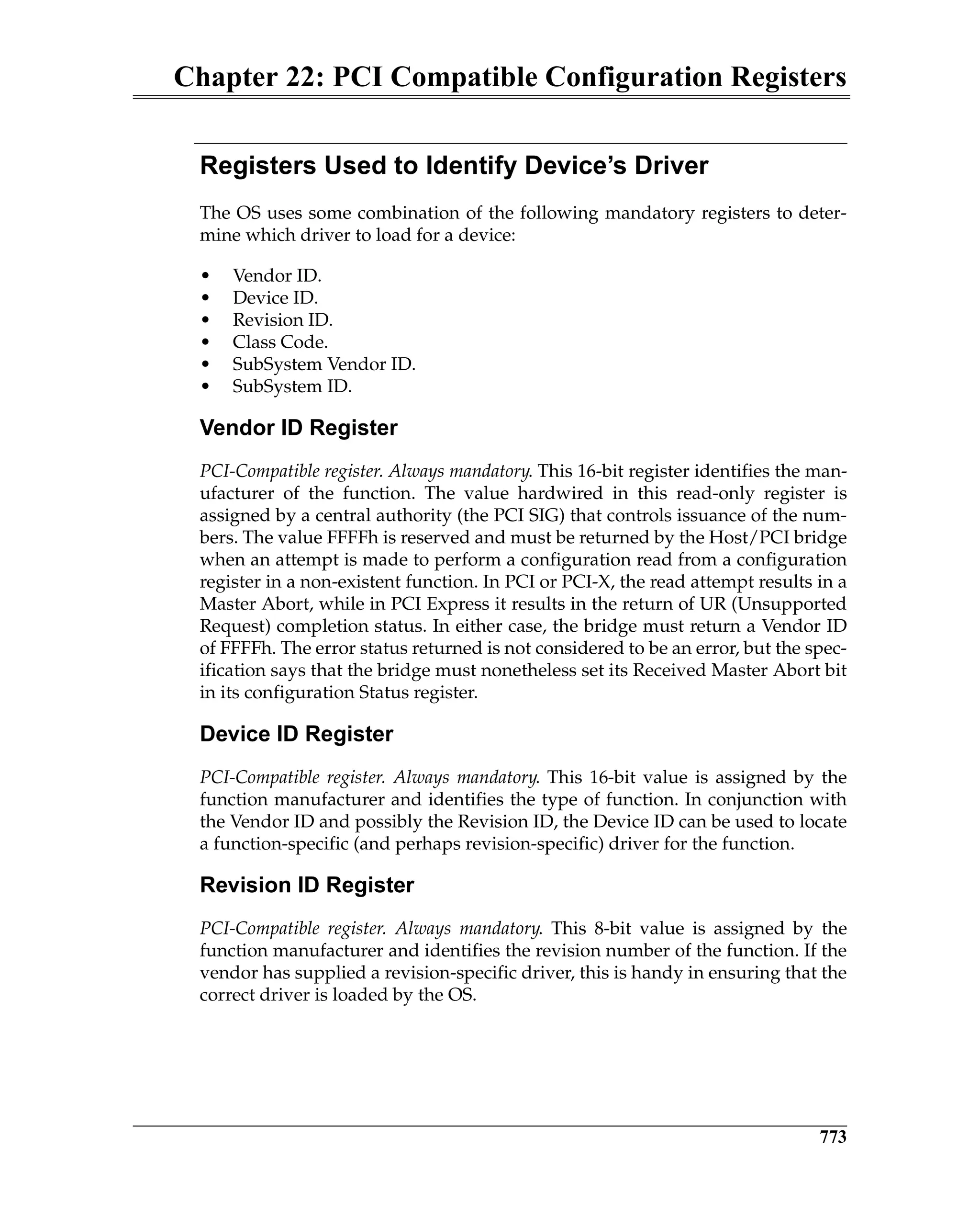
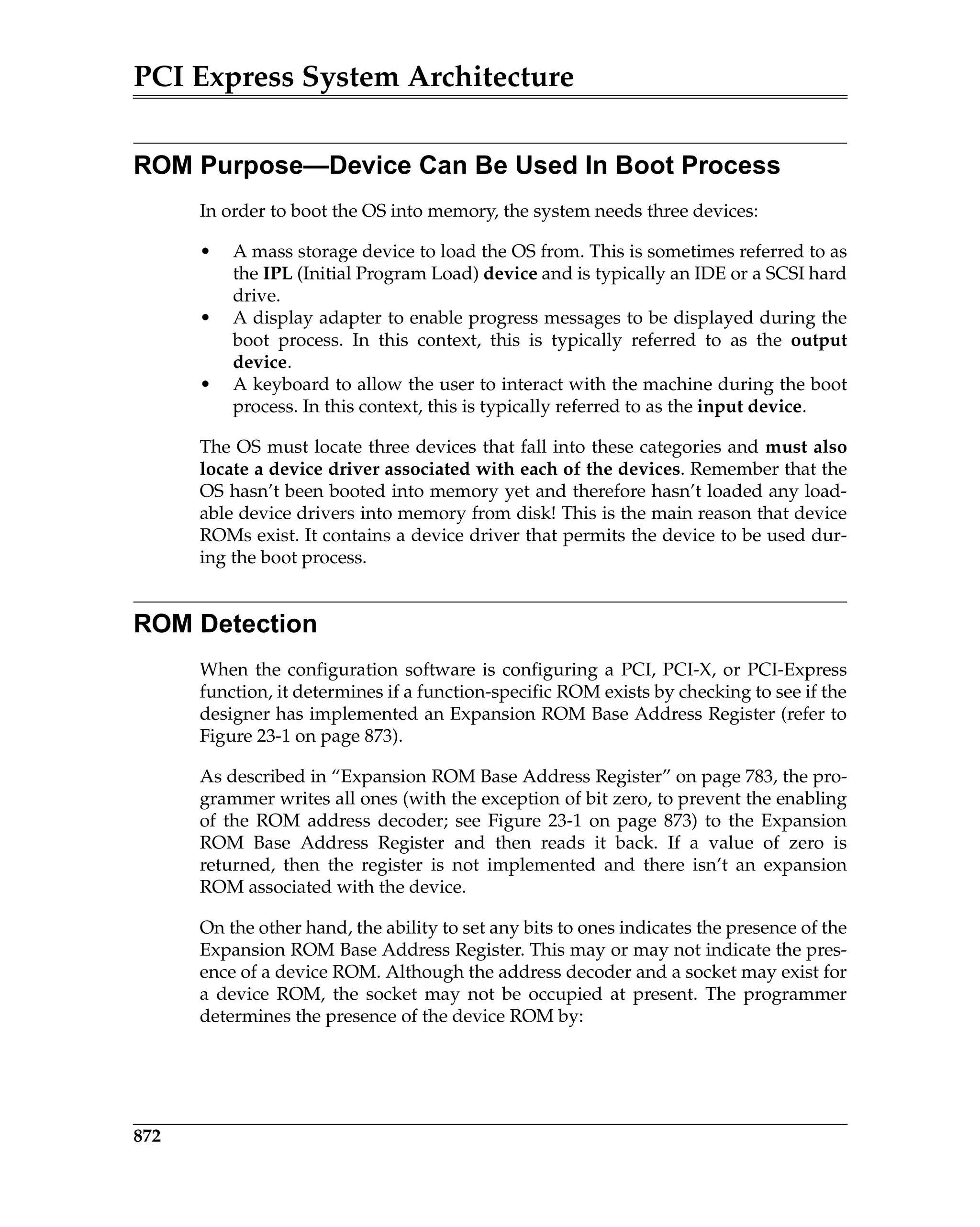
Figure 23-1 on page 873 illustrates the format of the Expansion ROM Base
Address Register. Assume that the register returns a value of FFFE0000h when
read back after writing all ones to it. Bit 17 is the least-significant bit that was
successfully changed to a one and has a binary-weighted value of 128K. This
indicates that it is a 128KB ROM decoder and bits [24:17] within the Base
Address field are writable. The programmer now writes a 32-bit start address
into the register and sets bit zero to one to enable its ROM address decoder. The
function’s ROM address decoder is then enabled and the ROM (if present) can
be accessed. The maximum ROM decoder size permitted by the PCI spec is
16MB, dictating that bits [31:25] must be read/write.
The programmer then performs a read from the first two locations of the ROM
and checks for a return value of AA55h. If this pattern is not received, the ROM
is not present. The programmer disables the ROM address decoder (by clearing
bit zero of the Expansion ROM Base Address Register to zero). If AA55h is
received, the ROM exists and a device driver code image must be copied into
main memory and its initialization code must be executed. This topic is covered
in the sections that follow.
Figure 23-1: Expansion ROM Base Address Register Bit Assignment](https://image.slidesharecdn.com/pciexpresssystemarchitecture-240110064541-2f1f00b9/75/pci-express-system-architecture-pdf-182-2048.jpg)