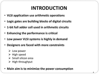
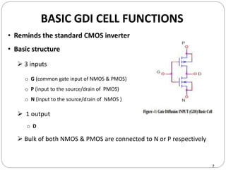
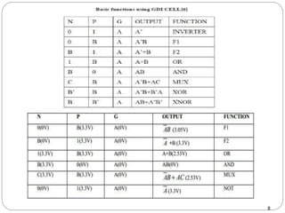
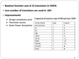
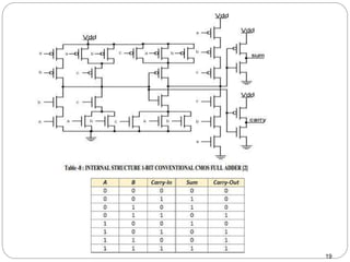
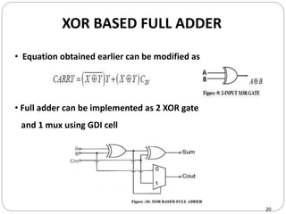
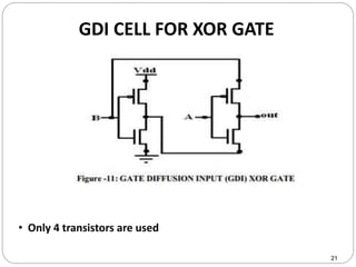
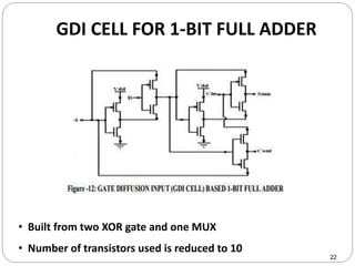
WELCOME
GRACE ABRAHAM
ROLL . NO : 01
S1 MTECH VLSI & ES
FISAT
IMPLEMENTATION OF 1-BIT FULL ADDER
USING GATE DIFFUSION INPUT (GDI)
TECHNIQUE
2
CONTENTS
• INTRODUCTION
• ADVANTAGES OF GDI OVER CMOS TECHNOLOGY
• BASIC GDI CELL FUNCTIONS
• TRANSIENT ANALYSIS OF BASIC GDI FUNCTIONS
• OPERATIONAL ANALYSIS
• COMPARISION WITH CMOS LOGIC STYLES
• CONVENTIONAL CMOS 1-BIT FULL ADDER
• XOR BASED FULL ADDER
• GDI 1-BIT FULL ADDER
• CONCLUSION
3
INTRODUCTION
• VLSI application use arithmetic operations
• Logic gates are building blocks of digital circuits
• 1-bit full adder cell used in arithmetic circuits
• Enhancing the performance is critical
• Low power VLSI systems is highly in demand
• Designers are faced with more constraints
• Main aim is to minimize the power consumption
 Low power
 High speed
 Small silicon area
 High throughput
4
• Why Low power ?
5
 Power dissipation limitations come in 2 ways
 Low power operation is desirable in integrated circuits
o Cooling considerations
 Large amount of energy dissipation by high speed circuits
 Heat removal by package is a limitation
o Increasing popularity of portable electronic devices
 Laptops, portable video players, cellular phones
 Batteries as power source
 Limited time of operation before they require recharging
6
ADVANTAGES OF GDI OVER CMOS
• Low power circuit design
• Allows reducing power consumption
• Reducing propagation delay
• Reducing area of digital circuit
• Maintaining low complexity of logic design
7
BASIC GDI CELL FUNCTIONS
• Reminds the standard CMOS inverter
• Basic structure
 3 inputs
 1 output
 Bulk of both NMOS & PMOS are connected to N or P respectively
o G (common gate input of NMOS & PMOS)
o P (input to the source/drain of PMOS)
o N (input to the source/drain of NMOS )
o D
8
• Boolean function uses 6-12 transistors in CMOS
• Less number of transistors are used in GDI
• Improvements
 Design complexity level
 Transistor counts
 Static Power dissipation
9
TRANSIENT ANALYSIS OF BASIC GATE
DIFFUSION INPUT (GDI) FUNCTIONS
10
• v(1) : Input voltage at G
• v(2) : Input voltage at P
• v(4) : Input voltage at N
• v(3) : Output voltage at D
11
12
13
OPERATIONAL ANALYSIS
• Problem with pass transistor logic : low voltage swing
• For function F1
• Low swing occurs in output when A=0 & B=0
• Expected Vtp = 0 v , due to poor high to low transition chara. of
PMOS Vtp =.50v
14
• Extra buffer circuitry may eliminate low voltage swing
• About 50% of GDI cell operates as regular CMOS inverter
• Used as a digital buffer for logic level restoration
• In some cases, when VDD= 1 without a swing from the previous
stages, a GDI functions as an inverter buffer and recovers the
voltage swing
15
COMPARISION WITH CMOS LOGIC STYLES
• Circuits were designed in
0.35µm twin well CMOS
technology
• Simulated using AIMSPICE
at 3.3V with load
capacitance =100 fF
16
• GDI have the lowest transistor count
• Both power and delay are less in case of GDI technique
17
CONVENTIONAL CMOS 1-BIT FULL ADDER
• In VLSI application, arithmetic operations play important role
• 1 bit full adder is building block of all operations
• CMOS 1 bit full adder
 Addition
 Subtraction
 Multiplication
 Inputs : A, B, Cin (1 bit)
 Outputs : Sum, Carry (1 bit)
• CMOS design style is not area efficient for complex gates
• CMOS full adder cell has 28 transistors
• Pseudo NMOS
• Dynamic logic
• CMOS logic
 Static power consumption is high
 Compromise noise margin
 Charge leakage
 Charge sharing
 PMOS pull up & NMOS pull down network
 Number of transistors used is high
o Requires frequent refreshing
18
19
XOR BASED FULL ADDER
• Equation obtained earlier can be modified as
• Full adder can be implemented as 2 XOR gate
and 1 mux using GDI cell
20
GDI CELL FOR XOR GATE
• Only 4 transistors are used
21
GDI CELL FOR 1-BIT FULL ADDER
• Built from two XOR gate and one MUX
• Number of transistors used is reduced to 10
22
TRANSIENT ANALYSIS OF GDI
BASED 1-BIT FULL ADDER
• Inputs : v(1) –A, v(4)-B, v(7)-Cin
• Outputs : v(8) – sum , v(9)- Cout
23
POWER-DELAY COMPARISION
24
CONCLUSION
• 2-Transistor implementation of complex logic functions
• In-cell swing restoration under certain operating conditions
• Low power design technique
• New Circuit is most energy efficient cell compared to CMOS circuits
• Issue of sequential logic design is currently being explored
• Works are going on in automation of a logic design methodology on
Gate Diffusion Input cells
25
REFERENCES
• WEBSITES
 www.ijecse.org
 ieeexplore.ieee.org/
 Implementation of 1-bit Full Adder using Gate Difuision Input (GDI)
cell,Arun Prakash Singh 1, Rohit Kumar 2:1,Electronics and Communication
Engineering Department, Northern India Engineering College,Lucknow, Uttar
Pradesh, India.2.Electronics and Communication Engineering Department,
Krishna Girls Engineering College
 A. Morgenshtein, A. Fish, I. A. Wagner,” Gate Diffusion Input (GDI) – A Novel
Power Efficient Method for Digital Circuits: A Design Methodology”, 14th
ASIC/SOC Conference, Washington D.C., USA, September 2001.
and more....
• PAPERS REFERED
26
27
THANK YOU
27

Implementation of 1 bit full adder using gate diffusion input (gdi) technique

  • 1.
  • 2.
    GRACE ABRAHAM ROLL .NO : 01 S1 MTECH VLSI & ES FISAT IMPLEMENTATION OF 1-BIT FULL ADDER USING GATE DIFFUSION INPUT (GDI) TECHNIQUE 2
  • 3.
    CONTENTS • INTRODUCTION • ADVANTAGESOF GDI OVER CMOS TECHNOLOGY • BASIC GDI CELL FUNCTIONS • TRANSIENT ANALYSIS OF BASIC GDI FUNCTIONS • OPERATIONAL ANALYSIS • COMPARISION WITH CMOS LOGIC STYLES • CONVENTIONAL CMOS 1-BIT FULL ADDER • XOR BASED FULL ADDER • GDI 1-BIT FULL ADDER • CONCLUSION 3
  • 4.
    INTRODUCTION • VLSI applicationuse arithmetic operations • Logic gates are building blocks of digital circuits • 1-bit full adder cell used in arithmetic circuits • Enhancing the performance is critical • Low power VLSI systems is highly in demand • Designers are faced with more constraints • Main aim is to minimize the power consumption  Low power  High speed  Small silicon area  High throughput 4
  • 5.
    • Why Lowpower ? 5  Power dissipation limitations come in 2 ways  Low power operation is desirable in integrated circuits o Cooling considerations  Large amount of energy dissipation by high speed circuits  Heat removal by package is a limitation o Increasing popularity of portable electronic devices  Laptops, portable video players, cellular phones  Batteries as power source  Limited time of operation before they require recharging
  • 6.
    6 ADVANTAGES OF GDIOVER CMOS • Low power circuit design • Allows reducing power consumption • Reducing propagation delay • Reducing area of digital circuit • Maintaining low complexity of logic design
  • 7.
    7 BASIC GDI CELLFUNCTIONS • Reminds the standard CMOS inverter • Basic structure  3 inputs  1 output  Bulk of both NMOS & PMOS are connected to N or P respectively o G (common gate input of NMOS & PMOS) o P (input to the source/drain of PMOS) o N (input to the source/drain of NMOS ) o D
  • 8.
  • 9.
    • Boolean functionuses 6-12 transistors in CMOS • Less number of transistors are used in GDI • Improvements  Design complexity level  Transistor counts  Static Power dissipation 9
  • 10.
    TRANSIENT ANALYSIS OFBASIC GATE DIFFUSION INPUT (GDI) FUNCTIONS 10 • v(1) : Input voltage at G • v(2) : Input voltage at P • v(4) : Input voltage at N • v(3) : Output voltage at D
  • 11.
  • 12.
  • 13.
    13 OPERATIONAL ANALYSIS • Problemwith pass transistor logic : low voltage swing • For function F1 • Low swing occurs in output when A=0 & B=0 • Expected Vtp = 0 v , due to poor high to low transition chara. of PMOS Vtp =.50v
  • 14.
    14 • Extra buffercircuitry may eliminate low voltage swing • About 50% of GDI cell operates as regular CMOS inverter • Used as a digital buffer for logic level restoration • In some cases, when VDD= 1 without a swing from the previous stages, a GDI functions as an inverter buffer and recovers the voltage swing
  • 15.
    15 COMPARISION WITH CMOSLOGIC STYLES • Circuits were designed in 0.35µm twin well CMOS technology • Simulated using AIMSPICE at 3.3V with load capacitance =100 fF
  • 16.
    16 • GDI havethe lowest transistor count • Both power and delay are less in case of GDI technique
  • 17.
    17 CONVENTIONAL CMOS 1-BITFULL ADDER • In VLSI application, arithmetic operations play important role • 1 bit full adder is building block of all operations • CMOS 1 bit full adder  Addition  Subtraction  Multiplication  Inputs : A, B, Cin (1 bit)  Outputs : Sum, Carry (1 bit)
  • 18.
    • CMOS designstyle is not area efficient for complex gates • CMOS full adder cell has 28 transistors • Pseudo NMOS • Dynamic logic • CMOS logic  Static power consumption is high  Compromise noise margin  Charge leakage  Charge sharing  PMOS pull up & NMOS pull down network  Number of transistors used is high o Requires frequent refreshing 18
  • 19.
  • 20.
    XOR BASED FULLADDER • Equation obtained earlier can be modified as • Full adder can be implemented as 2 XOR gate and 1 mux using GDI cell 20
  • 21.
    GDI CELL FORXOR GATE • Only 4 transistors are used 21
  • 22.
    GDI CELL FOR1-BIT FULL ADDER • Built from two XOR gate and one MUX • Number of transistors used is reduced to 10 22
  • 23.
    TRANSIENT ANALYSIS OFGDI BASED 1-BIT FULL ADDER • Inputs : v(1) –A, v(4)-B, v(7)-Cin • Outputs : v(8) – sum , v(9)- Cout 23
  • 24.
  • 25.
    CONCLUSION • 2-Transistor implementationof complex logic functions • In-cell swing restoration under certain operating conditions • Low power design technique • New Circuit is most energy efficient cell compared to CMOS circuits • Issue of sequential logic design is currently being explored • Works are going on in automation of a logic design methodology on Gate Diffusion Input cells 25
  • 26.
    REFERENCES • WEBSITES  www.ijecse.org ieeexplore.ieee.org/  Implementation of 1-bit Full Adder using Gate Difuision Input (GDI) cell,Arun Prakash Singh 1, Rohit Kumar 2:1,Electronics and Communication Engineering Department, Northern India Engineering College,Lucknow, Uttar Pradesh, India.2.Electronics and Communication Engineering Department, Krishna Girls Engineering College  A. Morgenshtein, A. Fish, I. A. Wagner,” Gate Diffusion Input (GDI) – A Novel Power Efficient Method for Digital Circuits: A Design Methodology”, 14th ASIC/SOC Conference, Washington D.C., USA, September 2001. and more.... • PAPERS REFERED 26
  • 27.