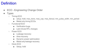
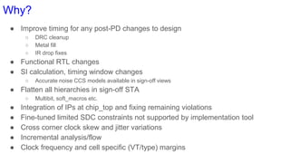
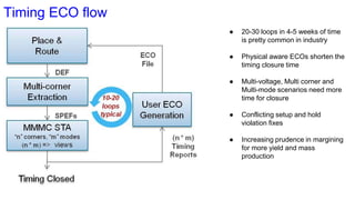
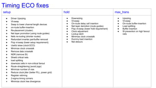
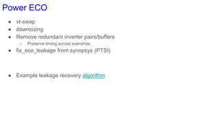
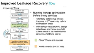
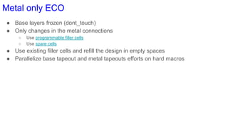
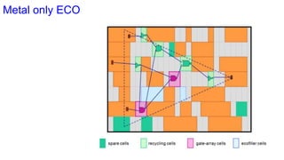
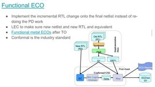
This document discusses engineering change orders (ECOs) used to fix timing, functional, power, and clock issues after physical design and sign-off. It describes the motivation for ECOs due to tool limitations and differences between implementation and sign-off. Common ECO techniques are listed for timing (driver upsizing, buffer insertion, etc.), power (vt-swapping, downsizing, etc.), and metal-only ECOs. Timing ECO tools from Synopsys, Cadence, and other vendors are also mentioned. Upcoming ECO technologies like dynamic power optimization and automatic legalization are noted.
https://www.udemy.com/vlsi-academy
Usually, while drawing any circuit on paper, we have only one 'vdd' at the top and one 'vss' at the bottom. But on a chip, it becomes necessary to have a grid structure of power, with more than one 'vdd' and 'vss'. The concept of power grid structure would be uploaded soon. It is actually the scaling trend that drives chip designers for power grid structure.
Timing and Design Closure in Physical Design Flows Olivier Coudert
A physical design flow consists of producing a production-worthy layout from a gate-level netlist subject to a set of constraints. We focus on the problems imposed by shrinking process technologies. It exposes the problems of timing closure, signal integrity, design variable dependencies, clock and power/ground routing, and design signoff. It also surveys some physical design flows, and outlines a refinement-based flow.
Clock Tree Synthesis is a technique for distributing the clock equally among all sequential parts of a VLSI design. The purpose of Clock Tree Synthesis is to reduce skew and delay. Clock Tree Synthesis is provided the placement data as well as the clock tree limitations as input. Clock Tree Synthesis (CTS) is the technique of balancing the clock delay to all clock inputs by inserting buffers/inverters along the clock routes of an ASIC design. As a result, CTS is used to balance the skew and reduce insertion latency. Before Clock Tree Synthesis, all clock pins were driven by a single clock source. Clock tree synthesis includes both clock tree construction and clock tree balance. Clock tree inverters may be used to create a clock tree that maintains the correct transition (duty cycle), and clock tree buffers (CTB) can balance the clock tree to fulfil the skew and latency requirements. To fulfil the space and power limits, fewer clock tree inverters and buffers should be employed.
Define Width and Height of Core and Die (http://www.vlsisystemdesign.com/PD-F...VLSI SYSTEM Design
https://www.udemy.com/vlsi-academy
The very first step in chip design is floorplanning, in which the width and height of the chip, basically the area of the chip, is defined. A chip consists of two parts, 'core' and 'die'.
Fusion Compiler is the next-generation RTL-to-GDSII implementation system architected to address the complexities of advanced node designs and deliver up to 20% improved PPA while reducing Time To Results (TTR) by 2X.
In this course, you
● Identify and apply timing arc information from a library, such as unateness, delays, and slew
● Identify cell delays from a library and calculate output slew degradation
● Use wire-load information to calculate net delays
● Identify the properties of a clock, including period, edges, and slew, and calculate the duty cycle
● Apply setup and hold checks to diagnose design violations
● Identify timing path types to calculate slack values
● Set environmental constraints, clocks constraints, and path exceptions
● Constrain a design using SDC
● Analyze reports to identify timing problems
VLSI Physical Design Flow(http://www.vlsisystemdesign.com)VLSI SYSTEM Design
Learning becomes Fun..
When tedious & difficult topics like Chip Design are explained in simple n creative videos....https://www.udemy.com/vlsi-academy
In electronics, crosstalk is any phenomenon by which a signal transmitted on one circuit or channel of a transmission system creates an undesired effect in another circuit or channel. Crosstalk is usually caused by undesired capacitive, inductive, or conductive coupling from one circuit or channel to another.
Crosstalk is a significant issue in structured cabling, audio electronics, integrated circuit design, wireless communication and other communications systems.
A typical design flow follows the below structure and can be broken down into multiple steps. Some of these phases happen in parallel and some in sequentially.
Requirements
A customer of a semiconductor firm is typically some other company who plans to use the chip in its systems or end products. So, the customer's requirements also play an important role in deciding how the chip should be designed.
The first step is to collect the requirements, estimate the end product's market value, and evaluate the number of resources required to do the project.
Specifications
The next step is to collect specifications that describe the functionality, interface abstractly, and over all architecture of the chip to be designed. This can be something along the lines such as:
Play
Next
Unmute
Current TimeÂ
0:00
/
DurationÂ
18:10
Â
Fullscreen
Backward Skip 10s
Play Video
Forward Skip 10s
Requires computational power to run imaging algorithms to support virtual reality.
Requires two ARM A53 processors with coherent interconnect and should run at 600 MHz.
Requires USB 3.0, Bluetooth, and PCIe 2nd gen interfaces.
It should support 1920x1080 pixel displays with an appropriate controller.
Digital Design
Because of the complex nature of modern chips, it's impossible to build something from scratch, and in many cases, many components will be reused.
For example, company A requires a FlexCAN module to interact with other modules in an automobile. They can either buy the FlexCAN design from another company to save time and effort or spend resources to build one.
It's not practical to design such a system from basic building blocks such as flip-flops and CMOS transistors.
Instead, a behavioral description is developed to analyze the design in terms of functionality, performance, and other high-level issues using a Hardware Description Language such as Verilog or VHDL.
This is usually done by a digital designer and is similar to a high-level computer programmer equipped with digital electronics skills.
Verification
Once the RTL design is ready, it needs to be verified for functional correctness.
For example, a DSP processor is expected to issue bus transactions with fetching instructions from memory and know that this will happen as expected.
The functional verification is required at this point, which is done with EDA simulators' help that can model the design and apply a different stimulus to it. This is the job of a pre-silicon verification engineer.
Logic Synthesis
Now we will convert this design into hardware schematic with real elements such as combinational gates and flip-flops. This step is called synthesis.
Logic synthesis tools enable the conversion of RTL description in HDL to a gate-level netlist. This netlist is a description of the circuit in terms of gates and connections between them.
Logic synthesis tools ensure that the netlist meets timing, area, and power specifications. Typically, they have access to different technology node
https://www.udemy.com/vlsi-academy
Usually, while drawing any circuit on paper, we have only one 'vdd' at the top and one 'vss' at the bottom. But on a chip, it becomes necessary to have a grid structure of power, with more than one 'vdd' and 'vss'. The concept of power grid structure would be uploaded soon. It is actually the scaling trend that drives chip designers for power grid structure.
Timing and Design Closure in Physical Design Flows Olivier Coudert
A physical design flow consists of producing a production-worthy layout from a gate-level netlist subject to a set of constraints. We focus on the problems imposed by shrinking process technologies. It exposes the problems of timing closure, signal integrity, design variable dependencies, clock and power/ground routing, and design signoff. It also surveys some physical design flows, and outlines a refinement-based flow.
Clock Tree Synthesis is a technique for distributing the clock equally among all sequential parts of a VLSI design. The purpose of Clock Tree Synthesis is to reduce skew and delay. Clock Tree Synthesis is provided the placement data as well as the clock tree limitations as input. Clock Tree Synthesis (CTS) is the technique of balancing the clock delay to all clock inputs by inserting buffers/inverters along the clock routes of an ASIC design. As a result, CTS is used to balance the skew and reduce insertion latency. Before Clock Tree Synthesis, all clock pins were driven by a single clock source. Clock tree synthesis includes both clock tree construction and clock tree balance. Clock tree inverters may be used to create a clock tree that maintains the correct transition (duty cycle), and clock tree buffers (CTB) can balance the clock tree to fulfil the skew and latency requirements. To fulfil the space and power limits, fewer clock tree inverters and buffers should be employed.
Define Width and Height of Core and Die (http://www.vlsisystemdesign.com/PD-F...VLSI SYSTEM Design
https://www.udemy.com/vlsi-academy
The very first step in chip design is floorplanning, in which the width and height of the chip, basically the area of the chip, is defined. A chip consists of two parts, 'core' and 'die'.
Fusion Compiler is the next-generation RTL-to-GDSII implementation system architected to address the complexities of advanced node designs and deliver up to 20% improved PPA while reducing Time To Results (TTR) by 2X.
In this course, you
● Identify and apply timing arc information from a library, such as unateness, delays, and slew
● Identify cell delays from a library and calculate output slew degradation
● Use wire-load information to calculate net delays
● Identify the properties of a clock, including period, edges, and slew, and calculate the duty cycle
● Apply setup and hold checks to diagnose design violations
● Identify timing path types to calculate slack values
● Set environmental constraints, clocks constraints, and path exceptions
● Constrain a design using SDC
● Analyze reports to identify timing problems
VLSI Physical Design Flow(http://www.vlsisystemdesign.com)VLSI SYSTEM Design
Learning becomes Fun..
When tedious & difficult topics like Chip Design are explained in simple n creative videos....https://www.udemy.com/vlsi-academy
In electronics, crosstalk is any phenomenon by which a signal transmitted on one circuit or channel of a transmission system creates an undesired effect in another circuit or channel. Crosstalk is usually caused by undesired capacitive, inductive, or conductive coupling from one circuit or channel to another.
Crosstalk is a significant issue in structured cabling, audio electronics, integrated circuit design, wireless communication and other communications systems.
A typical design flow follows the below structure and can be broken down into multiple steps. Some of these phases happen in parallel and some in sequentially.
Requirements
A customer of a semiconductor firm is typically some other company who plans to use the chip in its systems or end products. So, the customer's requirements also play an important role in deciding how the chip should be designed.
The first step is to collect the requirements, estimate the end product's market value, and evaluate the number of resources required to do the project.
Specifications
The next step is to collect specifications that describe the functionality, interface abstractly, and over all architecture of the chip to be designed. This can be something along the lines such as:
Play
Next
Unmute
Current TimeÂ
0:00
/
DurationÂ
18:10
Â
Fullscreen
Backward Skip 10s
Play Video
Forward Skip 10s
Requires computational power to run imaging algorithms to support virtual reality.
Requires two ARM A53 processors with coherent interconnect and should run at 600 MHz.
Requires USB 3.0, Bluetooth, and PCIe 2nd gen interfaces.
It should support 1920x1080 pixel displays with an appropriate controller.
Digital Design
Because of the complex nature of modern chips, it's impossible to build something from scratch, and in many cases, many components will be reused.
For example, company A requires a FlexCAN module to interact with other modules in an automobile. They can either buy the FlexCAN design from another company to save time and effort or spend resources to build one.
It's not practical to design such a system from basic building blocks such as flip-flops and CMOS transistors.
Instead, a behavioral description is developed to analyze the design in terms of functionality, performance, and other high-level issues using a Hardware Description Language such as Verilog or VHDL.
This is usually done by a digital designer and is similar to a high-level computer programmer equipped with digital electronics skills.
Verification
Once the RTL design is ready, it needs to be verified for functional correctness.
For example, a DSP processor is expected to issue bus transactions with fetching instructions from memory and know that this will happen as expected.
The functional verification is required at this point, which is done with EDA simulators' help that can model the design and apply a different stimulus to it. This is the job of a pre-silicon verification engineer.
Logic Synthesis
Now we will convert this design into hardware schematic with real elements such as combinational gates and flip-flops. This step is called synthesis.
Logic synthesis tools enable the conversion of RTL description in HDL to a gate-level netlist. This netlist is a description of the circuit in terms of gates and connections between them.
Logic synthesis tools ensure that the netlist meets timing, area, and power specifications. Typically, they have access to different technology node
Mirko Damiani - An Embedded soft real time distributed system in Golinuxlab_conf
An embedded system usually involves low level languages like C and highly customized hardware. In this talk we will see a use case of a soft real time system which was developed taking a very different approach, written in Go. We will see what are the advantages of this choice, along with its limits.
Microprocessors are used extensively in the design of any computing facility. It contains units to carry out arithmetic and logic calculations, fast storage in terms of registers and associated control logic to get instructions from memory and execute them. A number of devices can be interfaced with them to develop a complete system application. On the other hand, microcontrollers are single chip computers, integrating processor, memory and other peripheral modules into a single System-on-Chip (SoC). Apart from input-output ports, the peripherals often include timers, data converters, communication modules, and so on. The single chip solution makes the footprint of the computational element small in the overall system package, eliminating the necessity of additional chips on board. However, there exists a large range of such products. While the simpler microcontrollers are cheap, their capabilities (in terms of program size and analog and digital peripherals) are also limited. Such processors may be suitable for small applications. Microcontrollers like 8051, PIC belong to this category. On the other hand, advanced microcontrollers are often much more powerful, comparable to the very advanced microprocessors. The AVR and ARM processors are of this category.
High Speed Design Closure Techniques-Balachander KrishnamurthyMassimo Talia
Digital electronics and electronics are not only theory as many Italians are thinking. The investments in electronic design in Italy are very low, since there's the Asian market which specialized their people to the Electronics culture. So The italian electronic engineers are compared to Sciencists, but they're designers of Manifacturing. This webinar describes the main steps and techniques, in order to design a Digital Circuits, to evaluate the timing constraints and the hardware requirements. The webinar is promoted by Xilinx.
A 2015 performance study by Brendan Gregg, Nitesh Kant, and Ben Christensen. Original is in https://github.com/Netflix-Skunkworks/WSPerfLab/tree/master/test-results
Professional training institute (PTI) is an embedded training institute in Bangalore, which is well recognized for providing quality training institute in advance fields such as Embedded System, C, Linux, CAN, Basic electronics, digital electronics, presently those are the hottest and best job-providing sectors. In this presentation, We provide our syllabus of the embedded institute in Bangalore. As the world developing fast, the technologies also developing day by day, We update our syllabus after every six months, we train the students according to the present using technologies in the industries. With Professional Training Institute, You get practical training such a way that our student getting an edge over others. Our main slogan is to focus on practical and hands-on training to the student so that they are able to face any kind of interview in the embedded domain.
Power reduction techniques are important for the modern VLSI designs. Power is the today's major concern when we come to optimal trade off between area, performance and power.
Computational fluid dynamics (CFD) is frequently used in the initial design stages of industrial pump design, analyzing the overall performance as well as more specific aspects, ultimately as a tool to determine ways in which it can be improved.
In the last two years, Netflix has seen a mass migration to Spark from Pig and other MR engines. This talk will focus on the challenges of that migration and the work that has made it possible. This will include contributions that Netflix has made to Spark to enable wider adoption and on-going projects to make Spark appeal to a broader range of analysts, beyond data and ML engineers.
Speaker Ryan Blue
Semiconductor engineering is becoming more dynamic fiels since the technology scaling is taking place. Power reduction techniques are lucrative solutions to the performance, area and power trade off. Therefore Power reduction of VLSI designs are critical.
Final project report on grocery store management system..pdfKamal Acharya
In today’s fast-changing business environment, it’s extremely important to be able to respond to client needs in the most effective and timely manner. If your customers wish to see your business online and have instant access to your products or services.
Online Grocery Store is an e-commerce website, which retails various grocery products. This project allows viewing various products available enables registered users to purchase desired products instantly using Paytm, UPI payment processor (Instant Pay) and also can place order by using Cash on Delivery (Pay Later) option. This project provides an easy access to Administrators and Managers to view orders placed using Pay Later and Instant Pay options.
In order to develop an e-commerce website, a number of Technologies must be studied and understood. These include multi-tiered architecture, server and client-side scripting techniques, implementation technologies, programming language (such as PHP, HTML, CSS, JavaScript) and MySQL relational databases. This is a project with the objective to develop a basic website where a consumer is provided with a shopping cart website and also to know about the technologies used to develop such a website.
This document will discuss each of the underlying technologies to create and implement an e- commerce website.
Immunizing Image Classifiers Against Localized Adversary Attacksgerogepatton
This paper addresses the vulnerability of deep learning models, particularly convolutional neural networks
(CNN)s, to adversarial attacks and presents a proactive training technique designed to counter them. We
introduce a novel volumization algorithm, which transforms 2D images into 3D volumetric representations.
When combined with 3D convolution and deep curriculum learning optimization (CLO), itsignificantly improves
the immunity of models against localized universal attacks by up to 40%. We evaluate our proposed approach
using contemporary CNN architectures and the modified Canadian Institute for Advanced Research (CIFAR-10
and CIFAR-100) and ImageNet Large Scale Visual Recognition Challenge (ILSVRC12) datasets, showcasing
accuracy improvements over previous techniques. The results indicate that the combination of the volumetric
input and curriculum learning holds significant promise for mitigating adversarial attacks without necessitating
adversary training.
Water scarcity is the lack of fresh water resources to meet the standard water demand. There are two type of water scarcity. One is physical. The other is economic water scarcity.
2. Agenda
● Motivation
● Flow
● Specific types of ECOs and examples
● Timing ECO tools
● Conclusions
* Various hyperlinks provided for an in-depth study
3. Definition
● ECO - Engineering Change Order
● Types
○ Timing ECO
■ setup, hold, max_trans, max_cap, max_fanout, min_pulse_width, min_period
■ Metal only timing ECOs
○ Functional ECO
■ Verification bugs
■ Last minute RTL changes
○ Power ECO
■ Leakage recovery
■ Area recovery
■ Dynamic power optimization
■ Metal only leakage recovery
○ Clock ECO
■ Setup, hold
4. Why?
● Implementation tool doesn’t fix all the violations
● Mis-correlation between implementation and sign-off
○ GBA/PBA
○ Sign-off margins are different from PD margins
○ PnR spef (less accurate) v.s. STARRC spef (sign-off)
○ Delay calculation
○ Modeling differences (NDM, .lib, CCS)
○ OCV modeling differences
● More sign-off corners than what is enabled in PnR
● Verification catches bugs
○ Do not want to restart PD, but directly change netlist
● Recover power based on sign-off views
● DFT mode hold violations
● Incremental changes to the design towards closure
○ Revert back the changes if progressing in a wrong direction
5. Why?
● Improve timing for any post-PD changes to design
○ DRC cleanup
○ Metal fill
○ IR drop fixes
● Functional RTL changes
● SI calculation, timing window changes
○ Accurate noise CCS models available in sign-off views
● Flatten all hierarchies in sign-off STA
○ Multibit, soft_macros etc.
● Integration of IPs at chip_top and fixing remaining violations
● Fine-tuned limited SDC constraints not supported by implementation tool
● Cross corner clock skew and jitter variations
● Incremental analysis/flow
● Clock frequency and cell specific (VT/type) margins
6. Need for physical aware ECOs
● Lot of iterations for design closure
○ Back and forth between PD and sign-off
○ Less correlation leads to more iterations
● Lower technology nodes have restrictive rules
○ min_vt_spacing
○ min_vt_area
○ cell specific derates
○ Need for R,C estimation during ECO generation
○ Double patterning DRC violations
● Miscorrelation between estimated and actual routes
● Lower technology nodes demand physical awareness
● Shorter Turnaround time
● Complex IPs and integration needs more automation
7. Timing ECO flow
● 20-30 loops in 4-5 weeks of time
is pretty common in industry
● Physical aware ECOs shorten the
timing closure time
● Multi-voltage, Multi corner and
Multi-mode scenarios need more
time for closure
● Conflicting setup and hold
violation fixes
● Increasing prudence in margining
for more yield and mass
production
11. Metal only ECO
● Base layers frozen (dont_touch)
● Only changes in the metal connections
○ Use programmable filler cells
○ Use spare cells
● Use existing filler cells and refill the design in empty spaces
● Parallelize base tapeout and metal tapeouts efforts on hard macros
14. Functional ECO
● Implement the incremental RTL change onto the final netlist instead of re-
doing the PD work
● LEC to make sure new netlist and new RTL and equivalent
● Functional metal ECOs after TO
● Conformal is the industry standard
15. Upcoming Technologies
● Clock ECO
○ setup/hold fixes
● Dynamic power optimization
○ SAIF/VCD/Toggle rate
● Route control in timing ECOs
● Automatic mapping and legalization for functional ECO gates
● Robust Minimal Physical Impact flows
● Local placement re-clustering algorithms