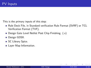
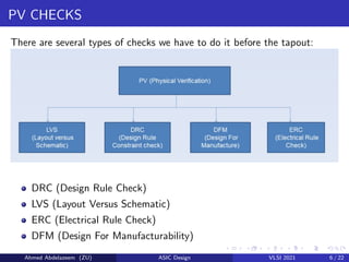
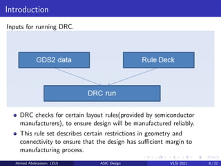
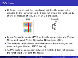
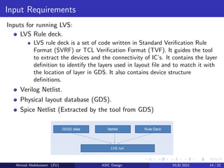
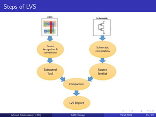
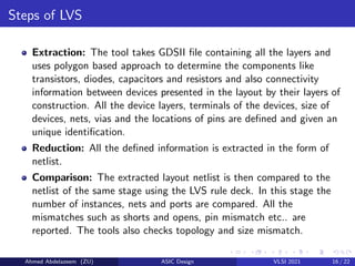
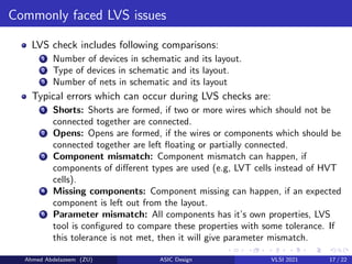
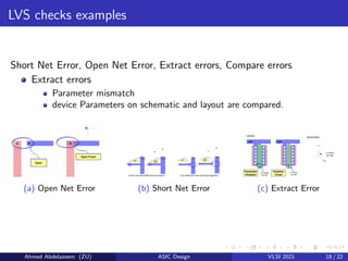
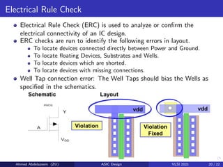
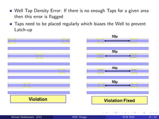
Physical Design Verification
Introduction
A. Abdelazeem1
1Faculty of Engineering
Zagazig University
RTL2GDS Flow, November 2022
Ahmed Abdelazeem (ZU) ASIC Design VLSI 2021 1 / 22
Table of Contents
1 Introduction
2 Design Rules Check(DRC)
3 Layout Versus Schematic (LVS)
4 Electrical Rule Check (ERC)
Ahmed Abdelazeem (ZU) ASIC Design VLSI 2021 2 / 22
Table of Contents
1 Introduction
2 Design Rules Check(DRC)
3 Layout Versus Schematic (LVS)
4 Electrical Rule Check (ERC)
Ahmed Abdelazeem (ZU) ASIC Design VLSI 2021 3 / 22
Introduction
It is process where an integrated circuit layout design is verified to ensure
correct electrical, logical functionality and manufacturability
Physical Verification checks are done on design (GDSII) to assure
that design is clean.
We use standalone setup to run each PVR check on the GDSII and
Spice
The routed design is checked for collecting rules criteria as for the
foundry.
The Tools used in this steps are:
Hercules and IC-Validator(ICV) from Synopsys.
Calibre from Siemens.
Assura from Cadence.
Ahmed Abdelazeem (ZU) ASIC Design VLSI 2021 4 / 22
PV Inputs
This is the primary inputs of this step:
Rule Deck File, in Standard verification Rule Format (SVRF) or TCL
Verification Format (TVF).
Design Gate Level Netlist Post Chip Finishing. (.v)
Design GDSII.
SC Library Spice.
Layer Map Information.
Ahmed Abdelazeem (ZU) ASIC Design VLSI 2021 5 / 22
PV CHECKS
There are several types of checks we have to do it before the tapout:
DRC (Design Rule Check)
LVS (Layout Versus Schematic)
ERC (Electrical Rule Check)
DFM (Design For Manufacturability)
Ahmed Abdelazeem (ZU) ASIC Design VLSI 2021 6 / 22
Table of Contents
1 Introduction
2 Design Rules Check(DRC)
3 Layout Versus Schematic (LVS)
4 Electrical Rule Check (ERC)
Ahmed Abdelazeem (ZU) ASIC Design VLSI 2021 7 / 22
Introduction
Inputs for running DRC.
DRC checks for certain layout rules(provided by semiconductor
manufacturers), to ensure design will be manufactured reliably.
This rule set describes certain restrictions in geometry and
connectivity to ensure that the design has sufficient margin to
manufacturing process.
Ahmed Abdelazeem (ZU) ASIC Design VLSI 2021 8 / 22
Design Rule examples
Minimum Spacing: The minimum spacing between objects on a
single layer.
Minimum Width: The min width rule specifies the minimum width
of individual shapes on a single layer.
Minimum Enclosure/ Overlap: Implies that the second layer is fully
enclosed by the first one.
Minimum Enclosure/ Overlap: Implies that the second layer is fully
enclosed by the first one.
Minimum Cut: the minimum number of cuts a via must have when
it is on a wide wire
Notch: The rule specifies the minimum spacing rule for objects on
the same net, including defining the minimum notch on a single-layer,
merged object
Ahmed Abdelazeem (ZU) ASIC Design VLSI 2021 9 / 22
Design Rule examples
Some of the Violations:
Ahmed Abdelazeem (ZU) ASIC Design VLSI 2021 10 / 22
DRC Categories
DRC have 2 categories – Base Layer DRC’s and Metal DRC’s
Base Layer DRC’s: Base layer means all layers upto contact/metal1.
In Base layer, DRC flow rules will be checked:
1 Base DRC’s are spacing rules for geometries inside transistor (Well
spacing, Poly spacing, Poly width).
2 Tap cell requirement.
3 Well continuity (after routing fill empty space using spare cells)
Fixes: Most of the times, base DRC’s will be clean if we ensure two
conditions.
1 Make sure design is placed legally.
2 No cell overlaps & no gaps
Metal DRC’s: Metal DRC means from contact to all the routing
layers. Basic metal DRC’s are:
1 Width (min & max)
2 Spacing (min)
3 Via enclosure (size of min cut, min via to via spacing in multi cut Vias)
Ahmed Abdelazeem (ZU) ASIC Design VLSI 2021 11 / 22
Table of Contents
1 Introduction
2 Design Rules Check(DRC)
3 Layout Versus Schematic (LVS)
4 Electrical Rule Check (ERC)
Ahmed Abdelazeem (ZU) ASIC Design VLSI 2021 12 / 22
LVS Flow
DRC only verifies that the given layout satisfies the design rules
provided by the fabrication unit. It does not ensure the functionality
of layout. Because of this, idea of LVS is orginated.
Layout Versus Schematic (LVS) verifies the connectivity of a Verilog
Netlist and Layout Netlist (Extracted Netlist from GDS).
Tool extracts circuit devices and interconnects from the layout and
saved as Layout Netlist (SPICE format).
As LVS performs comparison between 2 Netlist, it does not compare
the functionalities of both the Netlist.
Ahmed Abdelazeem (ZU) ASIC Design VLSI 2021 13 / 22
Input Requirements
Inputs for running LVS:
LVS Rule deck.
LVS rule deck is a set of code written in Standard Verification Rule
Format (SVRF) or TCL Verification Format (TVF). It guides the tool
to extract the devices and the connectivity of IC’s. It contains the layer
definition to identify the layers used in layout file and to match it with
the location of layer in GDS. It also contains device structure
definitions.
Verilog Netlist.
Physical layout database (GDS).
Spice Netlist (Extracted by the tool from GDS)
Ahmed Abdelazeem (ZU) ASIC Design VLSI 2021 14 / 22
Steps of LVS
Ahmed Abdelazeem (ZU) ASIC Design VLSI 2021 15 / 22
Steps of LVS
Extraction: The tool takes GDSII file containing all the layers and
uses polygon based approach to determine the components like
transistors, diodes, capacitors and resistors and also connectivity
information between devices presented in the layout by their layers of
construction. All the device layers, terminals of the devices, size of
devices, nets, vias and the locations of pins are defined and given an
unique identification.
Reduction: All the defined information is extracted in the form of
netlist.
Comparison: The extracted layout netlist is then compared to the
netlist of the same stage using the LVS rule deck. In this stage the
number of instances, nets and ports are compared. All the
mismatches such as shorts and opens, pin mismatch etc.. are
reported. The tools also checks topology and size mismatch.
Ahmed Abdelazeem (ZU) ASIC Design VLSI 2021 16 / 22
Commonly faced LVS issues
LVS check includes following comparisons:
1 Number of devices in schematic and its layout.
2 Type of devices in schematic and its layout.
3 Number of nets in schematic and its layout
Typical errors which can occur during LVS checks are:
1 Shorts: Shorts are formed, if two or more wires which should not be
connected together are connected.
2 Opens: Opens are formed, if the wires or components which should be
connected together are left floating or partially connected.
3 Component mismatch: Component mismatch can happen, if
components of different types are used (e.g, LVT cells instead of HVT
cells).
4 Missing components: Component missing can happen, if an expected
component is left out from the layout.
5 Parameter mismatch: All components has it’s own properties, LVS
tool is configured to compare these properties with some tolerance. If
this tolerance is not met, then it will give parameter mismatch.
Ahmed Abdelazeem (ZU) ASIC Design VLSI 2021 17 / 22
LVS checks examples
Short Net Error, Open Net Error, Extract errors, Compare errors
Extract errors
Parameter mismatch
device Parameters on schematic and layout are compared.
(a) Open Net Error (b) Short Net Error (c) Extract Error
Ahmed Abdelazeem (ZU) ASIC Design VLSI 2021 18 / 22
Compare Errors
Malformed Devices
Pin Errors
Device Mismatch
Net Mismatch
(a) Malformed Devices (b) Pin Errors (c) Net Mismatch
Ahmed Abdelazeem (ZU) ASIC Design VLSI 2021 19 / 22
Table of Contents
1 Introduction
2 Design Rules Check(DRC)
3 Layout Versus Schematic (LVS)
4 Electrical Rule Check (ERC)
Ahmed Abdelazeem (ZU) ASIC Design VLSI 2021 19 / 22
Electrical Rule Check
Electrical Rule Check (ERC) is used to analyze or confirm the
electrical connectivity of an IC design.
ERC checks are run to identify the following errors in layout.
To locate devices connected directly between Power and Ground.
To locate floating Devices, Substrates and Wells.
To locate devices which are shorted.
To locate devices with missing connections.
Well Tap connection error: The Well Taps should bias the Wells as
specified in the schematics.
Ahmed Abdelazeem (ZU) ASIC Design VLSI 2021 20 / 22
Well Tap Density Error: If there is no enough Taps for a given area
then this error is flagged
Taps need to be placed regularly which biases the Well to prevent
Latch-up
Ahmed Abdelazeem (ZU) ASIC Design VLSI 2021 21 / 22
Main References
J. Plummer “Silicon VLSI Technology”, 2000 – especially Chapter 2
Signoff Semiconductors, SignOff checks
J. Rabaey, “Digital Integrated Circuits” 2003, Chapters 2.2-2.3
Ahmed Abdelazeem (ZU) ASIC Design VLSI 2021 22 / 22

Physical Verification.pdf

  • 1.
    Physical Design Verification Introduction A.Abdelazeem1 1Faculty of Engineering Zagazig University RTL2GDS Flow, November 2022 Ahmed Abdelazeem (ZU) ASIC Design VLSI 2021 1 / 22
  • 2.
    Table of Contents 1Introduction 2 Design Rules Check(DRC) 3 Layout Versus Schematic (LVS) 4 Electrical Rule Check (ERC) Ahmed Abdelazeem (ZU) ASIC Design VLSI 2021 2 / 22
  • 3.
    Table of Contents 1Introduction 2 Design Rules Check(DRC) 3 Layout Versus Schematic (LVS) 4 Electrical Rule Check (ERC) Ahmed Abdelazeem (ZU) ASIC Design VLSI 2021 3 / 22
  • 4.
    Introduction It is processwhere an integrated circuit layout design is verified to ensure correct electrical, logical functionality and manufacturability Physical Verification checks are done on design (GDSII) to assure that design is clean. We use standalone setup to run each PVR check on the GDSII and Spice The routed design is checked for collecting rules criteria as for the foundry. The Tools used in this steps are: Hercules and IC-Validator(ICV) from Synopsys. Calibre from Siemens. Assura from Cadence. Ahmed Abdelazeem (ZU) ASIC Design VLSI 2021 4 / 22
  • 5.
    PV Inputs This isthe primary inputs of this step: Rule Deck File, in Standard verification Rule Format (SVRF) or TCL Verification Format (TVF). Design Gate Level Netlist Post Chip Finishing. (.v) Design GDSII. SC Library Spice. Layer Map Information. Ahmed Abdelazeem (ZU) ASIC Design VLSI 2021 5 / 22
  • 6.
    PV CHECKS There areseveral types of checks we have to do it before the tapout: DRC (Design Rule Check) LVS (Layout Versus Schematic) ERC (Electrical Rule Check) DFM (Design For Manufacturability) Ahmed Abdelazeem (ZU) ASIC Design VLSI 2021 6 / 22
  • 7.
    Table of Contents 1Introduction 2 Design Rules Check(DRC) 3 Layout Versus Schematic (LVS) 4 Electrical Rule Check (ERC) Ahmed Abdelazeem (ZU) ASIC Design VLSI 2021 7 / 22
  • 8.
    Introduction Inputs for runningDRC. DRC checks for certain layout rules(provided by semiconductor manufacturers), to ensure design will be manufactured reliably. This rule set describes certain restrictions in geometry and connectivity to ensure that the design has sufficient margin to manufacturing process. Ahmed Abdelazeem (ZU) ASIC Design VLSI 2021 8 / 22
  • 9.
    Design Rule examples MinimumSpacing: The minimum spacing between objects on a single layer. Minimum Width: The min width rule specifies the minimum width of individual shapes on a single layer. Minimum Enclosure/ Overlap: Implies that the second layer is fully enclosed by the first one. Minimum Enclosure/ Overlap: Implies that the second layer is fully enclosed by the first one. Minimum Cut: the minimum number of cuts a via must have when it is on a wide wire Notch: The rule specifies the minimum spacing rule for objects on the same net, including defining the minimum notch on a single-layer, merged object Ahmed Abdelazeem (ZU) ASIC Design VLSI 2021 9 / 22
  • 10.
    Design Rule examples Someof the Violations: Ahmed Abdelazeem (ZU) ASIC Design VLSI 2021 10 / 22
  • 11.
    DRC Categories DRC have2 categories – Base Layer DRC’s and Metal DRC’s Base Layer DRC’s: Base layer means all layers upto contact/metal1. In Base layer, DRC flow rules will be checked: 1 Base DRC’s are spacing rules for geometries inside transistor (Well spacing, Poly spacing, Poly width). 2 Tap cell requirement. 3 Well continuity (after routing fill empty space using spare cells) Fixes: Most of the times, base DRC’s will be clean if we ensure two conditions. 1 Make sure design is placed legally. 2 No cell overlaps & no gaps Metal DRC’s: Metal DRC means from contact to all the routing layers. Basic metal DRC’s are: 1 Width (min & max) 2 Spacing (min) 3 Via enclosure (size of min cut, min via to via spacing in multi cut Vias) Ahmed Abdelazeem (ZU) ASIC Design VLSI 2021 11 / 22
  • 12.
    Table of Contents 1Introduction 2 Design Rules Check(DRC) 3 Layout Versus Schematic (LVS) 4 Electrical Rule Check (ERC) Ahmed Abdelazeem (ZU) ASIC Design VLSI 2021 12 / 22
  • 13.
    LVS Flow DRC onlyverifies that the given layout satisfies the design rules provided by the fabrication unit. It does not ensure the functionality of layout. Because of this, idea of LVS is orginated. Layout Versus Schematic (LVS) verifies the connectivity of a Verilog Netlist and Layout Netlist (Extracted Netlist from GDS). Tool extracts circuit devices and interconnects from the layout and saved as Layout Netlist (SPICE format). As LVS performs comparison between 2 Netlist, it does not compare the functionalities of both the Netlist. Ahmed Abdelazeem (ZU) ASIC Design VLSI 2021 13 / 22
  • 14.
    Input Requirements Inputs forrunning LVS: LVS Rule deck. LVS rule deck is a set of code written in Standard Verification Rule Format (SVRF) or TCL Verification Format (TVF). It guides the tool to extract the devices and the connectivity of IC’s. It contains the layer definition to identify the layers used in layout file and to match it with the location of layer in GDS. It also contains device structure definitions. Verilog Netlist. Physical layout database (GDS). Spice Netlist (Extracted by the tool from GDS) Ahmed Abdelazeem (ZU) ASIC Design VLSI 2021 14 / 22
  • 15.
    Steps of LVS AhmedAbdelazeem (ZU) ASIC Design VLSI 2021 15 / 22
  • 16.
    Steps of LVS Extraction:The tool takes GDSII file containing all the layers and uses polygon based approach to determine the components like transistors, diodes, capacitors and resistors and also connectivity information between devices presented in the layout by their layers of construction. All the device layers, terminals of the devices, size of devices, nets, vias and the locations of pins are defined and given an unique identification. Reduction: All the defined information is extracted in the form of netlist. Comparison: The extracted layout netlist is then compared to the netlist of the same stage using the LVS rule deck. In this stage the number of instances, nets and ports are compared. All the mismatches such as shorts and opens, pin mismatch etc.. are reported. The tools also checks topology and size mismatch. Ahmed Abdelazeem (ZU) ASIC Design VLSI 2021 16 / 22
  • 17.
    Commonly faced LVSissues LVS check includes following comparisons: 1 Number of devices in schematic and its layout. 2 Type of devices in schematic and its layout. 3 Number of nets in schematic and its layout Typical errors which can occur during LVS checks are: 1 Shorts: Shorts are formed, if two or more wires which should not be connected together are connected. 2 Opens: Opens are formed, if the wires or components which should be connected together are left floating or partially connected. 3 Component mismatch: Component mismatch can happen, if components of different types are used (e.g, LVT cells instead of HVT cells). 4 Missing components: Component missing can happen, if an expected component is left out from the layout. 5 Parameter mismatch: All components has it’s own properties, LVS tool is configured to compare these properties with some tolerance. If this tolerance is not met, then it will give parameter mismatch. Ahmed Abdelazeem (ZU) ASIC Design VLSI 2021 17 / 22
  • 18.
    LVS checks examples ShortNet Error, Open Net Error, Extract errors, Compare errors Extract errors Parameter mismatch device Parameters on schematic and layout are compared. (a) Open Net Error (b) Short Net Error (c) Extract Error Ahmed Abdelazeem (ZU) ASIC Design VLSI 2021 18 / 22
  • 19.
    Compare Errors Malformed Devices PinErrors Device Mismatch Net Mismatch (a) Malformed Devices (b) Pin Errors (c) Net Mismatch Ahmed Abdelazeem (ZU) ASIC Design VLSI 2021 19 / 22
  • 20.
    Table of Contents 1Introduction 2 Design Rules Check(DRC) 3 Layout Versus Schematic (LVS) 4 Electrical Rule Check (ERC) Ahmed Abdelazeem (ZU) ASIC Design VLSI 2021 19 / 22
  • 21.
    Electrical Rule Check ElectricalRule Check (ERC) is used to analyze or confirm the electrical connectivity of an IC design. ERC checks are run to identify the following errors in layout. To locate devices connected directly between Power and Ground. To locate floating Devices, Substrates and Wells. To locate devices which are shorted. To locate devices with missing connections. Well Tap connection error: The Well Taps should bias the Wells as specified in the schematics. Ahmed Abdelazeem (ZU) ASIC Design VLSI 2021 20 / 22
  • 22.
    Well Tap DensityError: If there is no enough Taps for a given area then this error is flagged Taps need to be placed regularly which biases the Well to prevent Latch-up Ahmed Abdelazeem (ZU) ASIC Design VLSI 2021 21 / 22
  • 23.
    Main References J. Plummer“Silicon VLSI Technology”, 2000 – especially Chapter 2 Signoff Semiconductors, SignOff checks J. Rabaey, “Digital Integrated Circuits” 2003, Chapters 2.2-2.3 Ahmed Abdelazeem (ZU) ASIC Design VLSI 2021 22 / 22