As low power circuits are most popular the decrease in supply voltage leads to increase in leakage power with respect to the technology scaling. So for removing this kind of leakages and to provide a better power efficiency many power gating techniques are used. But the leakage due to ground connection to the active part of the circuit is very high rather than all other leakages. As it is mainly due to the back EMF of the ground connection it was called it as ground bounce noise. To reduce this noise different methodologies are designed. In this paper the design of such an efficient technique related to ground bounce noise reduction using power gating circuits and comparing the results using DSCH and Microwind low power tools. In this paper the analysis of adders such as full adders using different types of power gated circuits using low power VLSI design techniques and to present the comparison results between different power gating methods.
International Journal of Engineering Research and Applications (IJERA) is an open access online peer reviewed international journal that publishes research and review articles in the fields of Computer Science, Neural Networks, Electrical Engineering, Software Engineering, Information Technology, Mechanical Engineering, Chemical Engineering, Plastic Engineering, Food Technology, Textile Engineering, Nano Technology & science, Power Electronics, Electronics & Communication Engineering, Computational mathematics, Image processing, Civil Engineering, Structural Engineering, Environmental Engineering, VLSI Testing & Low Power VLSI Design etc.
The low power has been the main concern for the VLSI industry with the technology scaling in CMOS process from 130 nm to 22nm. The presentation here gives a brief idea about the several low power VLSI techniques being used in VLSI circuits to reduce the power and delay. for any query feel free to visit us at: http://www.siliconmentor.com/
Static power optimization using dual sub threshold supply voltages in digital...VLSICS Design
Power dissipation in high performance systems requi
res more expensive packaging. In this situation, lo
w
power VLSI design has assumed great importance as a
n active and rapidly developing field. As the densi
ty
and operating speed of CMOS VLSI chip increases, st
atic power dissipation becomes more significant. Th
is
is due to the leakage current when the transistor i
s off this is threshold voltage dependent. This can
be
observed in the combinational and sequential circui
ts. Static power reduction techniques are achieved
by
means of operating the transistor either in Cut-off
or in Saturation region completely and avoiding th
e
clock in unnecessary circuits. In this work, “Dual
sub-threshold voltage supply” technique is used to
operate the transistor under off state or either in
on state by applying some voltage at the gate of t
he MOS
transistor. This static power reduction technique i
s to digital circuits, so that the power dissipatio
n is
reduced and the performance of the circuit is incre
ased. The designed circuits can be simulated by usi
ng
Mentor Graphics Backend Tool
International Journal of Engineering Research and Applications (IJERA) is an open access online peer reviewed international journal that publishes research and review articles in the fields of Computer Science, Neural Networks, Electrical Engineering, Software Engineering, Information Technology, Mechanical Engineering, Chemical Engineering, Plastic Engineering, Food Technology, Textile Engineering, Nano Technology & science, Power Electronics, Electronics & Communication Engineering, Computational mathematics, Image processing, Civil Engineering, Structural Engineering, Environmental Engineering, VLSI Testing & Low Power VLSI Design etc.
Power gating is the main power reduction techniques for the static power. As long as technology scaling is taking place, static power becomes paramount important factor to the VLSI designs.Therefore Power gating is the recent power reduction technique that is actively in research areas.
International Journal of Engineering Research and Applications (IJERA) is an open access online peer reviewed international journal that publishes research and review articles in the fields of Computer Science, Neural Networks, Electrical Engineering, Software Engineering, Information Technology, Mechanical Engineering, Chemical Engineering, Plastic Engineering, Food Technology, Textile Engineering, Nano Technology & science, Power Electronics, Electronics & Communication Engineering, Computational mathematics, Image processing, Civil Engineering, Structural Engineering, Environmental Engineering, VLSI Testing & Low Power VLSI Design etc.
The low power has been the main concern for the VLSI industry with the technology scaling in CMOS process from 130 nm to 22nm. The presentation here gives a brief idea about the several low power VLSI techniques being used in VLSI circuits to reduce the power and delay. for any query feel free to visit us at: http://www.siliconmentor.com/
Static power optimization using dual sub threshold supply voltages in digital...VLSICS Design
Power dissipation in high performance systems requi
res more expensive packaging. In this situation, lo
w
power VLSI design has assumed great importance as a
n active and rapidly developing field. As the densi
ty
and operating speed of CMOS VLSI chip increases, st
atic power dissipation becomes more significant. Th
is
is due to the leakage current when the transistor i
s off this is threshold voltage dependent. This can
be
observed in the combinational and sequential circui
ts. Static power reduction techniques are achieved
by
means of operating the transistor either in Cut-off
or in Saturation region completely and avoiding th
e
clock in unnecessary circuits. In this work, “Dual
sub-threshold voltage supply” technique is used to
operate the transistor under off state or either in
on state by applying some voltage at the gate of t
he MOS
transistor. This static power reduction technique i
s to digital circuits, so that the power dissipatio
n is
reduced and the performance of the circuit is incre
ased. The designed circuits can be simulated by usi
ng
Mentor Graphics Backend Tool
International Journal of Engineering Research and Applications (IJERA) is an open access online peer reviewed international journal that publishes research and review articles in the fields of Computer Science, Neural Networks, Electrical Engineering, Software Engineering, Information Technology, Mechanical Engineering, Chemical Engineering, Plastic Engineering, Food Technology, Textile Engineering, Nano Technology & science, Power Electronics, Electronics & Communication Engineering, Computational mathematics, Image processing, Civil Engineering, Structural Engineering, Environmental Engineering, VLSI Testing & Low Power VLSI Design etc.
Power gating is the main power reduction techniques for the static power. As long as technology scaling is taking place, static power becomes paramount important factor to the VLSI designs.Therefore Power gating is the recent power reduction technique that is actively in research areas.
Sources of Power Dissipation
Dynamic Power Dissipation
Static Power Dissipation
Power Reduction Techniques
Algorithmic Power Minimization
Architectural Power Minimization
Logic and Circuit Level Power Minimization
Control Logic Power Minimization
System Level Power Management.
International Journal of Computational Engineering Research (IJCER)ijceronline
International Journal of Computational Engineering Research(IJCER) is an intentional online Journal in English monthly publishing journal. This Journal publish original research work that contributes significantly to further the scientific knowledge in engineering and Technology.
Analysis of Power Dissipation & Low Power VLSI Chip DesignEditor IJMTER
Low power requirement has become a principal motto in today’s world of electronics
industries. Power dissipation has becoming an important consideration as performance and area for
VLSI Chip design. With reducing the chip size, reduced power consumption and power management
on chip are the key challenges due to increased complexity. Low power chip requirement in the
VLSI industry is main considerable field due to the reduction of chip dimension day by day and
environmental factors. For many designs, optimization of power is important as timing due to the
need to reduce package cost and extended battery life. This paper present various techniques to
reduce the power requirement in various stages of CMOS designing i.e. Dynamic Power
Suppression, Adiabatic Circuits, Logic Design for Low Power, Reducing Glitches, Logic Level
Power Optimization, Standby Mode Leakage Suppression, Variable Body Biasing, Sleep Transistors,
Dynamic Threshold MOS, Short Circuit Power Suppression.
Sub-Threshold Leakage Current Reduction Techniques In VLSI Circuits -A SurveyIJERA Editor
There is an increasing demand for portable devices powered up by battery, this led the manufacturers of
semiconductor technology to scale down the feature size which results in reduction in threshold voltage and
enables the complex functionality on a single chip. By scaling down the feature size the dynamic power
dissipation has no effect but the static power dissipation has become equal or more than that of Dynamic power
dissipation. So in recent CMOS technologies static power dissipation i.e. power dissipation due to leakage
current has become a challenging area for VLSI chip designers. In order to prolong the battery life and maintain
reliability of circuit, leakage current reduction is the primary goal. A basic overview of techniques used for
reduction of sub-threshold leakages is discussed in this paper. Based on the surveyed techniques, one would be
able to choose required and apt leakage reduction technique.
Power Dissipation of VLSI Circuits and Modern Techniques of Designing Low Pow...IJSRD
This paper focus on the various sources of power dissipation in modern VLSI circuits. This paper also discuss the importance of designing low power VLSI circuits along with various techniques of power reduction and its advantages and disadvantages. It is basically a comparative study between various power reduction techniques in modern VLSI circuits.
Adiabatic describe the thermodynamic processes in which there is no energy exchange with the environment, and therefore very less dissipated energy loss. These circuits are low power circuits which use reversible logic to conserve energy. Adiabatic logic works with the concept of switching activities which reduces the power by giving stored energy back to the supply. The main design changes are focused on power clock which plays the vital role in the principle of operation. This has been used because many adiabaticcircuits use a combined power supply and clock, or a power clock (Four Phase).To achieve this, the power supply of adiabatic logic circuits have used time varying voltage charging signal, in contrast to traditional non-adiabatic systems that have generally used constant voltage charging from a fixed-voltage power supply. Thereby the circuit topology and operation of the circuit has been changed so that the source current of CMOS transistor change its direction and goes back to the supply(Recovery) when the power clock falls from VDD to zero. Power efficient blocks can be designed by using adiabatic logic which can be used in combinational and sequential circuits. The simulation of the designs is done using a backend tool called MENTOR GRAPHICS in 130nm technology
Improved Power Gating Technique for Leakage Power Reductioninventy
Research Inventy : International Journal of Engineering and Science is published by the group of young academic and industrial researchers with 12 Issues per year. It is an online as well as print version open access journal that provides rapid publication (monthly) of articles in all areas of the subject such as: civil, mechanical, chemical, electronic and computer engineering as well as production and information technology. The Journal welcomes the submission of manuscripts that meet the general criteria of significance and scientific excellence. Papers will be published by rapid process within 20 days after acceptance and peer review process takes only 7 days. All articles published in Research Inventy will be peer-reviewed.
These slides present the maximum power point tracking (MPPT ) algorithms for solar (PV) systems. Later of the class we will discuss on MPPT control of wind generators.
Low Power Electronic design is basically compromised with power aware digital system designs techniques. Especially VLSI power architecture with advanced power reduction techniques are discussed in details here
A Single-Phase Clock Multiband Low-Power Flexible Dividerijsrd.com
In this paper, a low-power single-phase clock multiband flexible divider for Bluetooth, Zigbee, and IEEE 802.15.4 and 802.11 a/b/g WLAN frequency synthesizers The frequency synthesizer was implemented using a charge-pump based phase-locked loop with a tri-state phase/frequency detector and a programmable pulse-swallow frequency divider. Since the required frequency of operation can be as high as 1.4GHz, the speed of the digital logic used in the frequency divider is a critical design factor. A custom library of digital logic gates was designed using MOS current-mode logic (MCML). These gates were designed to operate at frequencies up to 1.4GHz. This report outlines the design of the phase/frequency detector and the programmable pulse-swallow frequency divider. The design, layout, and simulation of the MCML logic family are also presented.
Leakage Power Reduction Techniques Revisited in a CMOS Inverter Circuit at De...idescitation
As CMOS Technology is aiming at miniaturization
of MOS devices, a trend of increase in the static power
consumption is being observed. The main sources of static
power consumption are sub-threshold current and gate oxide
leakage current. In this work, we discuss the major sources of
power consumption, various techniques to reduce leakage
power and their trade-offs in a CMOS inverter logic circuit at
90nm. Three most popular leakage current reduction
techniques are studied with respect to a conventional inverter
circuit. It is seen that the main trade-off is between the area
and the static leakage current. This paper aims to reduce the
static power dissipation with a small compromise in area.
Thanks to Startup Saturday Kochi for inviting me which gave me opportunity to connect with quite few young entrepreneurs. I tried to explain few on #Bootstrapping based on my experience
Low Power VLSI design architecture for EDA (Electronic Design Automation) and Modern Power Estimation, Reduction and Fixing technologies including clock gating and power gating
International Journal of Engineering Research and Applications (IJERA) is an open access online peer reviewed international journal that publishes research and review articles in the fields of Computer Science, Neural Networks, Electrical Engineering, Software Engineering, Information Technology, Mechanical Engineering, Chemical Engineering, Plastic Engineering, Food Technology, Textile Engineering, Nano Technology & science, Power Electronics, Electronics & Communication Engineering, Computational mathematics, Image processing, Civil Engineering, Structural Engineering, Environmental Engineering, VLSI Testing & Low Power VLSI Design etc.
Synthesis Characterization and Properties of Silica-Nickel Nanocomposites thr...IJERA Editor
There has been an increasing demand for high performance Nanocomposites which can withstand several conditions such as low and high temperature, pressure and atmosphere in various applications. In order to meet these demands, SiO2-Nickel Nanocomposites can be explored for important applications in various industries. Metals having sizes of the order of a few nanometers dispersed in silica matrix and their sintering mechanism have been discussed in this work. A Niihara approach is chosen to measure the micro-fracture toughness of silica-nickel Nanocomposites for both type of cracks found in this work.
Process Parameter Optimization of WEDM for AISI M2 & AISI H13 by Anova & Anal...IJERA Editor
WEDM is a widely recognized unconventional material cutting process used to manufacture components with complex shapes and profiles of hard materials. In this thermal erosion process, there is no physical contact between the wire tool and work materials. AISI M2 and AISI H13 materials are taken for studyand molybdenum wire electrode diameter (0.18mm); experiment is conducted according to Taguchi‟s L16 OA, with input parameters as Peak current, Pulse on, Pulse off their response on MRR, Surface Roughness, Kerf width & Spark Gap is analysed to check the significance of each using ANOVA. Process parameter optimization is done by Analytic Hierarchy Process with the criteria Maximum MRR, minimum kerf and surface roughness. It is observed that for material AISI M2 at low value of peak current (1 A), pulse off (20μs) and pulse on (30μs) we can minimize surface roughness (3.30μm), kerf width (0.195 mm) and maximize MRR (0.022 g/min),from the selected levels whereas for material AISI H13 Peak current (1A), Pulse On (40μs) and high Pulse Off (30μs) we get better Surface roughness (3.71 μm), kerf width (0.196mm) and maximum MRR (0.020g/min), from the selected levels.
Agent-SSSN: a strategic scanning system network based on multiagent intellige...IJERA Editor
This article reports a development of a strategic scanning system network prototype system based on multi agent
system and ontology, called Agent-SSSN, for developing business intelligent strategies. This is a cooperative
approach to integrate the knowledge of experts in business intelligent system. The approach presented in this
chapter is targeted towards using ontologies. The use of ontologies in MAS environment enables agent to share
a common set of concept about context, expert user profiles and other domain elements while interacting with
each other. In this paper, we focus especially on the modeling of the system Multi-Agents using O-MaSE
(Organization-based Multiagent Systems Engineering Methodology) and a conceptual diagram of the ontology
database.
Modification on Energy Efficient Design of DVB-T2 Constellation De-mapperIJERA Editor
The second generation of terrestrial digital video broadcasting standard (DVB-T2) offers several advantages for greater efficiency. Signal Space Diversity (SSD) contains rotated constellation and Q-Delay (RQD), which is one of advantage that offered to improve the performance over fading channels compared to the non-rotated modulation. In this journal, the proposed low-power de-mapper design of this work attempts to employ the introduced SSD to reduce power through replacing LLR calculations by a significantly less complex projection-based de-mapping whenever possible. It benefits from an algorithm that applies projection-based de-mapping to significantly reduce LLR computations without deteriorating performance. Two versions are introduced for hard de-mapping and soft de-mapping. The design uses several techniques simultaneously to be even more energy efficient without affecting the performance. Prototype results indicate significant reduction of LLR calculations as Eb/N0 increases with no performance degradation. The idea and energy saving techniques can be easily applied to any rotated constellation de-mapper.
Structural, elastic and electronic properties of 2H- and 4H-SiCIJERA Editor
The structural, five different elastic constants and electronic properties of 2H- and 4H-Silicon carbide (SiC) are investigated by using density functional theory (DFT). The total energies of primitive cells of 2H- and 4H-SiC phases are close to each other and moreover satisfy the condition E2H >E4H. Thus, the 4H-SiC structure appears to be more stable than the 2H- one. The analysis of elastic properties also indicates that the 4H-SiC polytype is stiffer than the 2H structures. The electronic energy bands, the total density of states (DOS) are calculated. The fully relaxed and isotropic bulk modulus is also estimated. The implication of the comparison of our results with the existing experimental and theoretical studies is made.
International Journal of Engineering Research and Applications (IJERA) is an open access online peer reviewed international journal that publishes research and review articles in the fields of Computer Science, Neural Networks, Electrical Engineering, Software Engineering, Information Technology, Mechanical Engineering, Chemical Engineering, Plastic Engineering, Food Technology, Textile Engineering, Nano Technology & science, Power Electronics, Electronics & Communication Engineering, Computational mathematics, Image processing, Civil Engineering, Structural Engineering, Environmental Engineering, VLSI Testing & Low Power VLSI Design etc.
Design of Memory Cell for Low Power ApplicationsIJERA Editor
Aggressive CMOS scaling results in lower threshold voltage and thin oxide thickness for transistors manufactured in nano regime. As a result, reducing the sub-threshold and tunneling gate leakage currents has become crucial in the design of ICs. This paper presents a new method to reduce the total leakage power dissipation of static random access memories (SRAMs) while maintaining their performance.
Low Power Design of Standard Digital Gate Design Using Novel Sleep Transisto...IJMER
In the nanometer range design technologies static power consumption is very important
issue in present peripheral devices. In the CMOS based VLSI circuits technology is scaling towards
down in respect of size and achieving higher operating speeds. We have also considered these
parameters such that we can control the leakage power. As process model design are getting smaller
the density of device increases and threshold voltage as well as oxide thickness decrease to maintain
the device performance. In this article two novel circuit techniques for reduction leakage current in
NAND and NOR inverters using novel sleepy and sleepy property are investigated. We have proposed a
design model that has significant reduction in power dissipation during inactive (standby) mode of
operation compared to classical power gating methods for these circuit techniques. The proposed
circuit techniques are applied to NAND and NOR inverters and the results are compared with earlier
inverter leakage minimization techniques. All low leakage models of inverters are designed and
simulated in Tanner Tool environment using 65 nm CMOS Technology (1volt) technologies. Average
power, Leakage power, sleep transistor
ANALYSIS OF CMOS AND MTCMOS CIRCUITS USING 250 NANO METER TECHNOLOGYcscpconf
The low-power consumption with less delay time has become an important issue in the recent
trends of VLSI. In these days, the low power systems with high speed are highly preferable
everywhere. Designers need to understand how low-power techniques affect performance
attributes, and have to choose a set of techniques that are consistent with these attributes .The
main objective of this paper is to describe, how to achieve low power consumption with
approximately same delay time in a single circuit. In this paper, we make circuits with CMOS
and MTCMOS techniques and check out its power and delay characteristics. The circuits
designed using MTCMOS technique gives least power consumption.
All the pre-layout simulations have been performed at 250nm technology on tanner EDA tool.
Analysis of CMOS and MTCMOS Circuits Using 250 Nano Meter Technology csandit
The low-power consumption with less delay time has become an important issue in the recent
trends of VLSI. In these days, the low power systems with high speed are highly preferable
everywhere. Designers need to understand how low-power techniques affect performance
attributes, and have to choose a set of techniques that are consistent with these attributes .The
main objective of this paper is to describe, how to achieve low power consumption with
approximately same delay time in a single circuit. In this paper, we make circuits with CMOS
and MTCMOS techniques and check out its power and delay characteristics. The circuits
designed using MTCMOS technique gives least power consumption.
All the pre-layout simulations have been performed at 250nm technology on tanner EDA tool.
FORCED STACK SLEEP TRANSISTOR (FORTRAN): A NEW LEAKAGE CURRENT REDUCTION APPR...VIT-AP University
Reduction in leakage current has become a significant concern in nanotechnology-based low-power, low-voltage, and high-performance VLSI applications. This research article discusses a new low-power circuit design the approach of FORTRAN (FORced stack sleep TRANsistor), which decreases the leakage power efficiency in the CMOS-based circuit outline in VLSI domain. FORTRAN approach reduces leakage current in both active as well as standby modes of operation. Furthermore, it is not time intensive when the circuit goes from active mode to standby mode and vice-versa. To validate the proposed design approach, experiments are conducted in the Tanner EDA tool of mentor graphics bundle on projected circuit designs for the full adder, a chain of 4-inverters, and 4-bit multiplier designs utilizing 180nm, 130nm, and 90nm TSMC technology node. The outcomes obtained show the result of a 95-98% vital reduction in leakage power as well as a 15-20% reduction in dynamic power with a minor increase in delay. The result outcomes are compared for accuracy with the notable design approaches that are accessible for both active and standby modes of operation.
Optimized Design of an Alu Block Using Power Gating TechniqueIJERA Editor
Power is the limiting factor in traditional CMOS scaling and must be dealt with aggressively. With the scaling
of technology and the need for high performance and more functionality, power dissipation becomes a major
bottleneck for a system design. Power gating of functional units has been proved to be an effective technique to
reduce power consumption. This paper describe about to design of an ALU block with sleep mode to reduce the
power consumption of the circuit. Local sleep transistors are used to achieve sleep mode. During sleep mode
one functional unit is working and another functional unit is in idle state. i.e., it disconnects the idle logic
blocks from the power supply. Architecture and functionality of the ALU implemented on FPGA and is tested
using DSCH tool. Power analysis is carried out using MICROWIND tool.
NOVEL SLEEP TRANSISTOR TECHNIQUES FOR LOW LEAKAGE POWER PERIPHERAL CIRCUITSVLSICS Design
Static power consumption is a major concern in nanometre technologies. Along with technology scaling down and higher operating speeds of CMOS VLSI circuits, the leakage power is getting enhanced. As process geometries are becoming smaller, device density increases and threshold voltage as well as oxide thickness decrease to keep pace with performance. Two novel circuit techniques for leakage current reduction in inverters with and without state retention property are presented in this work. The power dissipation during inactive (standby) mode of operation can be significantly reduced compared to traditional power gating methods by these circuit techniques. The proposed circuit techniques are applied to inverters and the results are compared with earlier inverter leakage minimization techniques. Inverter
buffer chains are designed using new state retention low leakage technique and found to be dissipating lower power with state retention. All low leakage inverters are designed and simulated in cadence design environment using 90 nm technology files. The leakage power during sleep mode is found to be better by X 63 times for novel method. The total power dissipation has also reduced by a factor of X 3.5, compared to earlier sleepy keeper technique. The state retention feature is also good compared to earlier leakage power reduction methodologies.
Extremely Low Power FIR Filter for a Smart Dust Sensor ModuleCSCJournals
Digital filters are common components in many applications today, also in for sensor systems, such as large-scale distributed smart dust sensors. For these applications the power consumption is very critical, it has to be extremely low. With the transistor technology scaling becoming more and more sensitive to e.g. gate leakage, it has become a necessity to find ways to minimize the flow of leakage in current CMOS logic. This paper studies sub-threshold source coupled logic (STSCL) in a 45-nm process. The STSCL can be used instead of traditional CMOS to meet the low power and energy consumption requirements. The STSCL style is in this paper used to design a digital filter, applicable for the audio interface of a smart dust sensor where the sample frequency will be 44.1 kHz. A finite-length impulse response (FIR) filter is used with transposed direct form structure and for the coefficient multiplication five-bit canonic signed digit [7] based serial/parallel multipliers were used. The power consumption is calculated along with the delay in order to present the power delay product (PDP) such that the performance of the sub-threshold logic can be compared with corresponding CMOS implementation. The simulated results shows a significant reduction in energy consumption (in terms of PDP) with the system running at a supply voltage as low as 0.2 V using STSCL.
International Journal of Engineering Research and Applications (IJERA) is an open access online peer reviewed international journal that publishes research and review articles in the fields of Computer Science, Neural Networks, Electrical Engineering, Software Engineering, Information Technology, Mechanical Engineering, Chemical Engineering, Plastic Engineering, Food Technology, Textile Engineering, Nano Technology & science, Power Electronics, Electronics & Communication Engineering, Computational mathematics, Image processing, Civil Engineering, Structural Engineering, Environmental Engineering, VLSI Testing & Low Power VLSI Design etc.
Design of ultra low power 8 channel analog multiplexer using dynamic threshol...VLSICS Design
The design of an ultra low voltage, low power high
speed 8 channel Analog multiplexer in 180nm CMOS
technology is presented. A modified transmission ga
te using a dynamic threshold voltage MOSFET
(DTMOS
)
is employed in the design. The design is optimized
with respect to critical requirements like short
switching time, low power dissipation, good lineari
ty and high dynamic range with an operating voltage
of
0.4V. The ON and OFF resistances achieved are 32 oh
ms and 10Mohms respectively with a switching
speed of 10MHz. The power dissipation obtained is a
round 2.65uW for a dynamic range of 1uV to 0.4V.
PROJECT DESCRIPTION
DOWNLOAD
The main objective of this project is to develop a device for wireless power transfer. The concept of wireless power transfer was realized by Nikolas tesla. Wireless power transfer can make a remarkable change in the field of the electrical engineering which eliminates the use conventional copper cables and current carrying wires.
Based on this concept, the project is developed to transfer power within a small range. This project can be used for charging batteries those are physically not possible to be connected electrically such as pace makers (An electronic device that works in place of a defective heart valve) implanted in the body that runs on a battery.
The patient is required to be operated every year to replace the battery. This project is designed to charge a rechargeable battery wirelessly for the purpose. Since charging of the battery is not possible to be demonstrated, we are providing a DC fan that runs through wireless power.
This project is built upon using an electronic circuit which converts AC 230V 50Hz to AC 12V, High frequency. The output is fed to a tuned coil forming as primary of an air core transformer. The secondary coil develops a voltage of HF 12volt.
Thus the transfer of power is done by the primary(transmitter) to the secondary that is separated with a considerable distance(say 3cm). Therefore the transfer could be seen as the primary transmits and the secondary receives the power to run load.
Moreover this technique can be used in number of applications, like to charge a mobile phone, iPod, laptop battery, propeller clock wirelessly. And also this kind of charging provides a far lower risk of electrical shock as it would be galvanically isolated.
International Journal of Engineering Research and Applications (IJERA) is an open access online peer reviewed international journal that publishes research and review articles in the fields of Computer Science, Neural Networks, Electrical Engineering, Software Engineering, Information Technology, Mechanical Engineering, Chemical Engineering, Plastic Engineering, Food Technology, Textile Engineering, Nano Technology & science, Power Electronics, Electronics & Communication Engineering, Computational mathematics, Image processing, Civil Engineering, Structural Engineering, Environmental Engineering, VLSI Testing & Low Power VLSI Design etc.
COLLEGE BUS MANAGEMENT SYSTEM PROJECT REPORT.pdfKamal Acharya
The College Bus Management system is completely developed by Visual Basic .NET Version. The application is connect with most secured database language MS SQL Server. The application is develop by using best combination of front-end and back-end languages. The application is totally design like flat user interface. This flat user interface is more attractive user interface in 2017. The application is gives more important to the system functionality. The application is to manage the student’s details, driver’s details, bus details, bus route details, bus fees details and more. The application has only one unit for admin. The admin can manage the entire application. The admin can login into the application by using username and password of the admin. The application is develop for big and small colleges. It is more user friendly for non-computer person. Even they can easily learn how to manage the application within hours. The application is more secure by the admin. The system will give an effective output for the VB.Net and SQL Server given as input to the system. The compiled java program given as input to the system, after scanning the program will generate different reports. The application generates the report for users. The admin can view and download the report of the data. The application deliver the excel format reports. Because, excel formatted reports is very easy to understand the income and expense of the college bus. This application is mainly develop for windows operating system users. In 2017, 73% of people enterprises are using windows operating system. So the application will easily install for all the windows operating system users. The application-developed size is very low. The application consumes very low space in disk. Therefore, the user can allocate very minimum local disk space for this application.
Forklift Classes Overview by Intella PartsIntella Parts
Discover the different forklift classes and their specific applications. Learn how to choose the right forklift for your needs to ensure safety, efficiency, and compliance in your operations.
For more technical information, visit our website https://intellaparts.com
Industrial Training at Shahjalal Fertilizer Company Limited (SFCL)MdTanvirMahtab2
This presentation is about the working procedure of Shahjalal Fertilizer Company Limited (SFCL). A Govt. owned Company of Bangladesh Chemical Industries Corporation under Ministry of Industries.
Hybrid optimization of pumped hydro system and solar- Engr. Abdul-Azeez.pdffxintegritypublishin
Advancements in technology unveil a myriad of electrical and electronic breakthroughs geared towards efficiently harnessing limited resources to meet human energy demands. The optimization of hybrid solar PV panels and pumped hydro energy supply systems plays a pivotal role in utilizing natural resources effectively. This initiative not only benefits humanity but also fosters environmental sustainability. The study investigated the design optimization of these hybrid systems, focusing on understanding solar radiation patterns, identifying geographical influences on solar radiation, formulating a mathematical model for system optimization, and determining the optimal configuration of PV panels and pumped hydro storage. Through a comparative analysis approach and eight weeks of data collection, the study addressed key research questions related to solar radiation patterns and optimal system design. The findings highlighted regions with heightened solar radiation levels, showcasing substantial potential for power generation and emphasizing the system's efficiency. Optimizing system design significantly boosted power generation, promoted renewable energy utilization, and enhanced energy storage capacity. The study underscored the benefits of optimizing hybrid solar PV panels and pumped hydro energy supply systems for sustainable energy usage. Optimizing the design of solar PV panels and pumped hydro energy supply systems as examined across diverse climatic conditions in a developing country, not only enhances power generation but also improves the integration of renewable energy sources and boosts energy storage capacities, particularly beneficial for less economically prosperous regions. Additionally, the study provides valuable insights for advancing energy research in economically viable areas. Recommendations included conducting site-specific assessments, utilizing advanced modeling tools, implementing regular maintenance protocols, and enhancing communication among system components.
NO1 Uk best vashikaran specialist in delhi vashikaran baba near me online vas...Amil Baba Dawood bangali
Contact with Dawood Bhai Just call on +92322-6382012 and we'll help you. We'll solve all your problems within 12 to 24 hours and with 101% guarantee and with astrology systematic. If you want to take any personal or professional advice then also you can call us on +92322-6382012 , ONLINE LOVE PROBLEM & Other all types of Daily Life Problem's.Then CALL or WHATSAPP us on +92322-6382012 and Get all these problems solutions here by Amil Baba DAWOOD BANGALI
#vashikaranspecialist #astrologer #palmistry #amliyaat #taweez #manpasandshadi #horoscope #spiritual #lovelife #lovespell #marriagespell#aamilbabainpakistan #amilbabainkarachi #powerfullblackmagicspell #kalajadumantarspecialist #realamilbaba #AmilbabainPakistan #astrologerincanada #astrologerindubai #lovespellsmaster #kalajaduspecialist #lovespellsthatwork #aamilbabainlahore#blackmagicformarriage #aamilbaba #kalajadu #kalailam #taweez #wazifaexpert #jadumantar #vashikaranspecialist #astrologer #palmistry #amliyaat #taweez #manpasandshadi #horoscope #spiritual #lovelife #lovespell #marriagespell#aamilbabainpakistan #amilbabainkarachi #powerfullblackmagicspell #kalajadumantarspecialist #realamilbaba #AmilbabainPakistan #astrologerincanada #astrologerindubai #lovespellsmaster #kalajaduspecialist #lovespellsthatwork #aamilbabainlahore #blackmagicforlove #blackmagicformarriage #aamilbaba #kalajadu #kalailam #taweez #wazifaexpert #jadumantar #vashikaranspecialist #astrologer #palmistry #amliyaat #taweez #manpasandshadi #horoscope #spiritual #lovelife #lovespell #marriagespell#aamilbabainpakistan #amilbabainkarachi #powerfullblackmagicspell #kalajadumantarspecialist #realamilbaba #AmilbabainPakistan #astrologerincanada #astrologerindubai #lovespellsmaster #kalajaduspecialist #lovespellsthatwork #aamilbabainlahore #Amilbabainuk #amilbabainspain #amilbabaindubai #Amilbabainnorway #amilbabainkrachi #amilbabainlahore #amilbabaingujranwalan #amilbabainislamabad
About
Indigenized remote control interface card suitable for MAFI system CCR equipment. Compatible for IDM8000 CCR. Backplane mounted serial and TCP/Ethernet communication module for CCR remote access. IDM 8000 CCR remote control on serial and TCP protocol.
• Remote control: Parallel or serial interface.
• Compatible with MAFI CCR system.
• Compatible with IDM8000 CCR.
• Compatible with Backplane mount serial communication.
• Compatible with commercial and Defence aviation CCR system.
• Remote control system for accessing CCR and allied system over serial or TCP.
• Indigenized local Support/presence in India.
• Easy in configuration using DIP switches.
Technical Specifications
Indigenized remote control interface card suitable for MAFI system CCR equipment. Compatible for IDM8000 CCR. Backplane mounted serial and TCP/Ethernet communication module for CCR remote access. IDM 8000 CCR remote control on serial and TCP protocol.
Key Features
Indigenized remote control interface card suitable for MAFI system CCR equipment. Compatible for IDM8000 CCR. Backplane mounted serial and TCP/Ethernet communication module for CCR remote access. IDM 8000 CCR remote control on serial and TCP protocol.
• Remote control: Parallel or serial interface
• Compatible with MAFI CCR system
• Copatiable with IDM8000 CCR
• Compatible with Backplane mount serial communication.
• Compatible with commercial and Defence aviation CCR system.
• Remote control system for accessing CCR and allied system over serial or TCP.
• Indigenized local Support/presence in India.
Application
• Remote control: Parallel or serial interface.
• Compatible with MAFI CCR system.
• Compatible with IDM8000 CCR.
• Compatible with Backplane mount serial communication.
• Compatible with commercial and Defence aviation CCR system.
• Remote control system for accessing CCR and allied system over serial or TCP.
• Indigenized local Support/presence in India.
• Easy in configuration using DIP switches.
1. M. Uma Maheswari Int. Journal of Engineering Research and Applications www.ijera.com
ISSN : 2248-9622, Vol. 4, Issue 8( Version 2), August 2014, pp.54-60
www.ijera.com 54 | P a g e
Power Gating Based Ground Bounce Noise Reduction M. Uma Maheswari*, Mrs. K. Srilakshmi** *M.Tech, Embedded systems, Department of Electronics and Communication Engineering, Gudlavalleru Engineering College, Gudlavalleru, A.P. India **Department of Electronics and Communication Engineering, Gudlavalleru Engineering College, Gudlavalleru, A.P. India ABSTRACT As low power circuits are most popular the decrease in supply voltage leads to increase in leakage power with respect to the technology scaling. So for removing this kind of leakages and to provide a better power efficiency many power gating techniques are used. But the leakage due to ground connection to the active part of the circuit is very high rather than all other leakages. As it is mainly due to the back EMF of the ground connection it was called it as ground bounce noise. To reduce this noise different methodologies are designed. In this paper the design of such an efficient technique related to ground bounce noise reduction using power gating circuits and comparing the results using DSCH and Microwind low power tools. In this paper the analysis of adders such as full adders using different types of power gated circuits using low power VLSI design techniques and to present the comparison results between different power gating methods.
Keywords- power gating, leakage current, stacking, ground bounce noise.
I. Introduction
Low power design is the recent design technology. Presently there are many portable devices like laptop, tablet PC, mobile phone, etc. run on batteries. The power dissipation in these devices is high because low power components are supplied with high voltages. For example, if an amplifier circuit is working with low input power then the output should be capable of driving a loud speaker. The complexity for the high speed devices is more. Thermal problems arise due to more hardware in a integrated packing, so there is heat dissipation due to compact packing. So, there is a need to provide heat sinks and cooling fans for heat exhausting. To minimize the power consumption and to increase the battery life time, so different low power designs are used. Low power design by reducing the power dissipation increases the system performance. Low power design is responsible for discussion of the power in micro and nano watts. There are different low power design techniques.
i) Clock gating
Clock gating is a popular technique used in many synchronous circuits for reducing dynamic power dissipation. Clock gating saves power by adding more logic to a circuit to prune the clock tree. Pruning the clock disables portions of the circuitry so that the flip-flops in them do not have to switch states. Switching states consumes power. When not being switched, the switching power consumption goes to zero, and only leakage currents are incurred.
ii) Multi-threshold CMOS (MTCMOS)
This is a body-biasing technique. Variation of CMOS chip technology which has transistors with multiple threshold voltages (Vth) in order to optimize delay or power. Low Vth devices switch faster, and are therefore useful on critical delay paths to minimize clock periods. The penalty is that low Vth devices have substantially higher static leakage power. High Vth devices are used on non-critical paths to reduce static leakage power without incurring a delay penalty. Typical high Vth devices reduce static leakage. iii) Transistor stacking This technique is a leakage reduction technique which works both in active and stand-by mode. It is based on the observation that two off-state transistors connected in series cause significantly less leakage than a single device.
iv) Dynamic Threshold MOS (DTMOS)
In this technique the transistors are provided with varying threshold voltages. Instead of this different logic gates are provided with different threshold voltages due to this the leakage current i.e. power dissipation will be less when compared to multi threshold MOS technique. This is used to reduce the active leakage power. v) Dynamic voltage scaling(DVS)
Dynamic supply scaling overrides the cost of using two power supplies (static supply scaling), by adapting the single voltage to the performance demand. The highest supply voltage delivers the
RESEARCH ARTICLE OPEN ACCESS
2. M. Uma Maheswari Int. Journal of Engineering Research and Applications www.ijera.com
ISSN : 2248-9622, Vol. 4, Issue 8( Version 2), August 2014, pp.54-60
www.ijera.com 55 | P a g e
highest performance at the fastest designed frequency of operation. When performance demand is low, supply voltage and clock frequency are lowered, just delivering the required performance with substantial power reduction.
vi) Dynamic frequency scaling (DFS)
This technique is also known as „CPU throttling‟, is a technique in computer architecture whereby the frequency of a microprocessor can be automatically adjusted "on the fly," either to conserve power or to reduce the amount of heat generated by the chip. Dynamic frequency scaling is commonly used in laptops and other mobile devices, where energy comes from a battery and thus is limited. It is also used in quiet computing settings and to decrease energy and cooling costs for lightly loaded machines. Less heat output, in turn, allows the system cooling fans to be throttled down or turned off, reducing noise levels and further decreasing power consumption.
vii) Near Sub threshold supply
In this technique the supply voltage is scaled down such that the devices are also scaled down. So the devices can be operated at sub threshold voltage. The disadvantage in this technique is when the component is used just above the threshold voltage then there can be an electron migration in the transistors used in the circuit.
Power gating is a technique used in IC design to reduce power dissipation, by turning off the current to blocks of the circuit which are not in use. In addition to reduce the stand-by or leakage power in the circuits in the circuits those are implemented by this technique. Power gating will affect the design architecture. It increases delay; as power gated modes have to be operated in multi modes. In Power gating low- leakage PMOS transistors are used as header switches to turn off power supply to various parts of a design in standby or sleep mode and NMOS footer switches are used as sleep transistors. Inserting the sleep transistors, will split the chip's power network into a permanent power network connected to the power supply and a virtual power network that drives the cells and can be turned off.
Typically high-Vt sleep transistors are used for power gating. The sleep transistor sizing is an important design parameter. Power gating can be implemented using cell-or (cluster-based) and fine grain approaches or a distributed coarse-grained approach. Different approaches for power reduction. 1. Power dissipation in CMOS Broadly classifying, power dissipation in CMOS circuits occurs because of two components: Static dissipation
Sub threshold conduction when the transistors are off.
Both NMOS and PMOS transistors have a gate– source threshold voltage, below which the current (called sub threshold current) through the device drops exponentially. Historically, CMOS designs operated at supply voltages much larger than their threshold voltages (Vdd might have been 5 V, and Vth for both NMOS and PMOS might have been 700 mV). A special type of the CMOS transistor with near zero threshold voltage is the native transistor.
Tunneling current through gate oxide.
SiO2 is a very good insulator, but at very small thickness levels electrons can tunnel across the very thin insulation; the probability drops off exponentially with oxide thickness. Tunnelling current becomes very important for transistors below 130 nm technology with gate oxides of 20 Å or thinner.
Leakage current through reverse biased diodes. [8]
Small reverse leakage currents are formed due to formation of reverse bias between diffusion regions and wells (for e.g., p-type diffusion vs. n-well), wells and substrate (for e.g., n-well vs. p-substrate). In modern process diode leakage is very small compared to sub threshold and tunneling currents, so these may be neglected during power calculations.
Dynamic dissipation
Charging and discharging of load capacitances.
CMOS circuits dissipate power by charging the various load capacitances (mostly gate and wire capacitance, but also drain and some source capacitances) whenever they are switched. In one complete cycle of CMOS logic, current flows from VDD to the load capacitance to charge it and then flows from the charged load capacitance to ground during discharge. Therefore in one complete charge/discharge cycle, a total of Q=CLVDD is thus transferred from VDD to ground. Multiply by the switching frequency on the load capacitances to get the current used, and multiply by voltage again to get the characteristic switching power dissipated by a CMOS device: P=CV2f (1) Since most gates do not operate/switch at every clock cycle, they are often accompanied by a factor , called the activity factor. Now, the dynamic power dissipation may be re-written as . P=CV2f (2)
A clock in a system has an activity factor α=1, since it rises and falls every cycle. Most data has an activity factor of 0.1 If correct load capacitance is estimated on a node together with its activity factor,
3. M. Uma Maheswari Int. Journal of Engineering Research and Applications www.ijera.com
ISSN : 2248-9622, Vol. 4, Issue 8( Version 2), August 2014, pp.54-60
www.ijera.com 56 | P a g e
the dynamic power dissipation at that node can be calculated effectively.
Short circuit power dissipation
Since there is a finite rise/fall time for both pMOS and nMOS, during transition, for example, from off to on, both the transistors will be on for a small period of time in which current will find a path directly from VDD to ground, hence creating a short circuit current. Short circuit power dissipation increases with rise and fall time of the transistors. As wires on chip became narrower and the long wires became more resistive. CMOS gates at the end of those resistive wires see slow input transitions. During the middle of these transitions, both the NMOS and PMOS logic networks are partially conductive and current flows directly from Vdd to VSS. The power thus used is called crowbar power. Careful design which avoids weakly driven long skinny wires has ameliorated this effect, and crowbar power is nearly always substantially smaller than switching power. There are certain leakage power reduction techniques that provide low leakage power dissipation by using the leakage power reduction design techniques. The different techniques used in leakage power reduction techniques include [1] [2]:
i) Multiple supply voltage
ii) Multiple threshold voltage
iii) Transistor stacking
iv) Power gating
v) Variable body biasing
In this work, among these techniques the power gating technique is used to minimize the leakage power dissipation. Therefore, by using multi threshold supply voltages delay increases, no memory retention, and no short circuit protection but these are provided with Coarse-grain power gating technique which is a technique in power gating. The dynamic power consumed by the transistors depends on the switching frequency of the signal that is applied at the gate of the transistor, full supply voltage and the load capacitance used. Supply voltage scaling was developed for switching power reduction. It is an efficient method for reducing switching power. It also helps to reduce leakage power because the sub-threshold leakage is due to Gate Induced Drain Leakage (GIDL) and Drain Induced Barrier Leakage (DIBL) these are also reduced as well as the gate leakage component when the supply voltage is scaled down. Static supply voltage scaling is a multiple supply voltage where as different supply voltages are provided. In order to satisfy the speed performance the critical and non- critical paths are made to operate with same speed without disturbing the system performance.
Ground bounce, also known as simultaneous switching noise or delta noise, is a voltage glitch induced at power ground distribution connections due to switching current passing through either wire substrate inductance or package lead inductance associated with power or ground rails [3]. These voltages glitches or surge phenomena are proportional to L (dI/dt) [3]. [7]. Ground bounce noise is an important issue in the design of nanometer circuits and this inductive noise is also associated with clock gating [8] - [12].Taking into account technology trends ground bounce due to internal logic has became an important issue in the design of high perfonnance integrated circuits. This is mainly due to the increased speed and higher density in scaled· down technologies.
II. Design Principles
Transistors are designed in such a way that the width of the gate should be more when compared with the length of the channel this is made such that the for applied gate voltage the channel must be formed for logic high in NMOS and logic low in PMOS transistors. If the insulator used at the gate of the MOS transistor is of very less width than the channel length, hence if the transistor is OFF even though certain current flows due to charge induced due to capacitance effect. To reduce the leakage current the length and width of MOS transistor is made suitably for low voltage applications that for power gating technique.
III. Power dissipation
Power dissipation is reduced by reducing the length of the channel and width of the gate of transistors [3]. This is the easy way to reduce the power consumption of a transistor without disturbing its operation. The low voltage operation is that the conduction of transistor due to diffusion of charge carriers. Static power essentially consists of the power used when the transistor is not in the process of switching. Pstatic = Istatic*Vdd (3) Dynamic power is the sum of transient power consumption (Ptransient) and capacitive load power consumption (Pcap). Ptransient represents the amount of power consumed when the device changes logic states. Capacitive load power consumption is the power used to charge the load capacitance. Pdynamic = Pcap + Ptransient Pdynamic= (CL + C) *Vdd2 *f*N3 (4) Where „N‟ is the number of logic values that are switching, „f‟ is the switching frequency. The short circuit power depends upon the frequency of the transition. Hence the total power dissipated is the sum of all the power dissipations in the circuit. Ptotal =Pstatic+Psc+Pdynamic (5)
4. M. Uma Maheswari Int. Journal of Engineering Research and Applications www.ijera.com
ISSN : 2248-9622, Vol. 4, Issue 8( Version 2), August 2014, pp.54-60
www.ijera.com 57 | P a g e
The total power dissipated is the sum of static power dissipated, short circuit power and the dynamic power consumed by the circuit. A way to reduce leakage power consumption is to raise the Vth of some gates. This technique can be applied to any digital circuit Power gating technique is used to reduce the leakage power .It uses high threshold voltage sleep transistors which cut off VDD from a circuit block when the block is not switching. Power gating uses low-leakage PMOS transistors as header switches to shut off power supplies to parts of a design in standby or sleep mode. NMOS footer switches can also be used as sleep transistors.
IV. Implementation of power gating technique
The stack approach provides a solution for leakage power reduction; there are different types of stacking power gating techniques they are
i) Sleepy stack approach[3]
Another technique for leakage power reduction is the Stack approach, which forces a stack effect by breaking down an existing transistor into two half size transistors Figure 4.1 shows its structure. When the two transistors are turned off together, induced reverse bias between the two transistors results in sub threshold leakage current reduction. However, divided transistors increase delay significantly and could limit the usefulness of the approach. Fig: 4.1 Sleepy stack approach The sleepy stack technique divides existing transistors into two half size transistors like the stack approach. Then sleep transistors are added in parallel to one of the divided transistors. During sleep mode, sleep transistors are turned off and stacked transistors suppress leakage current while saving state. Each sleep transistor, placed in parallel to the one of the stacked transistors, reduces resistance of the path, so delay is decreased during active mode. However, area penalty is a significant matter for this approach since every transistor is replaced by three transistors and since additional wires are added for S and S‟, which are sleep signals.
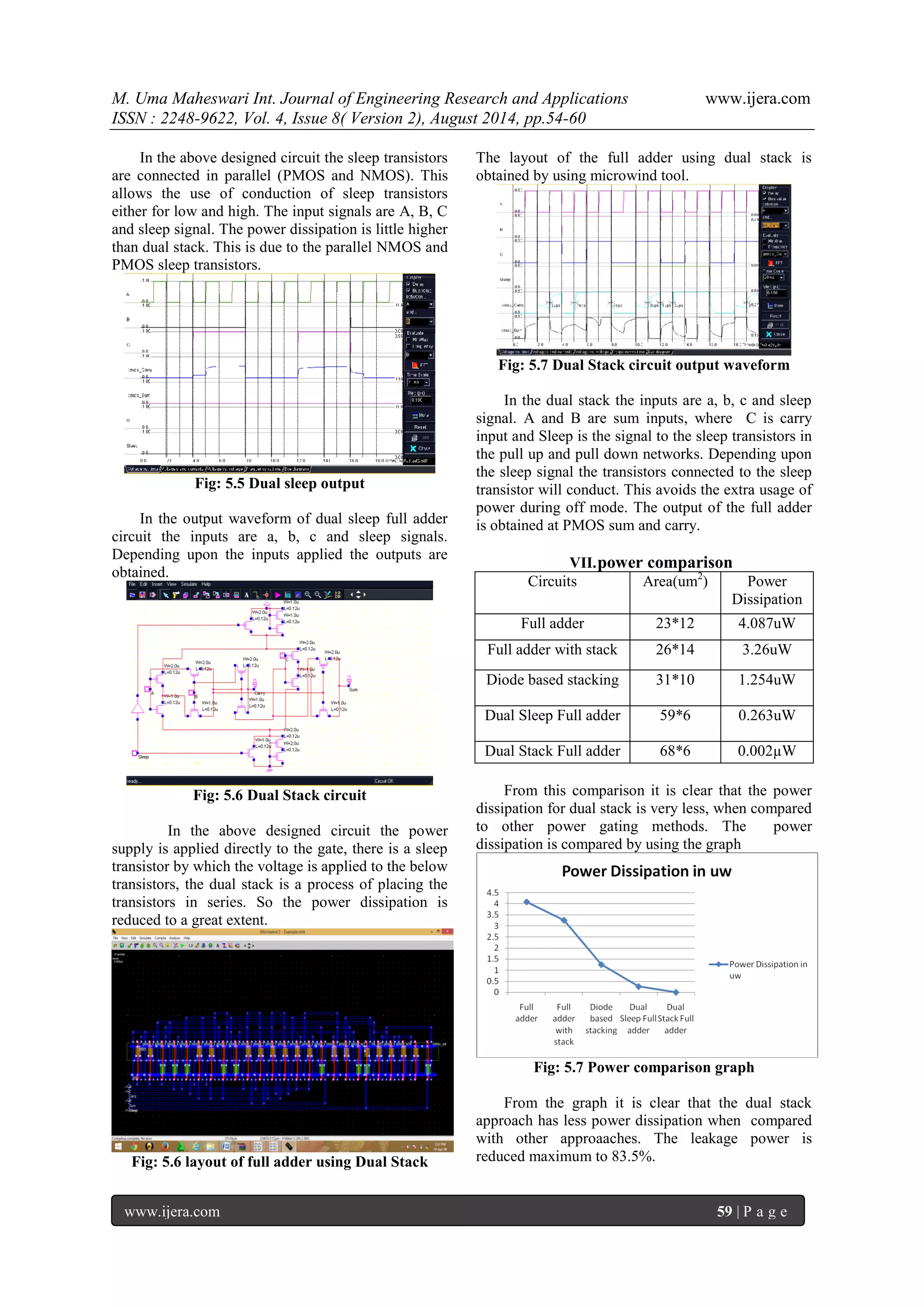
ii) Dual sleep stack approach Fig: 4.2 Dual sleep stack approach Another technique called Dual sleep approach shown in fig: uses the advantage of using the two extra pull-up and two extra pull-down transistors in sleep mode either in OFF state or in ON state. Since the dual sleep portion can be made common to all logic circuitry, less number of transistors is needed to apply a certain logic circuit.
iii) Sleepy approach
In the sleep approach, a "sleep" PMOS transistor is placed between Vdd and the pull-up network of a circuit and a "sleep" NMOS transistor is placed between the pull-down network and Gnd. These sleep transistors turn off the circuit by cutting off the power rails. The sleep transistors are turned on when the circuit is active and turned off when the circuit is idle. By cutting off the power source, this technique can reduce leakage power effectively. However, output will be floating after sleep mode, so the technique results in destruction of state plus a floating output voltage. Fig: 4.3 Sleep approach
iv) Sleepy keeper
In this leakage reduction technique, which is called as the “sleepy keeper” approach? This section explains the structure of the sleepy keeper approach as well as how it operates. In addition, some layout issues for the sleepy keeper approach. The basic problem with traditional CMOS is that the transistors are used only in their most efficient, and naturally inverting, way: namely, PMOS transistors connect to
5. M. Uma Maheswari Int. Journal of Engineering Research and Applications www.ijera.com
ISSN : 2248-9622, Vol. 4, Issue 8( Version 2), August 2014, pp.54-60
www.ijera.com 58 | P a g e
VDD and NMOS transistors connect to GND. It is well known that PMOS transistors are not efficient at passing GND; similarly, it is well known that NMOS transistors are not efficient at passing VDD. Fig: 4.4 Sleepy keeper approach
V. Dual stack
The dual stack method has noise efficiency & power efficiency than normal full adders. Dual stack technique that reduces not only leakage power but also dynamic power. Here the use of two PMOS in the pull-down network and two NMOS in the pull up Network. The advantage is that NMOS degrades the high logic level while PMOS degrades the low logic level. Due to the body effect, they further decrease the voltage level. Fig: 4.5 Dual stack approach So, the pass transistors decreases the voltage applied across the main circuit. As the static power is proportional to the voltage applied, with the reduced voltage the power decreases but there is the advantage of state retention [10].
VI. Results
Any CMOS circuits can be designed by implementing the power gating. The full adder has been designed as shown in below figures Fig: 5.1 Full adder schematic The above designed schematic is full adder using CMOS transistors. This circuit has some leakage power when no input is given. The layout of the designed circuit is shown in figure 5.2. Fig: 5.2 Full adder layout The layout of the full adder is obtained by using microwind tool. Fig: 5.3 Full adder waveform The output waveform of full adder is shown in figure 5.3. The total power dissipation is also obtained Fig: 5.4 Dual Sleep Circuit
6. M. Uma Maheswari Int. Journal of Engineering Research and Applications www.ijera.com
ISSN : 2248-9622, Vol. 4, Issue 8( Version 2), August 2014, pp.54-60
www.ijera.com 59 | P a g e
In the above designed circuit the sleep transistors are connected in parallel (PMOS and NMOS). This allows the use of conduction of sleep transistors either for low and high. The input signals are A, B, C and sleep signal. The power dissipation is little higher than dual stack. This is due to the parallel NMOS and PMOS sleep transistors. Fig: 5.5 Dual sleep output In the output waveform of dual sleep full adder circuit the inputs are a, b, c and sleep signals. Depending upon the inputs applied the outputs are obtained. Fig: 5.6 Dual Stack circuit In the above designed circuit the power supply is applied directly to the gate, there is a sleep transistor by which the voltage is applied to the below transistors, the dual stack is a process of placing the transistors in series. So the power dissipation is reduced to a great extent. Fig: 5.6 layout of full adder using Dual Stack
The layout of the full adder using dual stack is obtained by using microwind tool. Fig: 5.7 Dual Stack circuit output waveform In the dual stack the inputs are a, b, c and sleep signal. A and B are sum inputs, where C is carry input and Sleep is the signal to the sleep transistors in the pull up and pull down networks. Depending upon the sleep signal the transistors connected to the sleep transistor will conduct. This avoids the extra usage of power during off mode. The output of the full adder is obtained at PMOS sum and carry.
VII. power comparison
Circuits
Area(um2)
Power Dissipation
Full adder
23*12
4.087uW
Full adder with stack
26*14
3.26uW
Diode based stacking
31*10
1.254uW
Dual Sleep Full adder
59*6
0.263uW
Dual Stack Full adder
68*6
0.002μW
From this comparison it is clear that the power dissipation for dual stack is very less, when compared to other power gating methods. The power dissipation is compared by using the graph Fig: 5.7 Power comparison graph From the graph it is clear that the dual stack approach has less power dissipation when compared with other approaaches. The leakage power is reduced maximum to 83.5%.
7. M. Uma Maheswari Int. Journal of Engineering Research and Applications www.ijera.com
ISSN : 2248-9622, Vol. 4, Issue 8( Version 2), August 2014, pp.54-60
www.ijera.com 60 | P a g e
VIII. Conclusion
In nanometer scale CMOS technology, although previous approaches are effective in some ways, no perfect solution for reducing leakage power consumption is yet known. Therefore, designers choose techniques based upon technology and design criteria. In this paper, a novel circuit structure named “Dual stack” as a new remedy for designer in terms of static power and dynamic powers. Unlike the sleep transistor technique, the dual stack technique retains the original state. The dual stack approach shows the least speed power product among all methods. Therefore, the dual stack technique provides new ways to designers who require ultra-low leakage power consumption with much less speed power product. Especially it shows nearly 50-80% of power than the existing normal or conventional full adders. So, it can be used for future integrated circuits for power & area efficiency. REFERENCES [1] Shilpi Birla, Neeraj K. Shukla, Manisha Pattanaik and R. K Singh "Analysisof the data stability and leakage reduction in the various SRAM cells topologies", International Journal of engineering science & technology computer (HEST), Singapore, vol. 2(7), 2010, pp. 2936-2944, ISSN: 0975- 5462. [2] M. Tie, H. Dong, T. Wong, Xu Cheng, " Dual- Vth leakage reduction with fast clock skew scheduling enhancement", IEEE conference on Design Automation & Test in Europe, 2010, pp. 520-525. [3] R Bhanuprakash, Manisha Pattanaik, S.S Rajput and Kaushik Mazumdar, "Analysis & reduction of ground bounce noise and leakage current during mode transition of stacking power gating logic circuits" , proceedings of IEEE TENCON Singapore, pp. 1-6, 2009. [4] Shilpi Birla, Neeraj Kr. Shukla, RK Singh and Manisha Pattanaik, " Device and circuit design challenges for low leakage SRAM for ultra low power applications", Canadian Journal of Electrical and Electronics Engineering (EEE) Canada, USA, voU, no.7, Dec. 2010, pp. 156-157, ISSN: I 923- 0540. [5] M. H. Chowdhary, G. Gjanc, J.P. Khaled, "Controlling ground bounce noise in power gating scheme for system- on- chip," in Proc. Int. Symposium on VLSI (2008), pp. 437- 440.
[6] J. Park, “Sleepy Stack: a New Approach to Low Power VLSI and Memory,” Ph.D. Dissertation, School of Electrical and Computer Engineering, Georgia Institute of Technology, 2005. [Online].Available http://etd.gatech.edu/theses.
[7] S. Mutoh, T. Douseki,. Y. Matsuya, T. Aoki, S. Shigemitsu and J. Yamada, “1-V Power Supply High-speed Digital Circuit Technology with Multithreshold-Voltage CMOS,” IEEE Journal of Solis-State Circuits, vol. 30, no. 8, pp. 847–854, August 1995. [8] N. Kim, T. Austin, D. Baauw, T. Mudge, K. Flautner, J. Hu, M. Irwin, M. Kandemir and V. Narayanan, “Leakage Current: Moore’s Law Meets Static Power,” IEEE Computer, vol. 36, pp. 68–75, December 2003. [9] K.-S. Min, H. Kawaguchi and T. Sakurai, “Zigzag Super Cut-off CMOS (ZSCCMOS) Block Activation with Self-Adaptive Voltage Level Controller: An Alternative to Clock- gating Scheme in Leakage. [10] J . Shin and T. Kim, “Technique for transition energy-aware dynamic voltage asNMOS1gnment,” IEEE Trans. Integer. Circuits Syst. II, Exp. Briefs,vol. 53, no. 9, pp. 956–960, Sep. 2006. [11] W. Cheol and T. Kim, “Optimal voltage allocation techniques for dynamically variable voltage processors,” ACM Trans. EmbeddedComput. Syst., vol. 4, no. 1, pp. 211–230, Feb. 2005. [12] T. Ishihara and H. Yasuura, “Voltage scheduling problem for dynamically variable voltage processors,” in Proc. IEEE/ACM Int. Symp. Low Power Electron. Des., 1998, pp. 197–202. [13] F. Fallah and M. Perham, “Standby and active leakage current control and minimization CMOS VLSI circuits,” IEICE Trans. Electron., vol.E88-C, no. 4, pp. 509– 519, 2005. [14] J. Friedrich, B. McCredie, N. James, B. Huott, B. Curran, E. Fluor, G.Mittal, E. Chan, Y. Chan, D. Plass, S. Chu, H. Le, L. Clark, J. Ripley, Taylor, J. Duello, and M. Lanzerotti, “Design of the Power6 microprocessor, ”inProc. IEEE/ACM Int. Solid-State Circuits Conf., Feb. 2007,pp. 96–97. [15] S. Mutoh, T. Douseki, Y. Matsuya, T. Aoki, S. Shigemitsu, and J. Yamada,“1-V power supply high-speed digital circuit technology with multi-threshold voltage CMOS,” IEEE J. Solid-State Circuits, vol. 30, no. 8, pp. 847–854, Aug. 1995.