SlideShare a Scribd company logo
IJSRD - International Journal for Scientific Research & Development| Vol. 3, Issue 10, 2015 | ISSN (online): 2321-0613
All rights reserved by www.ijsrd.com 624
Power Dissipation of VLSI Circuits and Modern Techniques of Designing
Low Power VLSI Systems
Prolay Ghosh
Department of Information Technology
JIS College of Engineering Kalyani, Nadia, West Bengal
Abstract— This paper focus on the various sources of power
dissipation in modern VLSI circuits. This paper also discuss
the importance of designing low power VLSI circuits along
with various techniques of power reduction and its
advantages and disadvantages. It is basically a comparative
study between various power reduction techniques in
modern VLSI circuits.
Key words: Threshold voltage, leakage current, Rise and
Fall time, Activity factor, Operating frequency
I. INTRODUCTION
During the desktop Pc design era VLSI design technique
was much more focused on optimizing speed to execute real
time functions. As a result designers have integrated
semiconductor ICs with various complex signal processing
and graphical processing units but we sacrificed the
portability. Now a day’s portable electronics applications
like tablets, smart phones e.t.c. are rapidly making their way
to consumer electronics market. On other hand more and
more number of transistors are getting added in modern
VLSI chip as the demand of System on Chip (SoC) is
increasing. These increasing features are also leading to high
power dissipation. Consumer demands a portable electronic
device which includes all the features without consuming
much power. So the most important factor to consider while
designing SoC for portable device in ‘low power design’.
Here the cause of power dissipation and the techniques of
power dissipation reduction in discussed.
II. POWER DISSIPATION
Power dissipation has three components:
A. Static Power:
The semiconductor consumes Static power dissipation due
to leakage current. Leakage current is that current which
flows when the ideal current is Zero. The capacitor such as
transistors or diodes conduct a small amount of current even
when they are turned off as capacitor discharges slowly. It
caused some unintended power loss from a capacitor. The
leakage current also generates heat that leads to degraded
performance. It is observed that in deep submicron
technology leakage current contributes 50% of total power
consumption.
Static power dissipation (Pstatic) = Supply Voltage (VDD) *
Leakage Current (Ileakage)
Fig. 1: Leakage Current
Two major components of Leakage current are:
1) Sub threshold leakage:
When the gate voltage is below the threshold voltage current
conducted between source and drain in MOS transistor
caused sub threshold leakage. It can be as high as 80-90% of
total circuit leakage.
2) Gate oxide leakage:
If a high electric field is applied to a MOS transistor with
low oxide thickness then a current flows through the oxide
tunnel is called gate oxide leakage.
Fig. 2: Sub Threshold Leakage and Gate Oxide Leakage
B. Dynamic Capacitive Power:
CMOS digital circuits consume power while charging and
discharging various load capacitances. Dynamic power is
dissipated when energy is drawn from power supply to
charge up the output node capacitance. During this charge
up phase the energy drawn from the power supply is
dissipated as heat in the conducting pMOS transistor. No
energy is drawn from power power supply during charge
down phase, yet the energy stored in the output capacitance
during charge up is dissipated as heat in the conducting
nMOS transistors, as the output voltage drops from VDD to
0.
Power Dissipation of VLSI Circuits and Modern Techniques of Designing Low Power VLSI Systems
(IJSRD/Vol. 3/Issue 10/2015/133)
All rights reserved by www.ijsrd.com 625
Fig. 3: Dynamic Capacitive Power
Pdynamic = load capacitance(CL) * VDD
2
* operating
frequency(Fop)
The dynamic capacitive power dissipation is based
on the assumption that the output node undergoes one
power-consuming transition (0 to VDD) in each clock cycle.
This assumption is not always correct. Depending on the
circuit topology, logic style and the input signal statistics the
node transition rate can be slower than the clock rate. So we
introduce node transition factor or activity factor (α), which
is effective number of power consuming voltage transitions
experienced per clock cycle. It is directly proportional to
dynamic power consumption. So the previously stated
equation of dynamic capacitive power is modified as
Pdynamic = α *CL* VDD
2
* Fop
C. Dynamic Short-Circuit Power:
Short-circuit power, is caused by the short circuit currents
that arise when pairs of pMOS/nMOS transistors are
conducting simultaneously. As the input voltage makes a
transition from logic 0 to 1,ideally pMOS should turned off
and nMOS should turned on. But the process takes small
time till then both the transistors remain on and it provides a
short circuit path from supply voltage to ground.
Short-circuit power (Psc) = VDD * time of slope (Tsc)
*Imax.
Fig. 4: Dynamic Short-Circuit Power
III. POWER DISSIPATION REDUCTION TECHNIQUE
We have discussed various components of power
dissipation. Now we have to think about the power
dissipation reduction technique
A. Static power consumption reduction:
Static power consumption can be reduced if we can reduce
the supply voltage and leakage current.
1) Supply voltage reduction:
Supply voltage has direct relation with power consumption.
Supply voltage of 3.3V is widely used in present days
MOSFET. Experiment has shows that if we can scale down
supply voltage to 1V power consumption will be reduced 10
times as shows in figure 5.
Fig. 5: Supply Voltage Vs Power Consumption
Supply voltage scaling is a god technique to reduce
power consumption it affects the performance of the circuit
as it caused drastic increase in gate delay. So in modern
VLSI circuits we have to maintain a balance between speed
and power.
2) Variation of threshold voltage:
Threshold voltage is defined as the minimum voltage that
required to make the transistor ON. Transistor maybe either
nMOS or pMOS. For nMOS the threshold voltage is
positive and for pMOS threshold voltage is positive.
The threshold voltage ( Vth) of a field effect transistor
(FET) is the value of the gate-source voltage(Vgs) when the
conducting channel just begins to connect the source and
drain contacts of the transistor, allowing significant current
to flow. If Vgs is less than Vth then there will be no current
flow.
Fig. 6: Threshold Voltage
a) Multiple threshold CMOS circuit (MTCMOS):
The new MTCMOS circuit technology is proposed to satisfy
both requirements of lowering the threshold voltage of a
MOSFET and reducing stand-by current, both of which are
necessary to obtain high-speed low-power performance at a
supply voltage of 1V. This technology has two main
features. One is that N-channel and P-channel MOSFET's
Power Dissipation of VLSI Circuits and Modern Techniques of Designing Low Power VLSI Systems
(IJSRD/Vol. 3/Issue 10/2015/133)
All rights reserved by www.ijsrd.com 626
with two different threshold voltages are employed in a
single chip. The other one is two operational modes,
"active" and "sleep," for efficient power management. MOS
transistors with low threshold voltage (Vth) are placed in the
critical path while MOS transistors with high threshold
voltage (Vth), are placed in the non-critical path. In the
critical path gate delay time should be as low as possible.
Hence delay reduction is traded off against leakage by
placing low threshold transistors causing faster gate
transitions. However, in the non timing critical path, high
threshold transistors are placed to reduce leakage as
speed/delay has less importance here. It is observed that in
modern VLSI circuits as used in industry, 80% of the paths
are non-timing critical. Data path can be broadly classified
into two categories Timing Critical and non-Timing Critical.
Here, Critical path means the path having the largest timing
delay.
The logic gate is composed of MOSFET's with a
low threshold voltage of about 0.2-0.3 V. Its power
terminals are not connected directly to the power supply
lines VDD and GND, but rather to the "virtual" power
supply lines VDDV and GNDV. The real and virtual power
lines are linked by MOSFET's QI and Q2. These have a high
threshold voltage of about 0.5-0.6 V and serve as sleep
control transistors. Signals SL and SL, which are connected
to the gates of QI and Q2, respectively, are used for
active/sleep mode control. Circuit operation in each mode at
a supply voltage of 1V is described below.
Fig: 7: Example of Multiple Threshold Voltage CMOS
In the active mode, when SL is set low, QI and Q2
are turned on and their on-resistance is so small that VDDV
and GNDV function as real power lines. Therefore, the
NAND gate operates normally and at a high speed because
the Vth of 0.3 V is low enough relative to the supply voltage
of 1 V. In the sleep mode, when SL is set high, Ql and Q2
are turned off so that the virtual lines VDDV and GNDV are
assumed to be floating. The relatively large leakage current,
determined by the subthreshold characteristics of low-Vth
MOSFET's, is almost completely suppressed by Ql and Q2
since they have a high Vth and thus a much lower leakage
current. Therefore, power consumption during the stand-by
period can be dramatically reduced by the sleep control. It
should be pointed out that two other factors affect the speed
performance of an MTCMOS circuit. One is the size of the
sleep control transistors Ql and Q2, and the other is the
capacitances CV1 and CV2 of the virtual power lines.
b) Variable threshold CMOS circuit (VTCMOS):
In VTCMOS technique the threshold voltage is varied by a
suitable control circuit according to the circuit requirements.
As is evident from the expression above, threshold voltage
is a function of the source to body bias. Hence variation of
this bias voltage using suitable circuitry can vary threshold
voltage. Practically for critical paths threshold voltage is
lowered as switching speed is of primary concern for such
paths. But for non-critical paths threshold voltage is
increased to reduce the leakage power dissipation, as higher
threshold prevents any sort of unwanted leakage power
flow.
VBN=0V are produced for PMOS and NMOS
respectively. Due to this, the circuit has high switching
speed (due to low Vth) at the cost of leakage power. In
standby mode the control circuit generates a lower substrate
voltage for NMOS and higher substrate voltage for PMOS
.This causes the threshold voltage of both the NMOS and
PMOS to increase, thus reducing the leakage current.
Besides changing the supply voltage (VDD) and the threshold
voltage (Vth).
Fig. 8: Example of Variable Threshold Voltage CMOS
3) Dynamic Threshold MOS:
In dynamic threshold CMOS (DTMOS), the threshold
voltage is altered dynamically to suit the operating state of
the circuit. A high threshold voltage in the standby mode
gives low leakage current, while a low threshold voltage
allows for higher current drives in the active mode of
operation. Dynamic threshold CMOS can be achieved by
tying the gate and body together. The supply voltage of
DTMOS is limited by the diode built-in potential in bulk
silicon technology. The pn diode between source and body
should be reverse biased. Hence, this technique is only
suitable for ultralow voltage (0.6V and below) circuits in
bulk CMOS.
Fig. 9: FTCMOS Circuit
Power Dissipation of VLSI Circuits and Modern Techniques of Designing Low Power VLSI Systems
(IJSRD/Vol. 3/Issue 10/2015/133)
All rights reserved by www.ijsrd.com 627
4) Gate Leakage prevention:
In deep sub-micron technology, gate oxide thickness
reached 10-20A0 causing exponential increase in tunneling
current through extremely thin gate oxide. In 45nm
technology, gate leakage got increased by 10 times with
respect to previous process technology. Hence, thicker
insulator is used to reduce gate leakage. Thicker insulator
(increase in Tox) reduces Cox, i.e the gate oxide capacitance
per unit area = (K/Tox, where K= permitivitty of gate oxide)
causing increase in threshold voltage (Vth) and thus
reducing device speed. Hence, to keep Cox constant,
different insulating materials having higher permittivity than
SiO2 is used from 45nm technology onwards. Since
insulating material is changed, polysilicon gate is also
replaced by new metal gate to maintain low work function.
B. Dynamic capacitive power consumption reduction:
Dynamic power dissipation depends on four parameters
namely Load Capacitance (CL), Supply
Voltage (VDD), Activity factor (α) and frequency
(Fop). Their impacts and way of reducing power dissipation
are discussed below.
1) Load Capacitance:
In modern SOC applications, large load capacitance may
appear due to high fanout net or long wire distance between
driver and receiver gate resulting in increase in dynamic
power dissipation.
a) Reduction Technique:
To improve power performance down sizing driver and
receiver gate is popular technique. By downsizing a
transistor, the design can be more compact. Proper
placement androuting is also necessary so that the length of
the wire can be minimized to reduce load capacitance.
Decreasing Capacitance is also difficult as it need to scale
down the device and wiring.
2) Activity factor:
The toggling rate of a signal with respect to clock is termed
as Activity factor (α). Dynamic power dissipation is directly
proportional to α.
a) Reduction Technique:
To reduce Activity factor, most popular technique used in
industry is Clock Gating. In this method, the clock signal to
different functional block is gated by enabling signals. In
most cases, AND gates are preferred for gating clock
signals.
Fig. 10: Clock Gating
The above diagram illustrates the concept of clock
gating. When ENABLE=1, clock can be applied to
functional block through AND gate. However to avoid
unnecessary switching when the functional block is inactive,
the ENABLE input can be made 0 so as to disable the clock
propagation when not required. This causes the clock to
become totally inactive when the functional block is in
nonactive mode, thus eliminating any sort of activity in the
circuit. Clock Gating can reduce power leak dueto dynamic
power by as high as 70 to 80%.
3) Operating frequency:
Sometime higher frequency is needed for better performance
but it causes high power consumption. Introducing parallel
processing lower frequency can be obtained but it increases
Hardware overhead and requires extrusive change at an
architecture or algorithm design.
C. Dynamic Short-Circuit power consumption education:
Dynamic power dissipation depends on two parameters
namely Time of the slope(TSC), Supply Voltage (VDD).
1) Time of the slope(TSC):
Tsc is the duration of the slope of the input signal. This
component is directly depended on the Rise time and Fall
time.
TSC=(TR+TF)2
we can say that fast Rise time, Fall time on input
signal means lower short circuit power dissipation.
Fig. 11: Rise and Fall Time
The Rise time and the Fall time should be small
compared to the clock period. Very large Rise time and fall
time have the risk of the cycles going undetected. Large
Rise and Fall time mean that the signal will be hovering
around mid level for too long making the system highly
susceptible to noise and multiple triggering if there is not
enough hysteresis.
a) Reduction technique:
Rise and Fall time can be reduced by reducing the gate
length of the MOSFET. Strained silicon MOSFET has also
less rise and fall time than bulk sislicon MOSFET. As
electrons can move 70% faster allowing strained silicon
transistors to switch 5% faster.
- The short circuit power can also be reduced by
1) device size reduction and
2) Increasing threshold voltage
Both of which is also used for leakage reduction. In
addition, the input rise and fall times for a digital gate needs
to be less than an upper limit which can be taken care of
during gate sizing. It is important to note that short circuit
power dissipation happens only during switching (Dynamic
power dissipation). Hence reduction of Activity factor (α)
helps both power reductions simultaneously.
Power Dissipation of VLSI Circuits and Modern Techniques of Designing Low Power VLSI Systems
(IJSRD/Vol. 3/Issue 10/2015/133)
All rights reserved by www.ijsrd.com 628
IV. CONCLUSION
The increasing prominence of portable systems and the need
to limit power consumption in very high density ULSI chips
have led to rapid and innovative developments in low power
design during the recent years. Through above discussion
we get a overview about various power dissipation of any
type VLSI circuit and their components. In modern VLSI
circuits separate power management circuits are integrated
for power distribution. As power dissipation reduction has
become a matter of serious concern, various power
reduction techniques are being used. A lots of researches are
also going on this topic. In this paper some ideas of modern
power reductions have been discussed elaborately.
REFERENCES
[1] Fundamentals of semiconductor device ECE 515,
March 5, 2003 Hernando Valencia & Farrin Hockett.
[2] 1-V power supply high speed digital circuit technology
with multi threshold voltage CMOS Shin’ichiro
Mutoh, Takakuni Douseki,Yqsuyuki Matsuya,
Takahko Aoki, Satoshi Shigematsu and Junjo
Yamada,Member IEEE
[3] Low power design by G.Friedman, University of
Rochester
[4] New design methodologies for High speed low power
XOR-XNOR circuits Shiv shankar Mishra, S. Wairya,
R.K.Nagaria and S.Tiwari
[5] Study the amalysys of Low power and High speed
CMOS Logic Circuit in 90nm Technology Fazal
Noorbashar, Ashis verma,A.M.Mahajan
[6] Design Techniques for Low-Voltage High-Speed
Digital Bipolar Circuits Behzad Razavi, Yusuke Ota,
and Robert G. Swartz,Fellow, IEEE
[7] Low Power and High Speed Multi Threshold Voltage
Interface Circuits Sherif A. Tawfik and Volkan
Kursun, Member, IEEE
[8] Low-voltage low-power CMOS full adder,
D.Radhakrishnan
[9] The Effect of gate length on SOI-MOSFETs operation
J.Baedi, and H.Arabshahi
[10]Channel length scaling and the impact of metal gate
work function on the performance of double gate-metal
oxide semiconductor field-effect Transistors D
RECHEM, S LATRECHE and C GONTRAND
[11]Gate-Length Biasing for Runtime-Leakage Control
Puneet Gupta, Puneet Sharma
[12]Supply and Threshold VoltageScaling for Low Power
CMOS Ricardo Gonzalez, Benjamin M. Gordon, and
Mark A. Horowitz.
[13]POWER REDUCTION IN MODERN VLSI
CIRCUITS – A REVIEW Debopam Ghosh, Jyotirmoy
Guha, Arka De, Anirban Mukherjee, Electronics and
Communication Engineering Heritage Institute of
Technology Kolkata, India
[14]Novel Ultra Low Power Multi-threshold CMOS
Technology P.Sreenivasulu1, JNTU Kakinada,
G.Vinatha,DECS,Marakapur Dr. K.Srinivasa
Rao,T.R.R College of Engg, Dr. A.Vinaya
babu,Principal of JNTU College of Eng.
[15]Variable Threshold Voltage CMOS (VTCMOS) in
Series Connected Circuits, Takashi Inukai, Institute of
Industrial Science, University of Tokyo, Japan Toshiro
Hiramoto, Tak VLSI Design and Education Center,
University of Tokyo ayasu Sakurai, Center for
Collaborative Research, University of Tokyo.

More Related Content

What's hot

Lecture21
Lecture21Lecture21
Lecture21
Dharmesh Goyal
 
45nm transistor properties
45nm transistor properties45nm transistor properties
45nm transistor propertiesDeiptii Das
 
Fpga architectures and applications
Fpga architectures and applicationsFpga architectures and applications
Fpga architectures and applications
Sudhanshu Janwadkar
 
Metastability
MetastabilityMetastability
Metastability
Nallapati Anindra
 
Phase-locked Loops - Theory and Design
Phase-locked Loops - Theory and DesignPhase-locked Loops - Theory and Design
Phase-locked Loops - Theory and Design
Simen Li
 
Advanced Low Power Techniques in Chip Design
Advanced Low Power Techniques in Chip DesignAdvanced Low Power Techniques in Chip Design
Advanced Low Power Techniques in Chip Design
Dr. Shivananda Koteshwar
 
Phase locked loop
Phase locked loopPhase locked loop
Phase locked loop
Preet_patel
 
Mos transistor theory
Mos transistor theoryMos transistor theory
Mos transistor theory
Ekta Jolly
 
Synchronous and asynchronous clock
Synchronous and asynchronous clockSynchronous and asynchronous clock
Synchronous and asynchronous clock
Nallapati Anindra
 
Design and development of carry select adder
Design and development of carry select adderDesign and development of carry select adder
Design and development of carry select adder
ABIN THOMAS
 
Unit 3
Unit 3Unit 3
Divide by N clock
Divide by N clockDivide by N clock
Divide by N clock
Mantra VLSI
 
CMOS VLSI design
CMOS VLSI designCMOS VLSI design
CMOS VLSI designRajan Kumar
 
IIR filter realization using direct form I & II
IIR filter realization using direct form I & IIIIR filter realization using direct form I & II
IIR filter realization using direct form I & II
Sarang Joshi
 
Device isolation Techniques
Device isolation TechniquesDevice isolation Techniques
Device isolation Techniques
Sudhanshu Janwadkar
 
Rc delay modelling in vlsi
Rc delay modelling in vlsiRc delay modelling in vlsi
Rc delay modelling in vlsi
Dr. Vishal Sharma
 
STA vs DTA.pptx
STA vs DTA.pptxSTA vs DTA.pptx
STA vs DTA.pptx
Payal Dwivedi
 

What's hot (20)

Lecture21
Lecture21Lecture21
Lecture21
 
45nm transistor properties
45nm transistor properties45nm transistor properties
45nm transistor properties
 
Fpga architectures and applications
Fpga architectures and applicationsFpga architectures and applications
Fpga architectures and applications
 
Metastability
MetastabilityMetastability
Metastability
 
BGR
BGRBGR
BGR
 
Phase-locked Loops - Theory and Design
Phase-locked Loops - Theory and DesignPhase-locked Loops - Theory and Design
Phase-locked Loops - Theory and Design
 
Advanced Low Power Techniques in Chip Design
Advanced Low Power Techniques in Chip DesignAdvanced Low Power Techniques in Chip Design
Advanced Low Power Techniques in Chip Design
 
Phase locked loop
Phase locked loopPhase locked loop
Phase locked loop
 
Mos transistor theory
Mos transistor theoryMos transistor theory
Mos transistor theory
 
Synchronous and asynchronous clock
Synchronous and asynchronous clockSynchronous and asynchronous clock
Synchronous and asynchronous clock
 
Design and development of carry select adder
Design and development of carry select adderDesign and development of carry select adder
Design and development of carry select adder
 
Unit 3
Unit 3Unit 3
Unit 3
 
Divide by N clock
Divide by N clockDivide by N clock
Divide by N clock
 
CMOS VLSI design
CMOS VLSI designCMOS VLSI design
CMOS VLSI design
 
IIR filter realization using direct form I & II
IIR filter realization using direct form I & IIIIR filter realization using direct form I & II
IIR filter realization using direct form I & II
 
Device isolation Techniques
Device isolation TechniquesDevice isolation Techniques
Device isolation Techniques
 
Rc delay modelling in vlsi
Rc delay modelling in vlsiRc delay modelling in vlsi
Rc delay modelling in vlsi
 
Booth Multiplier
Booth MultiplierBooth Multiplier
Booth Multiplier
 
Non ideal effects of pll
Non ideal effects of pllNon ideal effects of pll
Non ideal effects of pll
 
STA vs DTA.pptx
STA vs DTA.pptxSTA vs DTA.pptx
STA vs DTA.pptx
 

Similar to Power Dissipation of VLSI Circuits and Modern Techniques of Designing Low Power VLSI Systems

Design of Memory Cell for Low Power Applications
Design of Memory Cell for Low Power ApplicationsDesign of Memory Cell for Low Power Applications
Design of Memory Cell for Low Power Applications
IJERA Editor
 
Ji3516041608
Ji3516041608Ji3516041608
Ji3516041608
IJERA Editor
 
Sub-Threshold Leakage Current Reduction Techniques In VLSI Circuits -A Survey
Sub-Threshold Leakage Current Reduction Techniques In VLSI Circuits -A SurveySub-Threshold Leakage Current Reduction Techniques In VLSI Circuits -A Survey
Sub-Threshold Leakage Current Reduction Techniques In VLSI Circuits -A Survey
IJERA Editor
 
NOVEL SLEEP TRANSISTOR TECHNIQUES FOR LOW LEAKAGE POWER PERIPHERAL CIRCUITS
NOVEL SLEEP TRANSISTOR TECHNIQUES FOR LOW LEAKAGE POWER PERIPHERAL CIRCUITSNOVEL SLEEP TRANSISTOR TECHNIQUES FOR LOW LEAKAGE POWER PERIPHERAL CIRCUITS
NOVEL SLEEP TRANSISTOR TECHNIQUES FOR LOW LEAKAGE POWER PERIPHERAL CIRCUITS
VLSICS Design
 
NOVEL SLEEP TRANSISTOR TECHNIQUES FOR LOW LEAKAGE POWER PERIPHERAL CIRCUITS
NOVEL SLEEP TRANSISTOR TECHNIQUES FOR LOW LEAKAGE POWER PERIPHERAL CIRCUITSNOVEL SLEEP TRANSISTOR TECHNIQUES FOR LOW LEAKAGE POWER PERIPHERAL CIRCUITS
NOVEL SLEEP TRANSISTOR TECHNIQUES FOR LOW LEAKAGE POWER PERIPHERAL CIRCUITS
VLSICS Design
 
Bc36330333
Bc36330333Bc36330333
Bc36330333
IJERA Editor
 
Analysis, Design and Investigation on a New Single-Phase Switched Quasi Z-Sou...
Analysis, Design and Investigation on a New Single-Phase Switched Quasi Z-Sou...Analysis, Design and Investigation on a New Single-Phase Switched Quasi Z-Sou...
Analysis, Design and Investigation on a New Single-Phase Switched Quasi Z-Sou...
International Journal of Power Electronics and Drive Systems
 
POWER CONSUMPTION AT CIRCUIT OR LOGIC LEVEL IN CIRCUIT
POWER CONSUMPTION AT CIRCUIT OR LOGIC LEVEL IN CIRCUITPOWER CONSUMPTION AT CIRCUIT OR LOGIC LEVEL IN CIRCUIT
POWER CONSUMPTION AT CIRCUIT OR LOGIC LEVEL IN CIRCUIT
Anil Yadav
 
LowPower-VLSI-Unit1.pdf
LowPower-VLSI-Unit1.pdfLowPower-VLSI-Unit1.pdf
LowPower-VLSI-Unit1.pdf
ssuser284b751
 
8LowPowerVLSI THIRD MODULE 2019 SCHEME.pdf
8LowPowerVLSI THIRD MODULE 2019 SCHEME.pdf8LowPowerVLSI THIRD MODULE 2019 SCHEME.pdf
8LowPowerVLSI THIRD MODULE 2019 SCHEME.pdf
RintuKurian3
 
Cp4201612617
Cp4201612617Cp4201612617
Cp4201612617
IJERA Editor
 
Power Gating Based Ground Bounce Noise Reduction
Power Gating Based Ground Bounce Noise ReductionPower Gating Based Ground Bounce Noise Reduction
Power Gating Based Ground Bounce Noise Reduction
IJERA Editor
 
Power consumption
Power consumptionPower consumption
Power consumption
sdpable
 
STAND-BY LEAKAGE POWER REDUCTION IN NANOSCALE STATIC CMOS VLSI MULTIPLIER CIR...
STAND-BY LEAKAGE POWER REDUCTION IN NANOSCALE STATIC CMOS VLSI MULTIPLIER CIR...STAND-BY LEAKAGE POWER REDUCTION IN NANOSCALE STATIC CMOS VLSI MULTIPLIER CIR...
STAND-BY LEAKAGE POWER REDUCTION IN NANOSCALE STATIC CMOS VLSI MULTIPLIER CIR...
VLSICS Design
 
Design of 64 bit SRAM using Lector Technique for Low Leakage Power with Read ...
Design of 64 bit SRAM using Lector Technique for Low Leakage Power with Read ...Design of 64 bit SRAM using Lector Technique for Low Leakage Power with Read ...
Design of 64 bit SRAM using Lector Technique for Low Leakage Power with Read ...
IOSRJVSP
 
A novel approach for leakage power reduction techniques in 65nm technologies
A novel approach for leakage power reduction techniques in 65nm technologiesA novel approach for leakage power reduction techniques in 65nm technologies
A novel approach for leakage power reduction techniques in 65nm technologies
VLSICS Design
 
A NOVEL APPROACH FOR LEAKAGE POWER REDUCTION TECHNIQUES IN 65NM TECHNOLOGIES
A NOVEL APPROACH FOR LEAKAGE POWER REDUCTION TECHNIQUES IN 65NM TECHNOLOGIESA NOVEL APPROACH FOR LEAKAGE POWER REDUCTION TECHNIQUES IN 65NM TECHNOLOGIES
A NOVEL APPROACH FOR LEAKAGE POWER REDUCTION TECHNIQUES IN 65NM TECHNOLOGIES
VLSICS Design
 
Low power 6 transistor latch design for portable devices
Low power 6 transistor latch design for portable devicesLow power 6 transistor latch design for portable devices
Low power 6 transistor latch design for portable devices
Alexander Decker
 
Leakage Power Reduction Techniques Revisited in a CMOS Inverter Circuit at De...
Leakage Power Reduction Techniques Revisited in a CMOS Inverter Circuit at De...Leakage Power Reduction Techniques Revisited in a CMOS Inverter Circuit at De...
Leakage Power Reduction Techniques Revisited in a CMOS Inverter Circuit at De...
idescitation
 

Similar to Power Dissipation of VLSI Circuits and Modern Techniques of Designing Low Power VLSI Systems (20)

Design of Memory Cell for Low Power Applications
Design of Memory Cell for Low Power ApplicationsDesign of Memory Cell for Low Power Applications
Design of Memory Cell for Low Power Applications
 
Ji3516041608
Ji3516041608Ji3516041608
Ji3516041608
 
Sub-Threshold Leakage Current Reduction Techniques In VLSI Circuits -A Survey
Sub-Threshold Leakage Current Reduction Techniques In VLSI Circuits -A SurveySub-Threshold Leakage Current Reduction Techniques In VLSI Circuits -A Survey
Sub-Threshold Leakage Current Reduction Techniques In VLSI Circuits -A Survey
 
NOVEL SLEEP TRANSISTOR TECHNIQUES FOR LOW LEAKAGE POWER PERIPHERAL CIRCUITS
NOVEL SLEEP TRANSISTOR TECHNIQUES FOR LOW LEAKAGE POWER PERIPHERAL CIRCUITSNOVEL SLEEP TRANSISTOR TECHNIQUES FOR LOW LEAKAGE POWER PERIPHERAL CIRCUITS
NOVEL SLEEP TRANSISTOR TECHNIQUES FOR LOW LEAKAGE POWER PERIPHERAL CIRCUITS
 
NOVEL SLEEP TRANSISTOR TECHNIQUES FOR LOW LEAKAGE POWER PERIPHERAL CIRCUITS
NOVEL SLEEP TRANSISTOR TECHNIQUES FOR LOW LEAKAGE POWER PERIPHERAL CIRCUITSNOVEL SLEEP TRANSISTOR TECHNIQUES FOR LOW LEAKAGE POWER PERIPHERAL CIRCUITS
NOVEL SLEEP TRANSISTOR TECHNIQUES FOR LOW LEAKAGE POWER PERIPHERAL CIRCUITS
 
Bg26386390
Bg26386390Bg26386390
Bg26386390
 
Bc36330333
Bc36330333Bc36330333
Bc36330333
 
Analysis, Design and Investigation on a New Single-Phase Switched Quasi Z-Sou...
Analysis, Design and Investigation on a New Single-Phase Switched Quasi Z-Sou...Analysis, Design and Investigation on a New Single-Phase Switched Quasi Z-Sou...
Analysis, Design and Investigation on a New Single-Phase Switched Quasi Z-Sou...
 
POWER CONSUMPTION AT CIRCUIT OR LOGIC LEVEL IN CIRCUIT
POWER CONSUMPTION AT CIRCUIT OR LOGIC LEVEL IN CIRCUITPOWER CONSUMPTION AT CIRCUIT OR LOGIC LEVEL IN CIRCUIT
POWER CONSUMPTION AT CIRCUIT OR LOGIC LEVEL IN CIRCUIT
 
LowPower-VLSI-Unit1.pdf
LowPower-VLSI-Unit1.pdfLowPower-VLSI-Unit1.pdf
LowPower-VLSI-Unit1.pdf
 
8LowPowerVLSI THIRD MODULE 2019 SCHEME.pdf
8LowPowerVLSI THIRD MODULE 2019 SCHEME.pdf8LowPowerVLSI THIRD MODULE 2019 SCHEME.pdf
8LowPowerVLSI THIRD MODULE 2019 SCHEME.pdf
 
Cp4201612617
Cp4201612617Cp4201612617
Cp4201612617
 
Power Gating Based Ground Bounce Noise Reduction
Power Gating Based Ground Bounce Noise ReductionPower Gating Based Ground Bounce Noise Reduction
Power Gating Based Ground Bounce Noise Reduction
 
Power consumption
Power consumptionPower consumption
Power consumption
 
STAND-BY LEAKAGE POWER REDUCTION IN NANOSCALE STATIC CMOS VLSI MULTIPLIER CIR...
STAND-BY LEAKAGE POWER REDUCTION IN NANOSCALE STATIC CMOS VLSI MULTIPLIER CIR...STAND-BY LEAKAGE POWER REDUCTION IN NANOSCALE STATIC CMOS VLSI MULTIPLIER CIR...
STAND-BY LEAKAGE POWER REDUCTION IN NANOSCALE STATIC CMOS VLSI MULTIPLIER CIR...
 
Design of 64 bit SRAM using Lector Technique for Low Leakage Power with Read ...
Design of 64 bit SRAM using Lector Technique for Low Leakage Power with Read ...Design of 64 bit SRAM using Lector Technique for Low Leakage Power with Read ...
Design of 64 bit SRAM using Lector Technique for Low Leakage Power with Read ...
 
A novel approach for leakage power reduction techniques in 65nm technologies
A novel approach for leakage power reduction techniques in 65nm technologiesA novel approach for leakage power reduction techniques in 65nm technologies
A novel approach for leakage power reduction techniques in 65nm technologies
 
A NOVEL APPROACH FOR LEAKAGE POWER REDUCTION TECHNIQUES IN 65NM TECHNOLOGIES
A NOVEL APPROACH FOR LEAKAGE POWER REDUCTION TECHNIQUES IN 65NM TECHNOLOGIESA NOVEL APPROACH FOR LEAKAGE POWER REDUCTION TECHNIQUES IN 65NM TECHNOLOGIES
A NOVEL APPROACH FOR LEAKAGE POWER REDUCTION TECHNIQUES IN 65NM TECHNOLOGIES
 
Low power 6 transistor latch design for portable devices
Low power 6 transistor latch design for portable devicesLow power 6 transistor latch design for portable devices
Low power 6 transistor latch design for portable devices
 
Leakage Power Reduction Techniques Revisited in a CMOS Inverter Circuit at De...
Leakage Power Reduction Techniques Revisited in a CMOS Inverter Circuit at De...Leakage Power Reduction Techniques Revisited in a CMOS Inverter Circuit at De...
Leakage Power Reduction Techniques Revisited in a CMOS Inverter Circuit at De...
 

More from IJSRD

#IJSRD #Research Paper Publication
#IJSRD #Research Paper Publication#IJSRD #Research Paper Publication
#IJSRD #Research Paper Publication
IJSRD
 
Maintaining Data Confidentiality in Association Rule Mining in Distributed En...
Maintaining Data Confidentiality in Association Rule Mining in Distributed En...Maintaining Data Confidentiality in Association Rule Mining in Distributed En...
Maintaining Data Confidentiality in Association Rule Mining in Distributed En...
IJSRD
 
Performance and Emission characteristics of a Single Cylinder Four Stroke Die...
Performance and Emission characteristics of a Single Cylinder Four Stroke Die...Performance and Emission characteristics of a Single Cylinder Four Stroke Die...
Performance and Emission characteristics of a Single Cylinder Four Stroke Die...
IJSRD
 
Preclusion of High and Low Pressure In Boiler by Using LABVIEW
Preclusion of High and Low Pressure In Boiler by Using LABVIEWPreclusion of High and Low Pressure In Boiler by Using LABVIEW
Preclusion of High and Low Pressure In Boiler by Using LABVIEW
IJSRD
 
Prevention and Detection of Man in the Middle Attack on AODV Protocol
Prevention and Detection of Man in the Middle Attack on AODV ProtocolPrevention and Detection of Man in the Middle Attack on AODV Protocol
Prevention and Detection of Man in the Middle Attack on AODV Protocol
IJSRD
 
Comparative Analysis of PAPR Reduction Techniques in OFDM Using Precoding Tec...
Comparative Analysis of PAPR Reduction Techniques in OFDM Using Precoding Tec...Comparative Analysis of PAPR Reduction Techniques in OFDM Using Precoding Tec...
Comparative Analysis of PAPR Reduction Techniques in OFDM Using Precoding Tec...
IJSRD
 
Evaluation the Effect of Machining Parameters on MRR of Mild Steel
Evaluation the Effect of Machining Parameters on MRR of Mild SteelEvaluation the Effect of Machining Parameters on MRR of Mild Steel
Evaluation the Effect of Machining Parameters on MRR of Mild Steel
IJSRD
 
Filter unwanted messages from walls and blocking nonlegitimate user in osn
Filter unwanted messages from walls and blocking nonlegitimate user in osnFilter unwanted messages from walls and blocking nonlegitimate user in osn
Filter unwanted messages from walls and blocking nonlegitimate user in osn
IJSRD
 
Keystroke Dynamics Authentication with Project Management System
Keystroke Dynamics Authentication with Project Management SystemKeystroke Dynamics Authentication with Project Management System
Keystroke Dynamics Authentication with Project Management System
IJSRD
 
Diagnosing lungs cancer Using Neural Networks
Diagnosing lungs cancer Using Neural NetworksDiagnosing lungs cancer Using Neural Networks
Diagnosing lungs cancer Using Neural Networks
IJSRD
 
A Survey on Sentiment Analysis and Opinion Mining
A Survey on Sentiment Analysis and Opinion MiningA Survey on Sentiment Analysis and Opinion Mining
A Survey on Sentiment Analysis and Opinion Mining
IJSRD
 
A Defect Prediction Model for Software Product based on ANFIS
A Defect Prediction Model for Software Product based on ANFISA Defect Prediction Model for Software Product based on ANFIS
A Defect Prediction Model for Software Product based on ANFIS
IJSRD
 
Experimental Investigation of Granulated Blast Furnace Slag ond Quarry Dust a...
Experimental Investigation of Granulated Blast Furnace Slag ond Quarry Dust a...Experimental Investigation of Granulated Blast Furnace Slag ond Quarry Dust a...
Experimental Investigation of Granulated Blast Furnace Slag ond Quarry Dust a...
IJSRD
 
Product Quality Analysis based on online Reviews
Product Quality Analysis based on online ReviewsProduct Quality Analysis based on online Reviews
Product Quality Analysis based on online Reviews
IJSRD
 
Solving Fuzzy Matrix Games Defuzzificated by Trapezoidal Parabolic Fuzzy Numbers
Solving Fuzzy Matrix Games Defuzzificated by Trapezoidal Parabolic Fuzzy NumbersSolving Fuzzy Matrix Games Defuzzificated by Trapezoidal Parabolic Fuzzy Numbers
Solving Fuzzy Matrix Games Defuzzificated by Trapezoidal Parabolic Fuzzy Numbers
IJSRD
 
Study of Clustering of Data Base in Education Sector Using Data Mining
Study of Clustering of Data Base in Education Sector Using Data MiningStudy of Clustering of Data Base in Education Sector Using Data Mining
Study of Clustering of Data Base in Education Sector Using Data Mining
IJSRD
 
Fault Tolerance in Big Data Processing Using Heartbeat Messages and Data Repl...
Fault Tolerance in Big Data Processing Using Heartbeat Messages and Data Repl...Fault Tolerance in Big Data Processing Using Heartbeat Messages and Data Repl...
Fault Tolerance in Big Data Processing Using Heartbeat Messages and Data Repl...
IJSRD
 
Investigation of Effect of Process Parameters on Maximum Temperature during F...
Investigation of Effect of Process Parameters on Maximum Temperature during F...Investigation of Effect of Process Parameters on Maximum Temperature during F...
Investigation of Effect of Process Parameters on Maximum Temperature during F...
IJSRD
 
Review Paper on Computer Aided Design & Analysis of Rotor Shaft of a Rotavator
Review Paper on Computer Aided Design & Analysis of Rotor Shaft of a RotavatorReview Paper on Computer Aided Design & Analysis of Rotor Shaft of a Rotavator
Review Paper on Computer Aided Design & Analysis of Rotor Shaft of a Rotavator
IJSRD
 
A Survey on Data Mining Techniques for Crime Hotspots Prediction
A Survey on Data Mining Techniques for Crime Hotspots PredictionA Survey on Data Mining Techniques for Crime Hotspots Prediction
A Survey on Data Mining Techniques for Crime Hotspots Prediction
IJSRD
 

More from IJSRD (20)

#IJSRD #Research Paper Publication
#IJSRD #Research Paper Publication#IJSRD #Research Paper Publication
#IJSRD #Research Paper Publication
 
Maintaining Data Confidentiality in Association Rule Mining in Distributed En...
Maintaining Data Confidentiality in Association Rule Mining in Distributed En...Maintaining Data Confidentiality in Association Rule Mining in Distributed En...
Maintaining Data Confidentiality in Association Rule Mining in Distributed En...
 
Performance and Emission characteristics of a Single Cylinder Four Stroke Die...
Performance and Emission characteristics of a Single Cylinder Four Stroke Die...Performance and Emission characteristics of a Single Cylinder Four Stroke Die...
Performance and Emission characteristics of a Single Cylinder Four Stroke Die...
 
Preclusion of High and Low Pressure In Boiler by Using LABVIEW
Preclusion of High and Low Pressure In Boiler by Using LABVIEWPreclusion of High and Low Pressure In Boiler by Using LABVIEW
Preclusion of High and Low Pressure In Boiler by Using LABVIEW
 
Prevention and Detection of Man in the Middle Attack on AODV Protocol
Prevention and Detection of Man in the Middle Attack on AODV ProtocolPrevention and Detection of Man in the Middle Attack on AODV Protocol
Prevention and Detection of Man in the Middle Attack on AODV Protocol
 
Comparative Analysis of PAPR Reduction Techniques in OFDM Using Precoding Tec...
Comparative Analysis of PAPR Reduction Techniques in OFDM Using Precoding Tec...Comparative Analysis of PAPR Reduction Techniques in OFDM Using Precoding Tec...
Comparative Analysis of PAPR Reduction Techniques in OFDM Using Precoding Tec...
 
Evaluation the Effect of Machining Parameters on MRR of Mild Steel
Evaluation the Effect of Machining Parameters on MRR of Mild SteelEvaluation the Effect of Machining Parameters on MRR of Mild Steel
Evaluation the Effect of Machining Parameters on MRR of Mild Steel
 
Filter unwanted messages from walls and blocking nonlegitimate user in osn
Filter unwanted messages from walls and blocking nonlegitimate user in osnFilter unwanted messages from walls and blocking nonlegitimate user in osn
Filter unwanted messages from walls and blocking nonlegitimate user in osn
 
Keystroke Dynamics Authentication with Project Management System
Keystroke Dynamics Authentication with Project Management SystemKeystroke Dynamics Authentication with Project Management System
Keystroke Dynamics Authentication with Project Management System
 
Diagnosing lungs cancer Using Neural Networks
Diagnosing lungs cancer Using Neural NetworksDiagnosing lungs cancer Using Neural Networks
Diagnosing lungs cancer Using Neural Networks
 
A Survey on Sentiment Analysis and Opinion Mining
A Survey on Sentiment Analysis and Opinion MiningA Survey on Sentiment Analysis and Opinion Mining
A Survey on Sentiment Analysis and Opinion Mining
 
A Defect Prediction Model for Software Product based on ANFIS
A Defect Prediction Model for Software Product based on ANFISA Defect Prediction Model for Software Product based on ANFIS
A Defect Prediction Model for Software Product based on ANFIS
 
Experimental Investigation of Granulated Blast Furnace Slag ond Quarry Dust a...
Experimental Investigation of Granulated Blast Furnace Slag ond Quarry Dust a...Experimental Investigation of Granulated Blast Furnace Slag ond Quarry Dust a...
Experimental Investigation of Granulated Blast Furnace Slag ond Quarry Dust a...
 
Product Quality Analysis based on online Reviews
Product Quality Analysis based on online ReviewsProduct Quality Analysis based on online Reviews
Product Quality Analysis based on online Reviews
 
Solving Fuzzy Matrix Games Defuzzificated by Trapezoidal Parabolic Fuzzy Numbers
Solving Fuzzy Matrix Games Defuzzificated by Trapezoidal Parabolic Fuzzy NumbersSolving Fuzzy Matrix Games Defuzzificated by Trapezoidal Parabolic Fuzzy Numbers
Solving Fuzzy Matrix Games Defuzzificated by Trapezoidal Parabolic Fuzzy Numbers
 
Study of Clustering of Data Base in Education Sector Using Data Mining
Study of Clustering of Data Base in Education Sector Using Data MiningStudy of Clustering of Data Base in Education Sector Using Data Mining
Study of Clustering of Data Base in Education Sector Using Data Mining
 
Fault Tolerance in Big Data Processing Using Heartbeat Messages and Data Repl...
Fault Tolerance in Big Data Processing Using Heartbeat Messages and Data Repl...Fault Tolerance in Big Data Processing Using Heartbeat Messages and Data Repl...
Fault Tolerance in Big Data Processing Using Heartbeat Messages and Data Repl...
 
Investigation of Effect of Process Parameters on Maximum Temperature during F...
Investigation of Effect of Process Parameters on Maximum Temperature during F...Investigation of Effect of Process Parameters on Maximum Temperature during F...
Investigation of Effect of Process Parameters on Maximum Temperature during F...
 
Review Paper on Computer Aided Design & Analysis of Rotor Shaft of a Rotavator
Review Paper on Computer Aided Design & Analysis of Rotor Shaft of a RotavatorReview Paper on Computer Aided Design & Analysis of Rotor Shaft of a Rotavator
Review Paper on Computer Aided Design & Analysis of Rotor Shaft of a Rotavator
 
A Survey on Data Mining Techniques for Crime Hotspots Prediction
A Survey on Data Mining Techniques for Crime Hotspots PredictionA Survey on Data Mining Techniques for Crime Hotspots Prediction
A Survey on Data Mining Techniques for Crime Hotspots Prediction
 

Recently uploaded

Thesis Statement for students diagnonsed withADHD.ppt
Thesis Statement for students diagnonsed withADHD.pptThesis Statement for students diagnonsed withADHD.ppt
Thesis Statement for students diagnonsed withADHD.ppt
EverAndrsGuerraGuerr
 
aaaaaaaaaaaaaaaaaaaaaaaaaaaaaaaaaaaaaaaaaaaaaaaaaaaaaaa
aaaaaaaaaaaaaaaaaaaaaaaaaaaaaaaaaaaaaaaaaaaaaaaaaaaaaaaaaaaaaaaaaaaaaaaaaaaaaaaaaaaaaaaaaaaaaaaaaaaaaaaaaaaaaa
aaaaaaaaaaaaaaaaaaaaaaaaaaaaaaaaaaaaaaaaaaaaaaaaaaaaaaa
siemaillard
 
Unit 8 - Information and Communication Technology (Paper I).pdf
Unit 8 - Information and Communication Technology (Paper I).pdfUnit 8 - Information and Communication Technology (Paper I).pdf
Unit 8 - Information and Communication Technology (Paper I).pdf
Thiyagu K
 
Model Attribute Check Company Auto Property
Model Attribute  Check Company Auto PropertyModel Attribute  Check Company Auto Property
Model Attribute Check Company Auto Property
Celine George
 
How to Create Map Views in the Odoo 17 ERP
How to Create Map Views in the Odoo 17 ERPHow to Create Map Views in the Odoo 17 ERP
How to Create Map Views in the Odoo 17 ERP
Celine George
 
Digital Tools and AI for Teaching Learning and Research
Digital Tools and AI for Teaching Learning and ResearchDigital Tools and AI for Teaching Learning and Research
Digital Tools and AI for Teaching Learning and Research
Vikramjit Singh
 
Polish students' mobility in the Czech Republic
Polish students' mobility in the Czech RepublicPolish students' mobility in the Czech Republic
Polish students' mobility in the Czech Republic
Anna Sz.
 
Ethnobotany and Ethnopharmacology ......
Ethnobotany and Ethnopharmacology ......Ethnobotany and Ethnopharmacology ......
Ethnobotany and Ethnopharmacology ......
Ashokrao Mane college of Pharmacy Peth-Vadgaon
 
How to Split Bills in the Odoo 17 POS Module
How to Split Bills in the Odoo 17 POS ModuleHow to Split Bills in the Odoo 17 POS Module
How to Split Bills in the Odoo 17 POS Module
Celine George
 
Supporting (UKRI) OA monographs at Salford.pptx
Supporting (UKRI) OA monographs at Salford.pptxSupporting (UKRI) OA monographs at Salford.pptx
Supporting (UKRI) OA monographs at Salford.pptx
Jisc
 
Synthetic Fiber Construction in lab .pptx
Synthetic Fiber Construction in lab .pptxSynthetic Fiber Construction in lab .pptx
Synthetic Fiber Construction in lab .pptx
Pavel ( NSTU)
 
Operation Blue Star - Saka Neela Tara
Operation Blue Star   -  Saka Neela TaraOperation Blue Star   -  Saka Neela Tara
Operation Blue Star - Saka Neela Tara
Balvir Singh
 
GIÁO ÁN DẠY THÊM (KẾ HOẠCH BÀI BUỔI 2) - TIẾNG ANH 8 GLOBAL SUCCESS (2 CỘT) N...
GIÁO ÁN DẠY THÊM (KẾ HOẠCH BÀI BUỔI 2) - TIẾNG ANH 8 GLOBAL SUCCESS (2 CỘT) N...GIÁO ÁN DẠY THÊM (KẾ HOẠCH BÀI BUỔI 2) - TIẾNG ANH 8 GLOBAL SUCCESS (2 CỘT) N...
GIÁO ÁN DẠY THÊM (KẾ HOẠCH BÀI BUỔI 2) - TIẾNG ANH 8 GLOBAL SUCCESS (2 CỘT) N...
Nguyen Thanh Tu Collection
 
How to Break the cycle of negative Thoughts
How to Break the cycle of negative ThoughtsHow to Break the cycle of negative Thoughts
How to Break the cycle of negative Thoughts
Col Mukteshwar Prasad
 
The Roman Empire A Historical Colossus.pdf
The Roman Empire A Historical Colossus.pdfThe Roman Empire A Historical Colossus.pdf
The Roman Empire A Historical Colossus.pdf
kaushalkr1407
 
Fish and Chips - have they had their chips
Fish and Chips - have they had their chipsFish and Chips - have they had their chips
Fish and Chips - have they had their chips
GeoBlogs
 
special B.ed 2nd year old paper_20240531.pdf
special B.ed 2nd year old paper_20240531.pdfspecial B.ed 2nd year old paper_20240531.pdf
special B.ed 2nd year old paper_20240531.pdf
Special education needs
 
The Art Pastor's Guide to Sabbath | Steve Thomason
The Art Pastor's Guide to Sabbath | Steve ThomasonThe Art Pastor's Guide to Sabbath | Steve Thomason
The Art Pastor's Guide to Sabbath | Steve Thomason
Steve Thomason
 
1.4 modern child centered education - mahatma gandhi-2.pptx
1.4 modern child centered education - mahatma gandhi-2.pptx1.4 modern child centered education - mahatma gandhi-2.pptx
1.4 modern child centered education - mahatma gandhi-2.pptx
JosvitaDsouza2
 
The French Revolution Class 9 Study Material pdf free download
The French Revolution Class 9 Study Material pdf free downloadThe French Revolution Class 9 Study Material pdf free download
The French Revolution Class 9 Study Material pdf free download
Vivekanand Anglo Vedic Academy
 

Recently uploaded (20)

Thesis Statement for students diagnonsed withADHD.ppt
Thesis Statement for students diagnonsed withADHD.pptThesis Statement for students diagnonsed withADHD.ppt
Thesis Statement for students diagnonsed withADHD.ppt
 
aaaaaaaaaaaaaaaaaaaaaaaaaaaaaaaaaaaaaaaaaaaaaaaaaaaaaaa
aaaaaaaaaaaaaaaaaaaaaaaaaaaaaaaaaaaaaaaaaaaaaaaaaaaaaaaaaaaaaaaaaaaaaaaaaaaaaaaaaaaaaaaaaaaaaaaaaaaaaaaaaaaaaa
aaaaaaaaaaaaaaaaaaaaaaaaaaaaaaaaaaaaaaaaaaaaaaaaaaaaaaa
 
Unit 8 - Information and Communication Technology (Paper I).pdf
Unit 8 - Information and Communication Technology (Paper I).pdfUnit 8 - Information and Communication Technology (Paper I).pdf
Unit 8 - Information and Communication Technology (Paper I).pdf
 
Model Attribute Check Company Auto Property
Model Attribute  Check Company Auto PropertyModel Attribute  Check Company Auto Property
Model Attribute Check Company Auto Property
 
How to Create Map Views in the Odoo 17 ERP
How to Create Map Views in the Odoo 17 ERPHow to Create Map Views in the Odoo 17 ERP
How to Create Map Views in the Odoo 17 ERP
 
Digital Tools and AI for Teaching Learning and Research
Digital Tools and AI for Teaching Learning and ResearchDigital Tools and AI for Teaching Learning and Research
Digital Tools and AI for Teaching Learning and Research
 
Polish students' mobility in the Czech Republic
Polish students' mobility in the Czech RepublicPolish students' mobility in the Czech Republic
Polish students' mobility in the Czech Republic
 
Ethnobotany and Ethnopharmacology ......
Ethnobotany and Ethnopharmacology ......Ethnobotany and Ethnopharmacology ......
Ethnobotany and Ethnopharmacology ......
 
How to Split Bills in the Odoo 17 POS Module
How to Split Bills in the Odoo 17 POS ModuleHow to Split Bills in the Odoo 17 POS Module
How to Split Bills in the Odoo 17 POS Module
 
Supporting (UKRI) OA monographs at Salford.pptx
Supporting (UKRI) OA monographs at Salford.pptxSupporting (UKRI) OA monographs at Salford.pptx
Supporting (UKRI) OA monographs at Salford.pptx
 
Synthetic Fiber Construction in lab .pptx
Synthetic Fiber Construction in lab .pptxSynthetic Fiber Construction in lab .pptx
Synthetic Fiber Construction in lab .pptx
 
Operation Blue Star - Saka Neela Tara
Operation Blue Star   -  Saka Neela TaraOperation Blue Star   -  Saka Neela Tara
Operation Blue Star - Saka Neela Tara
 
GIÁO ÁN DẠY THÊM (KẾ HOẠCH BÀI BUỔI 2) - TIẾNG ANH 8 GLOBAL SUCCESS (2 CỘT) N...
GIÁO ÁN DẠY THÊM (KẾ HOẠCH BÀI BUỔI 2) - TIẾNG ANH 8 GLOBAL SUCCESS (2 CỘT) N...GIÁO ÁN DẠY THÊM (KẾ HOẠCH BÀI BUỔI 2) - TIẾNG ANH 8 GLOBAL SUCCESS (2 CỘT) N...
GIÁO ÁN DẠY THÊM (KẾ HOẠCH BÀI BUỔI 2) - TIẾNG ANH 8 GLOBAL SUCCESS (2 CỘT) N...
 
How to Break the cycle of negative Thoughts
How to Break the cycle of negative ThoughtsHow to Break the cycle of negative Thoughts
How to Break the cycle of negative Thoughts
 
The Roman Empire A Historical Colossus.pdf
The Roman Empire A Historical Colossus.pdfThe Roman Empire A Historical Colossus.pdf
The Roman Empire A Historical Colossus.pdf
 
Fish and Chips - have they had their chips
Fish and Chips - have they had their chipsFish and Chips - have they had their chips
Fish and Chips - have they had their chips
 
special B.ed 2nd year old paper_20240531.pdf
special B.ed 2nd year old paper_20240531.pdfspecial B.ed 2nd year old paper_20240531.pdf
special B.ed 2nd year old paper_20240531.pdf
 
The Art Pastor's Guide to Sabbath | Steve Thomason
The Art Pastor's Guide to Sabbath | Steve ThomasonThe Art Pastor's Guide to Sabbath | Steve Thomason
The Art Pastor's Guide to Sabbath | Steve Thomason
 
1.4 modern child centered education - mahatma gandhi-2.pptx
1.4 modern child centered education - mahatma gandhi-2.pptx1.4 modern child centered education - mahatma gandhi-2.pptx
1.4 modern child centered education - mahatma gandhi-2.pptx
 
The French Revolution Class 9 Study Material pdf free download
The French Revolution Class 9 Study Material pdf free downloadThe French Revolution Class 9 Study Material pdf free download
The French Revolution Class 9 Study Material pdf free download
 

Power Dissipation of VLSI Circuits and Modern Techniques of Designing Low Power VLSI Systems

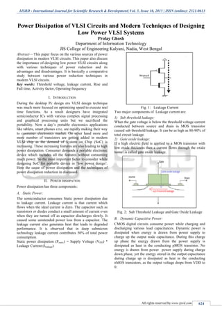
  • 1. IJSRD - International Journal for Scientific Research & Development| Vol. 3, Issue 10, 2015 | ISSN (online): 2321-0613 All rights reserved by www.ijsrd.com 624 Power Dissipation of VLSI Circuits and Modern Techniques of Designing Low Power VLSI Systems Prolay Ghosh Department of Information Technology JIS College of Engineering Kalyani, Nadia, West Bengal Abstract— This paper focus on the various sources of power dissipation in modern VLSI circuits. This paper also discuss the importance of designing low power VLSI circuits along with various techniques of power reduction and its advantages and disadvantages. It is basically a comparative study between various power reduction techniques in modern VLSI circuits. Key words: Threshold voltage, leakage current, Rise and Fall time, Activity factor, Operating frequency I. INTRODUCTION During the desktop Pc design era VLSI design technique was much more focused on optimizing speed to execute real time functions. As a result designers have integrated semiconductor ICs with various complex signal processing and graphical processing units but we sacrificed the portability. Now a day’s portable electronics applications like tablets, smart phones e.t.c. are rapidly making their way to consumer electronics market. On other hand more and more number of transistors are getting added in modern VLSI chip as the demand of System on Chip (SoC) is increasing. These increasing features are also leading to high power dissipation. Consumer demands a portable electronic device which includes all the features without consuming much power. So the most important factor to consider while designing SoC for portable device in ‘low power design’. Here the cause of power dissipation and the techniques of power dissipation reduction in discussed. II. POWER DISSIPATION Power dissipation has three components: A. Static Power: The semiconductor consumes Static power dissipation due to leakage current. Leakage current is that current which flows when the ideal current is Zero. The capacitor such as transistors or diodes conduct a small amount of current even when they are turned off as capacitor discharges slowly. It caused some unintended power loss from a capacitor. The leakage current also generates heat that leads to degraded performance. It is observed that in deep submicron technology leakage current contributes 50% of total power consumption. Static power dissipation (Pstatic) = Supply Voltage (VDD) * Leakage Current (Ileakage) Fig. 1: Leakage Current Two major components of Leakage current are: 1) Sub threshold leakage: When the gate voltage is below the threshold voltage current conducted between source and drain in MOS transistor caused sub threshold leakage. It can be as high as 80-90% of total circuit leakage. 2) Gate oxide leakage: If a high electric field is applied to a MOS transistor with low oxide thickness then a current flows through the oxide tunnel is called gate oxide leakage. Fig. 2: Sub Threshold Leakage and Gate Oxide Leakage B. Dynamic Capacitive Power: CMOS digital circuits consume power while charging and discharging various load capacitances. Dynamic power is dissipated when energy is drawn from power supply to charge up the output node capacitance. During this charge up phase the energy drawn from the power supply is dissipated as heat in the conducting pMOS transistor. No energy is drawn from power power supply during charge down phase, yet the energy stored in the output capacitance during charge up is dissipated as heat in the conducting nMOS transistors, as the output voltage drops from VDD to 0.
  • 2. Power Dissipation of VLSI Circuits and Modern Techniques of Designing Low Power VLSI Systems (IJSRD/Vol. 3/Issue 10/2015/133) All rights reserved by www.ijsrd.com 625 Fig. 3: Dynamic Capacitive Power Pdynamic = load capacitance(CL) * VDD 2 * operating frequency(Fop) The dynamic capacitive power dissipation is based on the assumption that the output node undergoes one power-consuming transition (0 to VDD) in each clock cycle. This assumption is not always correct. Depending on the circuit topology, logic style and the input signal statistics the node transition rate can be slower than the clock rate. So we introduce node transition factor or activity factor (α), which is effective number of power consuming voltage transitions experienced per clock cycle. It is directly proportional to dynamic power consumption. So the previously stated equation of dynamic capacitive power is modified as Pdynamic = α *CL* VDD 2 * Fop C. Dynamic Short-Circuit Power: Short-circuit power, is caused by the short circuit currents that arise when pairs of pMOS/nMOS transistors are conducting simultaneously. As the input voltage makes a transition from logic 0 to 1,ideally pMOS should turned off and nMOS should turned on. But the process takes small time till then both the transistors remain on and it provides a short circuit path from supply voltage to ground. Short-circuit power (Psc) = VDD * time of slope (Tsc) *Imax. Fig. 4: Dynamic Short-Circuit Power III. POWER DISSIPATION REDUCTION TECHNIQUE We have discussed various components of power dissipation. Now we have to think about the power dissipation reduction technique A. Static power consumption reduction: Static power consumption can be reduced if we can reduce the supply voltage and leakage current. 1) Supply voltage reduction: Supply voltage has direct relation with power consumption. Supply voltage of 3.3V is widely used in present days MOSFET. Experiment has shows that if we can scale down supply voltage to 1V power consumption will be reduced 10 times as shows in figure 5. Fig. 5: Supply Voltage Vs Power Consumption Supply voltage scaling is a god technique to reduce power consumption it affects the performance of the circuit as it caused drastic increase in gate delay. So in modern VLSI circuits we have to maintain a balance between speed and power. 2) Variation of threshold voltage: Threshold voltage is defined as the minimum voltage that required to make the transistor ON. Transistor maybe either nMOS or pMOS. For nMOS the threshold voltage is positive and for pMOS threshold voltage is positive. The threshold voltage ( Vth) of a field effect transistor (FET) is the value of the gate-source voltage(Vgs) when the conducting channel just begins to connect the source and drain contacts of the transistor, allowing significant current to flow. If Vgs is less than Vth then there will be no current flow. Fig. 6: Threshold Voltage a) Multiple threshold CMOS circuit (MTCMOS): The new MTCMOS circuit technology is proposed to satisfy both requirements of lowering the threshold voltage of a MOSFET and reducing stand-by current, both of which are necessary to obtain high-speed low-power performance at a supply voltage of 1V. This technology has two main features. One is that N-channel and P-channel MOSFET's
  • 3. Power Dissipation of VLSI Circuits and Modern Techniques of Designing Low Power VLSI Systems (IJSRD/Vol. 3/Issue 10/2015/133) All rights reserved by www.ijsrd.com 626 with two different threshold voltages are employed in a single chip. The other one is two operational modes, "active" and "sleep," for efficient power management. MOS transistors with low threshold voltage (Vth) are placed in the critical path while MOS transistors with high threshold voltage (Vth), are placed in the non-critical path. In the critical path gate delay time should be as low as possible. Hence delay reduction is traded off against leakage by placing low threshold transistors causing faster gate transitions. However, in the non timing critical path, high threshold transistors are placed to reduce leakage as speed/delay has less importance here. It is observed that in modern VLSI circuits as used in industry, 80% of the paths are non-timing critical. Data path can be broadly classified into two categories Timing Critical and non-Timing Critical. Here, Critical path means the path having the largest timing delay. The logic gate is composed of MOSFET's with a low threshold voltage of about 0.2-0.3 V. Its power terminals are not connected directly to the power supply lines VDD and GND, but rather to the "virtual" power supply lines VDDV and GNDV. The real and virtual power lines are linked by MOSFET's QI and Q2. These have a high threshold voltage of about 0.5-0.6 V and serve as sleep control transistors. Signals SL and SL, which are connected to the gates of QI and Q2, respectively, are used for active/sleep mode control. Circuit operation in each mode at a supply voltage of 1V is described below. Fig: 7: Example of Multiple Threshold Voltage CMOS In the active mode, when SL is set low, QI and Q2 are turned on and their on-resistance is so small that VDDV and GNDV function as real power lines. Therefore, the NAND gate operates normally and at a high speed because the Vth of 0.3 V is low enough relative to the supply voltage of 1 V. In the sleep mode, when SL is set high, Ql and Q2 are turned off so that the virtual lines VDDV and GNDV are assumed to be floating. The relatively large leakage current, determined by the subthreshold characteristics of low-Vth MOSFET's, is almost completely suppressed by Ql and Q2 since they have a high Vth and thus a much lower leakage current. Therefore, power consumption during the stand-by period can be dramatically reduced by the sleep control. It should be pointed out that two other factors affect the speed performance of an MTCMOS circuit. One is the size of the sleep control transistors Ql and Q2, and the other is the capacitances CV1 and CV2 of the virtual power lines. b) Variable threshold CMOS circuit (VTCMOS): In VTCMOS technique the threshold voltage is varied by a suitable control circuit according to the circuit requirements. As is evident from the expression above, threshold voltage is a function of the source to body bias. Hence variation of this bias voltage using suitable circuitry can vary threshold voltage. Practically for critical paths threshold voltage is lowered as switching speed is of primary concern for such paths. But for non-critical paths threshold voltage is increased to reduce the leakage power dissipation, as higher threshold prevents any sort of unwanted leakage power flow. VBN=0V are produced for PMOS and NMOS respectively. Due to this, the circuit has high switching speed (due to low Vth) at the cost of leakage power. In standby mode the control circuit generates a lower substrate voltage for NMOS and higher substrate voltage for PMOS .This causes the threshold voltage of both the NMOS and PMOS to increase, thus reducing the leakage current. Besides changing the supply voltage (VDD) and the threshold voltage (Vth). Fig. 8: Example of Variable Threshold Voltage CMOS 3) Dynamic Threshold MOS: In dynamic threshold CMOS (DTMOS), the threshold voltage is altered dynamically to suit the operating state of the circuit. A high threshold voltage in the standby mode gives low leakage current, while a low threshold voltage allows for higher current drives in the active mode of operation. Dynamic threshold CMOS can be achieved by tying the gate and body together. The supply voltage of DTMOS is limited by the diode built-in potential in bulk silicon technology. The pn diode between source and body should be reverse biased. Hence, this technique is only suitable for ultralow voltage (0.6V and below) circuits in bulk CMOS. Fig. 9: FTCMOS Circuit
  • 4. Power Dissipation of VLSI Circuits and Modern Techniques of Designing Low Power VLSI Systems (IJSRD/Vol. 3/Issue 10/2015/133) All rights reserved by www.ijsrd.com 627 4) Gate Leakage prevention: In deep sub-micron technology, gate oxide thickness reached 10-20A0 causing exponential increase in tunneling current through extremely thin gate oxide. In 45nm technology, gate leakage got increased by 10 times with respect to previous process technology. Hence, thicker insulator is used to reduce gate leakage. Thicker insulator (increase in Tox) reduces Cox, i.e the gate oxide capacitance per unit area = (K/Tox, where K= permitivitty of gate oxide) causing increase in threshold voltage (Vth) and thus reducing device speed. Hence, to keep Cox constant, different insulating materials having higher permittivity than SiO2 is used from 45nm technology onwards. Since insulating material is changed, polysilicon gate is also replaced by new metal gate to maintain low work function. B. Dynamic capacitive power consumption reduction: Dynamic power dissipation depends on four parameters namely Load Capacitance (CL), Supply Voltage (VDD), Activity factor (α) and frequency (Fop). Their impacts and way of reducing power dissipation are discussed below. 1) Load Capacitance: In modern SOC applications, large load capacitance may appear due to high fanout net or long wire distance between driver and receiver gate resulting in increase in dynamic power dissipation. a) Reduction Technique: To improve power performance down sizing driver and receiver gate is popular technique. By downsizing a transistor, the design can be more compact. Proper placement androuting is also necessary so that the length of the wire can be minimized to reduce load capacitance. Decreasing Capacitance is also difficult as it need to scale down the device and wiring. 2) Activity factor: The toggling rate of a signal with respect to clock is termed as Activity factor (α). Dynamic power dissipation is directly proportional to α. a) Reduction Technique: To reduce Activity factor, most popular technique used in industry is Clock Gating. In this method, the clock signal to different functional block is gated by enabling signals. In most cases, AND gates are preferred for gating clock signals. Fig. 10: Clock Gating The above diagram illustrates the concept of clock gating. When ENABLE=1, clock can be applied to functional block through AND gate. However to avoid unnecessary switching when the functional block is inactive, the ENABLE input can be made 0 so as to disable the clock propagation when not required. This causes the clock to become totally inactive when the functional block is in nonactive mode, thus eliminating any sort of activity in the circuit. Clock Gating can reduce power leak dueto dynamic power by as high as 70 to 80%. 3) Operating frequency: Sometime higher frequency is needed for better performance but it causes high power consumption. Introducing parallel processing lower frequency can be obtained but it increases Hardware overhead and requires extrusive change at an architecture or algorithm design. C. Dynamic Short-Circuit power consumption education: Dynamic power dissipation depends on two parameters namely Time of the slope(TSC), Supply Voltage (VDD). 1) Time of the slope(TSC): Tsc is the duration of the slope of the input signal. This component is directly depended on the Rise time and Fall time. TSC=(TR+TF)2 we can say that fast Rise time, Fall time on input signal means lower short circuit power dissipation. Fig. 11: Rise and Fall Time The Rise time and the Fall time should be small compared to the clock period. Very large Rise time and fall time have the risk of the cycles going undetected. Large Rise and Fall time mean that the signal will be hovering around mid level for too long making the system highly susceptible to noise and multiple triggering if there is not enough hysteresis. a) Reduction technique: Rise and Fall time can be reduced by reducing the gate length of the MOSFET. Strained silicon MOSFET has also less rise and fall time than bulk sislicon MOSFET. As electrons can move 70% faster allowing strained silicon transistors to switch 5% faster. - The short circuit power can also be reduced by 1) device size reduction and 2) Increasing threshold voltage Both of which is also used for leakage reduction. In addition, the input rise and fall times for a digital gate needs to be less than an upper limit which can be taken care of during gate sizing. It is important to note that short circuit power dissipation happens only during switching (Dynamic power dissipation). Hence reduction of Activity factor (α) helps both power reductions simultaneously.
  • 5. Power Dissipation of VLSI Circuits and Modern Techniques of Designing Low Power VLSI Systems (IJSRD/Vol. 3/Issue 10/2015/133) All rights reserved by www.ijsrd.com 628 IV. CONCLUSION The increasing prominence of portable systems and the need to limit power consumption in very high density ULSI chips have led to rapid and innovative developments in low power design during the recent years. Through above discussion we get a overview about various power dissipation of any type VLSI circuit and their components. In modern VLSI circuits separate power management circuits are integrated for power distribution. As power dissipation reduction has become a matter of serious concern, various power reduction techniques are being used. A lots of researches are also going on this topic. In this paper some ideas of modern power reductions have been discussed elaborately. REFERENCES [1] Fundamentals of semiconductor device ECE 515, March 5, 2003 Hernando Valencia & Farrin Hockett. [2] 1-V power supply high speed digital circuit technology with multi threshold voltage CMOS Shin’ichiro Mutoh, Takakuni Douseki,Yqsuyuki Matsuya, Takahko Aoki, Satoshi Shigematsu and Junjo Yamada,Member IEEE [3] Low power design by G.Friedman, University of Rochester [4] New design methodologies for High speed low power XOR-XNOR circuits Shiv shankar Mishra, S. Wairya, R.K.Nagaria and S.Tiwari [5] Study the amalysys of Low power and High speed CMOS Logic Circuit in 90nm Technology Fazal Noorbashar, Ashis verma,A.M.Mahajan [6] Design Techniques for Low-Voltage High-Speed Digital Bipolar Circuits Behzad Razavi, Yusuke Ota, and Robert G. Swartz,Fellow, IEEE [7] Low Power and High Speed Multi Threshold Voltage Interface Circuits Sherif A. Tawfik and Volkan Kursun, Member, IEEE [8] Low-voltage low-power CMOS full adder, D.Radhakrishnan [9] The Effect of gate length on SOI-MOSFETs operation J.Baedi, and H.Arabshahi [10]Channel length scaling and the impact of metal gate work function on the performance of double gate-metal oxide semiconductor field-effect Transistors D RECHEM, S LATRECHE and C GONTRAND [11]Gate-Length Biasing for Runtime-Leakage Control Puneet Gupta, Puneet Sharma [12]Supply and Threshold VoltageScaling for Low Power CMOS Ricardo Gonzalez, Benjamin M. Gordon, and Mark A. Horowitz. [13]POWER REDUCTION IN MODERN VLSI CIRCUITS – A REVIEW Debopam Ghosh, Jyotirmoy Guha, Arka De, Anirban Mukherjee, Electronics and Communication Engineering Heritage Institute of Technology Kolkata, India [14]Novel Ultra Low Power Multi-threshold CMOS Technology P.Sreenivasulu1, JNTU Kakinada, G.Vinatha,DECS,Marakapur Dr. K.Srinivasa Rao,T.R.R College of Engg, Dr. A.Vinaya babu,Principal of JNTU College of Eng. [15]Variable Threshold Voltage CMOS (VTCMOS) in Series Connected Circuits, Takashi Inukai, Institute of Industrial Science, University of Tokyo, Japan Toshiro Hiramoto, Tak VLSI Design and Education Center, University of Tokyo ayasu Sakurai, Center for Collaborative Research, University of Tokyo.