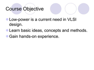
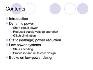
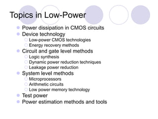
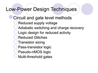
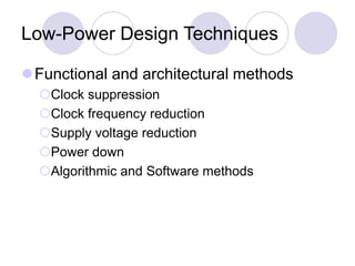
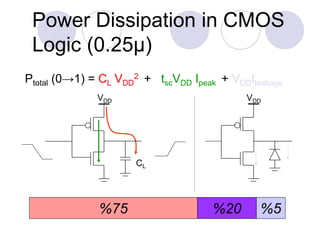
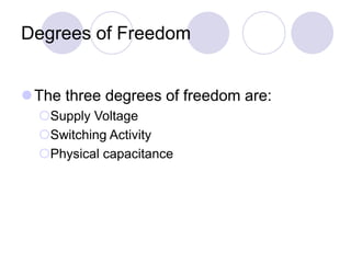
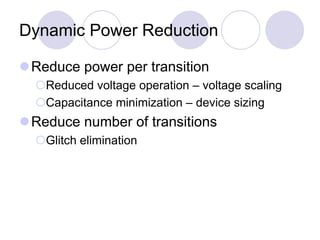
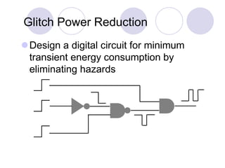
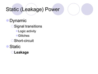
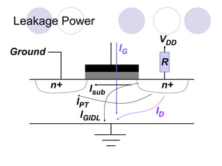
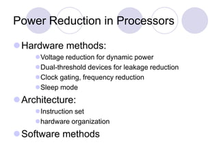
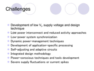
LOW POWER DESIGN
METHODS
V.ANANDI
ASST.PROF,E&C
MSRIT,BANGALORE
Course Objective
Low-power is a current need in VLSI
design.
Learn basic ideas, concepts and methods.
Gain hands-on experience.
Contents
 Introduction
 Dynamic power
Short circuit power
Reduced supply voltage operation
Glitch elimination
 Static (leakage) power reduction
 Low power systems
State encoding
Processor and multi-core design
 Books on low-power design
Introduction
Why is it a concern?
Business & technical needs
Semiconductor processing technology
Power Consumption of VLSI Chips
NEED FOR LOW POWER
More transistors are packed into the chip.
Increased market demand for portable
devices.
Environmental concerns
Meaning of Low-Power Design
 Design practices that reduce power
consumption at least by one order of magnitude;
in practice 50% reduction is often acceptable.
 General considerations in low-power design
Algorithms and architectures
High-level and software techniques
Gate and circuit-level methods
Power estimation techniques
Test power
Topics in Low-Power
 Power dissipation in CMOS circuits
 Device technology
 Low-power CMOS technologies
 Energy recovery methods
 Circuit and gate level methods
 Logic synthesis
 Dynamic power reduction techniques
 Leakage power reduction
 System level methods
 Microprocessors
 Arithmetic circuits
 Low power memory technology
 Test power
 Power estimation methods and tools
Low-Power Design Techniques
Circuit and gate level methods
Reduced supply voltage
Adiabatic switching and charge recovery
Logic design for reduced activity
Reduced Glitches
Transistor sizing
Pass-transistor logic
Pseudo-nMOS logic
Multi-threshold gates
Low-Power Design Techniques
Functional and architectural methods
Clock suppression
Clock frequency reduction
Supply voltage reduction
Power down
Algorithmic and Software methods
Power Dissipation in CMOS
Logic (0.25µ)
%75 %5
%20
Ptotal (0→1) = CL VDD
2 + tscVDD Ipeak + VDDIleakage
CL
VDD VDD
Degrees of Freedom
The three degrees of freedom are:
Supply Voltage
Switching Activity
Physical capacitance
Components of Power
Dynamic
Signal transitions
Logic activity
Glitches
Short-circuit
Static
Leakage Ptotal = Pdyn + Pstat
= Ptran + Psc + Pstat
CMOS Dynamic Power
Dynamic Power = Σ 0.5 αi fclk CLi VDD
2
All gates i
≈ 0.5 α fclk CL VDD
2
≈ α01 fclk CL VDD
2
where α average gate activity factor
α01 = 0.5α, average 0→1 trans.
fclk clock frequency
CL total load capacitance
VDD supply voltage
Dynamic Power
VDD
Ground
CL
R
R
Dynamic Power
= CLVDD
2/2 + Psc
Vi
Vo
isc
Summary: Short-Circuit Power
 Short-circuit power is consumed by each
transition (increases with input transition time).
 Reduction requires that gate output transition
should not be faster than the input transition
(faster gates can consume more short-circuit
power).
 Increasing the output load capacitance reduces
short-circuit power.
 Scaling down of supply voltage with respect to
threshold voltages reduces short-circuit power.
Dynamic Power Reduction
Reduce power per transition
Reduced voltage operation – voltage scaling
Capacitance minimization – device sizing
Reduce number of transitions
Glitch elimination
Glitch Power Reduction
Design a digital circuit for minimum
transient energy consumption by
eliminating hazards
Static (Leakage) Power
Dynamic
Signal transitions
Logic activity
Glitches
Short-circuit
Static
Leakage
Leakage Power
IG
ID
Isub
IPT
IGIDL
n+ n+
Ground
VDD
R
Leakage Current Components
Subthreshold conduction, Isub
Reverse bias pn junction conduction, ID
Gate induced drain leakage, IGIDL due to
tunneling at the gate-drain overlap
Drain source punchthrough, IPT due to
short channel and high drain-source
voltage
Gate tunneling, IG through thin oxide
Reducing Leakage Power
 Leakage power as a fraction of the total power
increases as clock frequency drops. Turning
supply off in unused parts can save power.
 For a gate it is a small fraction of the total power;
it can be significant for very large circuits.
 Scaling down features requires lowering the
threshold voltage, which increases leakage
power; roughly doubles with each shrinking.
 Multiple-threshold devices are used to reduce
leakage power.
Low-Power System Design
State encoding
Bus encoding
Finite state machine
Clock gating
Flip-flop
Shift register
Microprocessors
Single processor
Multi-core processor
Clock-Gating in Low-Power Flip-Flop
D Q
D
CK
Power Reduction in Processors
Hardware methods:
Voltage reduction for dynamic power
Dual-threshold devices for leakage reduction
Clock gating, frequency reduction
Sleep mode
Architecture:
Instruction set
hardware organization
Software methods
A Multicore Design
Multiplier
Core 1
Multiplier
Core 5
Reg
Reg
Reg
Reg
5
to
1
mux
Multiphase
Clock gen.
and mux
control
Input
Output
200MHz
CK
200MHz
40MHz
40MHz
40MHz
Multiplier
Core 2
Core clock frequency = 200/N, N should divide 200.
Challenges
 Development of low Vt, supply voltage and design
technique
 Low power interconnect and reduced activity approaches
 Low-power system synchronization
 Dynamic power-management techniques
 Development of application-specific processing
 Self-adjusting and adaptive circuits
 Integrated design methodology
 Power-conscious techniques and tools development
 Severe supply fluctuations or current spikes
REFERENCES on Low-Power Design
 A. Chandrakasan and R. Brodersen, Low-Power Digital CMOS Design,
Boston: Springer, 1995.
 A. Chandrakasan and R. Brodersen, Low-Power CMOS Design, New York:
IEEE Press, 1998.
 J. M. Rabaey and M. Pedram, Low Power Design Methodologies,
Boston: Springer, 1996.
 K. Roy and S. C. Prasad, Low-Power CMOS VLSI Circuit Design, New
York: Wiley-Interscience, 2000.
 G. K. Yeap, Practical Low Power Digital VLSI Design, Boston:Springer, 1998.
 Tutorial on low power by Vishwani.D.Aggarwal VDAT’06 Symposium on low
power design methodologies.

LPVLSI.ppt

  • 1.
  • 2.
    Course Objective Low-power isa current need in VLSI design. Learn basic ideas, concepts and methods. Gain hands-on experience.
  • 3.
    Contents  Introduction  Dynamicpower Short circuit power Reduced supply voltage operation Glitch elimination  Static (leakage) power reduction  Low power systems State encoding Processor and multi-core design  Books on low-power design
  • 4.
    Introduction Why is ita concern? Business & technical needs Semiconductor processing technology Power Consumption of VLSI Chips
  • 5.
    NEED FOR LOWPOWER More transistors are packed into the chip. Increased market demand for portable devices. Environmental concerns
  • 6.
    Meaning of Low-PowerDesign  Design practices that reduce power consumption at least by one order of magnitude; in practice 50% reduction is often acceptable.  General considerations in low-power design Algorithms and architectures High-level and software techniques Gate and circuit-level methods Power estimation techniques Test power
  • 7.
    Topics in Low-Power Power dissipation in CMOS circuits  Device technology  Low-power CMOS technologies  Energy recovery methods  Circuit and gate level methods  Logic synthesis  Dynamic power reduction techniques  Leakage power reduction  System level methods  Microprocessors  Arithmetic circuits  Low power memory technology  Test power  Power estimation methods and tools
  • 8.
    Low-Power Design Techniques Circuitand gate level methods Reduced supply voltage Adiabatic switching and charge recovery Logic design for reduced activity Reduced Glitches Transistor sizing Pass-transistor logic Pseudo-nMOS logic Multi-threshold gates
  • 9.
    Low-Power Design Techniques Functionaland architectural methods Clock suppression Clock frequency reduction Supply voltage reduction Power down Algorithmic and Software methods
  • 10.
    Power Dissipation inCMOS Logic (0.25µ) %75 %5 %20 Ptotal (0→1) = CL VDD 2 + tscVDD Ipeak + VDDIleakage CL VDD VDD
  • 11.
    Degrees of Freedom Thethree degrees of freedom are: Supply Voltage Switching Activity Physical capacitance
  • 12.
    Components of Power Dynamic Signaltransitions Logic activity Glitches Short-circuit Static Leakage Ptotal = Pdyn + Pstat = Ptran + Psc + Pstat
  • 13.
    CMOS Dynamic Power DynamicPower = Σ 0.5 αi fclk CLi VDD 2 All gates i ≈ 0.5 α fclk CL VDD 2 ≈ α01 fclk CL VDD 2 where α average gate activity factor α01 = 0.5α, average 0→1 trans. fclk clock frequency CL total load capacitance VDD supply voltage
  • 14.
  • 15.
    Summary: Short-Circuit Power Short-circuit power is consumed by each transition (increases with input transition time).  Reduction requires that gate output transition should not be faster than the input transition (faster gates can consume more short-circuit power).  Increasing the output load capacitance reduces short-circuit power.  Scaling down of supply voltage with respect to threshold voltages reduces short-circuit power.
  • 16.
    Dynamic Power Reduction Reducepower per transition Reduced voltage operation – voltage scaling Capacitance minimization – device sizing Reduce number of transitions Glitch elimination
  • 17.
    Glitch Power Reduction Designa digital circuit for minimum transient energy consumption by eliminating hazards
  • 18.
    Static (Leakage) Power Dynamic Signaltransitions Logic activity Glitches Short-circuit Static Leakage
  • 19.
  • 20.
    Leakage Current Components Subthresholdconduction, Isub Reverse bias pn junction conduction, ID Gate induced drain leakage, IGIDL due to tunneling at the gate-drain overlap Drain source punchthrough, IPT due to short channel and high drain-source voltage Gate tunneling, IG through thin oxide
  • 21.
    Reducing Leakage Power Leakage power as a fraction of the total power increases as clock frequency drops. Turning supply off in unused parts can save power.  For a gate it is a small fraction of the total power; it can be significant for very large circuits.  Scaling down features requires lowering the threshold voltage, which increases leakage power; roughly doubles with each shrinking.  Multiple-threshold devices are used to reduce leakage power.
  • 22.
    Low-Power System Design Stateencoding Bus encoding Finite state machine Clock gating Flip-flop Shift register Microprocessors Single processor Multi-core processor
  • 23.
    Clock-Gating in Low-PowerFlip-Flop D Q D CK
  • 24.
    Power Reduction inProcessors Hardware methods: Voltage reduction for dynamic power Dual-threshold devices for leakage reduction Clock gating, frequency reduction Sleep mode Architecture: Instruction set hardware organization Software methods
  • 25.
    A Multicore Design Multiplier Core1 Multiplier Core 5 Reg Reg Reg Reg 5 to 1 mux Multiphase Clock gen. and mux control Input Output 200MHz CK 200MHz 40MHz 40MHz 40MHz Multiplier Core 2 Core clock frequency = 200/N, N should divide 200.
  • 26.
    Challenges  Development oflow Vt, supply voltage and design technique  Low power interconnect and reduced activity approaches  Low-power system synchronization  Dynamic power-management techniques  Development of application-specific processing  Self-adjusting and adaptive circuits  Integrated design methodology  Power-conscious techniques and tools development  Severe supply fluctuations or current spikes
  • 27.
    REFERENCES on Low-PowerDesign  A. Chandrakasan and R. Brodersen, Low-Power Digital CMOS Design, Boston: Springer, 1995.  A. Chandrakasan and R. Brodersen, Low-Power CMOS Design, New York: IEEE Press, 1998.  J. M. Rabaey and M. Pedram, Low Power Design Methodologies, Boston: Springer, 1996.  K. Roy and S. C. Prasad, Low-Power CMOS VLSI Circuit Design, New York: Wiley-Interscience, 2000.  G. K. Yeap, Practical Low Power Digital VLSI Design, Boston:Springer, 1998.  Tutorial on low power by Vishwani.D.Aggarwal VDAT’06 Symposium on low power design methodologies.