Downloaded 777 times

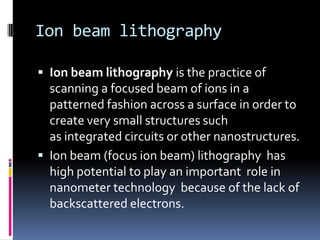
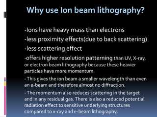
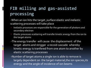
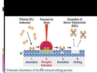
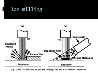
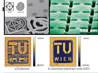
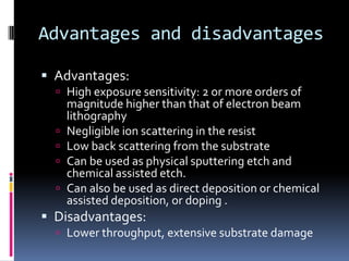
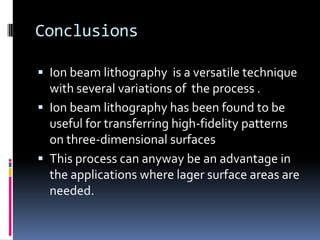


The document discusses ion-beam lithography, which uses a focused beam of ions instead of electrons or photons to pattern surfaces. Ion-beam lithography offers higher resolution than other lithography techniques due to ions having higher momentum and less scattering. It can define patterns through physical sputtering, chemical reactions with precursor gases, or ion implantation. While having advantages like high resolution and minimal proximity effects, it also has lower throughput and can damage substrates more than other lithography methods. The document provides details on ion sources, lithography processes, advantages and disadvantages of the technique.


