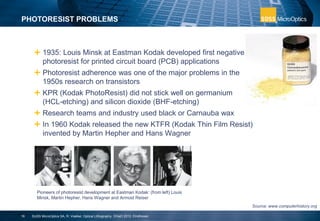
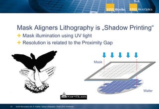
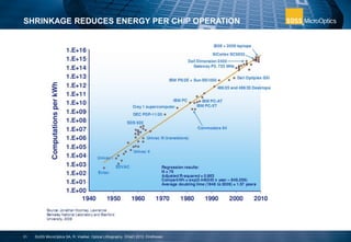
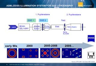
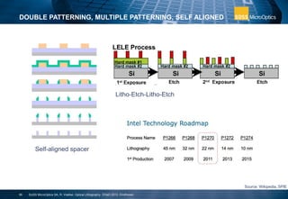
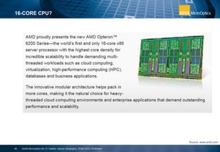
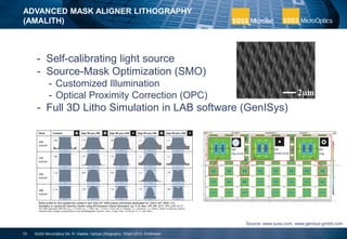
OPTICAL LITHOGRAPHY
KEY ENABLING TECHNOLOGY FOR OUR MODERN WORLD
Dr. Reinhard Voelkel
CEO SUSS MicroOptics SA
Switzerland
Invited Talk at DGaO Annual Meeting 2012, Eindhoven, The Netherlands
SUSS MicroOptics is part of the
SUSS MicroTec group,
formerly known as Karl Suss,
supplying lithography tools
(mask aligners) since 1963.
SUSS MicroOptics SA, R. Voelkel, Optical Lithography, DGaO 2012, Eindhoven2
My talk is about
îOptical Lithography -
Key Enabling Technology for our
Modern Worldî
What is our Modern World?
SUSS MicroOptics SA, R. Voelkel, Optical Lithography, DGaO 2012, Eindhoven3
OUR MODERN WORLD
Source: www.apple.com
SUSS MicroOptics SA, R. Voelkel, Optical Lithography, DGaO 2012, Eindhoven4
ONLY SOME 10 YEARS AGO
5
Source: www.wikipedia.org
SUSS MicroOptics SA, R. Voelkel, Optical Lithography, DGaO 2012, Eindhoven
6
http://www.itrs.net/Links/2011Winter/5_MEMS.pdf
SUSS MicroOptics SA, R. Voelkel, Optical Lithography, DGaO 2012, Eindhoven
LITHOGRAPHY IS KEY ENABLING TECHNOLOGY
7
Christopher J. Progler:
(CTO Photronics), at SPIE Advanced Litho, San Jose, Feb 2012
Source: www.apple.com
SUSS MicroOptics SA, R. Voelkel, Optical Lithography, DGaO 2012, Eindhoven
128GB MEMORY STICKS
8
22 nm (half-pitch) lithography
SUSS MicroOptics SA, R. Voelkel, Optical Lithography, DGaO 2012, Eindhoven
Lithography
(Greek: λίθος = lithos, 'stone' + γράφειν = graphein, 'to write')
is a method for printing using a stone
(limestone) or a metal plate with a smooth
surface.
Invented in 1796 by Bavarian author Johann
Alois Senefelder (1771 – 1834) as a cheap
method of publishing theatrical works.
Lithography can be used to print text or
artwork onto paper or other suitable material.
WIKIPEDIA
SUSS MicroOptics SA, R. Voelkel, Optical Lithography, DGaO 2012, Eindhoven9
JOHANN ALOIS SENEFELDER (1771 – 1834): LITHOGRAPHY
10
 Cheap method to publish his theatrical works?
 Paints ink as a resist on flat plates Solnhofen limestone
 Limestone is porous (hydrophilic) and absorbs ink => hydrophobic
 Gum Arabic solution absorbed at hydrophilic areas, hydrophobic
design repels
 Rolling on an ink made of soap, wax, oil and lampblack, this greasy
substance coated the design but did not spread over the moist blank
area.
 Senefelder’s invention changed printing industry: Newspapers!
Johann Alois Senefelder
(1771 – 1834)
Source: www.wikipedia.org
SUSS MicroOptics SA, R. Voelkel, Optical Lithography, DGaO 2012, Eindhoven
JOSEPH NICÉPHORE NIÉPCE (1765 – 1833): HELIOGRAPHY
11
 Photosensitive asphalt (bitumen of Judea) as photoresist
 Oiled paper with black ink as photomask
 Sun-exposure (several hours) hardens the resist
 Unexposed soft resist areas dissolved by solvents and removed Joseph Nicéphore Niépce
(1765 – 1833)
Original engraving by Isaac
Briot (1633)
Niépce’s heliography
(1826)
PortraitoftheCardinalGeorgesD’Amboise,archbishopofRouen
Source: www.wikipedia.org
SUSS MicroOptics SA, R. Voelkel, Optical Lithography, DGaO 2012, Eindhoven
Still some more inventions
needed to build my Smart
Phone...
SUSS MicroOptics SA, R. Voelkel, Optical Lithography, DGaO 2012, Eindhoven12
 John Bardeen, William Shockley and Walter Brattain
 Nobel Prize in Physics 1956
INVENTION OF THE TRANSISTOR (1947)
13
Bardeen, Shockley and Brattain
at Bell Labs (1948)
1st transistor invented at Bell Labs by
Bardeen, Shockley and Brattain in 1947
Source: www.computerhistory.org
SUSS MicroOptics SA, R. Voelkel, Optical Lithography, DGaO 2012, Eindhoven
Bell Labs
 Jules Andrus and Walter L. Bond
 Carl Frosch and Lincoln Derrick’s silicon diffusion process
DOFL: U.S. Army’s Diamond Ordnance Fuse Laboratories
 Jay W. Lathrop and James Nall: First microscope-based “stepper”
 Jay W. Lathrop and James Nall invented the name “Photolithography”
PIONEERS OF PHOTOLITHOGRAPHY IN SEMI RESEARCH
14
Jules Andrus Photoengraving
for PNPN (1957)
Lathrop/Nall: Transistor integrally mount with a printed circuit
plate by thin-film metal strips manufactured by
photolithography and vacuum deposition (1957).
SUSS MicroOptics SA, R. Voelkel, Optical Lithography, DGaO 2012, Eindhoven
Photoresist!
 1935: Louis Minsk at Eastman Kodak developed first negative
photoresist for printed circuit board (PCB) applications
 Photoresist adherence was one of the major problems in the
1950s research on transistors
 KPR (Kodak PhotoResist) did not stick well on germanium
(HCL-etching) and silicon dioxide (BHF-etching)
 Research teams and industry used black or Carnauba wax
 In 1960 Kodak released the new KTFR (Kodak Thin Film Resist)
invented by Martin Hepher and Hans Wagner
PHOTORESIST PROBLEMS
16
Pioneers of photoresist development at Eastman Kodak: (from left) Louis
Minsk, Martin Hepher, Hans Wagner and Armost Reiser
Source: www.computerhistory.org
SUSS MicroOptics SA, R. Voelkel, Optical Lithography, DGaO 2012, Eindhoven
Integrated Circuits
(IC)
 Jack S. Kilby from Texas Instruments had the “Monolithic Idea”
to integrate resistors, capacitors and transistors in a single chip.
Kilby filed his patent for an “Integrated Circuit” on Feb 6, 1959.
 At the same time Robert Noyce from Fairchild invented the
“Planar Integrated Circuit” and filed his patent on Jul 30, 1959.
 After a short patent-war they cross-licensed their patents.
INVENTION OF THE INTEGRATED CIRCUIT (1958)
18
Jack S. Kilby
(1923 – 2005)
Integrated circuit (IC) built at Texas
Instruments by Jack S. Kilby in 1958
Robert N. Noyce
(1927 - 1990)
Noyce’s integrated circuit (IC) chip as
manufactured by Fairchild in 1961
Source: www.computerhistory.org
SUSS MicroOptics SA, R. Voelkel, Optical Lithography, DGaO 2012, Eindhoven
Planar Process
 Jean Hoerni invented in 1957 the revolutionary “Planar Process”,
still the base of all semiconductor manufacturing today.
 Thin SiO2 film was photo structured and etched
 Fairchild starts production of planar transistors in 1959
THE PLANAR PROCESS (1957)
20
Jean Hoerni
(1924 - 1997)
Source: www.computerhistory.org
SUSS MicroOptics SA, R. Voelkel, Optical Lithography, DGaO 2012, Eindhoven
 1957 the eight founders left Shockley and founded
Fairchild in Palo Alto
 Fundamental inventions like the “Planar Process”
and the “Planar Integrated Circuit” allowed
industrial manufacturing of transistors and ICs
 Fairchild licensed their process to other companies
 Silicon Valley
 Semiconductor equipment manufacturers
 Requirement for lithography tools!!!
THE INCREDIBLE FAIRCHILD START-UP
21
The eight founders of Fairchild in 1960: (from left) Gordon
Moore, Sheldon Roberts, Eugene Kleiner, Robert Noyce,
Victor Grinich, Julius Blank, Jean Hoerni, and Jay Last
Noyce’s integrated circuit (IC) chip as
manufactured by Fairchild in 1961
Jean Hoerni’s planar process as
patented in 1957
Source: www.computerhistory.org
SUSS MicroOptics SA, R. Voelkel, Optical Lithography, DGaO 2012, Eindhoven
1960 – 1980
The Golden Age of
Mask Aligner
Mask Aligners Lithography is „Shadow Printing“
 Mask illumination using UV light
 Resolution is related to the Proximity Gap
23
Wafer
Mask
SUSS MicroOptics SA, R. Voelkel, Optical Lithography, DGaO 2012, Eindhoven
LITHOGRAPHY IN 1976
25
Semiconductor Feature
Sizes (Half-Pitch)
micron
1957 120
1963 30
1971 10
1974 6
1976 3
1982 1.5
1985 1.3
1989 1
SUSS MicroOptics SA, R. Voelkel, Optical Lithography, DGaO 2012, Eindhoven
Shrinkage in
Lithography
In 1959, when computers filled rooms Feynman had the vision to miniaturize
computers and chips towards their physical limits.
”Why can’t we make them (computers) very small, make them of little
wires, little elements - and by little, I mean little. For instance, the
wires should be 10 or 100 atoms in diameter, and the circuits should
be a few thousand angstroms across.”
THERE IS PLENTY OF ROOM AT THE BOTTOM
27
Source: www.wikipedia.org
SUSS MicroOptics SA, R. Voelkel, Optical Lithography, DGaO 2012, Eindhoven
JACK S. KILBY’S NOBEL PRIZE LECTURE (2000)
28
Smaller features, lower costs, larger market,
(from Jack S. Kilby’s nobel lecture in 2000)
Jack S. Kilby
(1923 – 2005)
22nm
Source: www.wikipedia.org
SUSS MicroOptics SA, R. Voelkel, Optical Lithography, DGaO 2012, Eindhoven
MOORE’S LAW
29
Source: www.wikipedia.org
SUSS MicroOptics SA, R. Voelkel, Optical Lithography, DGaO 2012, Eindhoven
SHRINKAGE REDUCES ENERGY PER CHIP OPERATION
31 SUSS MicroOptics SA, R. Voelkel, Optical Lithography, DGaO 2012, Eindhoven
THE FUTURE OF SHRINKAGE?
32 SUSS MicroOptics SA, R. Voelkel, Optical Lithography, DGaO 2012, Eindhoven
Intel’s 22nm Tri-Gate transistor is a fundamental
change:
 37% faster and 50% power reduction
Change from “Sandy Bridge” to “Ivy Bridge” in 2012
INTEL’S 3D TRANSISTORS
33
source: www.intel.com
SUSS MicroOptics SA, R. Voelkel, Optical Lithography, DGaO 2012, Eindhoven
 Optical lithography made the most important
contributions to allow the profitable continuation of
Mooreís Law.
 However, providing leading-edge lithography tools
was always a very challenging and selective
business.
 Those equipment suppliers who were not able to
provide next generation lithography (NGL) were often
kicked out of business.
 Only the winners who provided the leading-edge
lithography tools, achieved good margins and could
afford to continue their cost-intensive development
of the next generation tool.
 But even for winners it was often very difficult to
make the right choices regarding the future
technology.
MOORE’S LAW AND ITS CONSEQUENCES FOR SUPPLIERS
SUSS MicroOptics SA, R. Voelkel, Optical Lithography, DGaO 2012, Eindhoven34
LITHOGRAPHY IN 1980
Semiconductor Feature
Sizes (Half-Pitch)
micron
1957 120
1963 30
1971 10
1974 6
1976 3
1982 1.5
1985 1.3
1989 1
HISTORIC LITHO TOOL PRICE [US$]
37
Mask Aligner
Front-End Litho Tool
EUVL
ASML 1950i
Every 4 years the price doubles
[1970 – 2010]
SUSS MicroOptics SA, R. Voelkel, Optical Lithography, DGaO 2012, Eindhoven
Scanner and Stepper
SCANNER AND STEPPER
Source: Perkin-Elmer, ASML, Zeiss, Herbert Gross: Handbook of Optical Systems
X-Ray Lithography
1992: SUSS MASK ALIGNER XRS-200 (X-RAY)
Source: www.suss.com
SUSS MicroOptics SA, R. Voelkel, Optical Lithography, DGaO 2012, Eindhoven41
Customized
Illumination
CUSTOMIZED ILLUMINATION IN DUV LITHOGRAPHY
43
Source: www.zeiss.com
SUSS MicroOptics SA, R. Voelkel, Optical Lithography, DGaO 2012, Eindhoven
ASML/ZEISS ILLUMINATION SYSTEM FOR DUV LITHOGRAPHY
Source: EPFL/IMT, Carl Zeiss SMT GmbH
SUSS MicroOptics SA, R. Voelkel, Optical Lithography, DGaO 2012, Eindhoven44
FLEXRAY ILLUMINATION SYSTEM
Diffractive Optical ElementsMEMS Mirror Arrays
(FlexRay™)
Source: EPFL/IMT, ASML, Carl Zeiss SMT GmbH
SUSS MicroOptics SA, R. Voelkel, Optical Lithography, DGaO 2012, Eindhoven46
SUSS MicroOptics SA is "Preferred Supplier" for Carl Zeiss SMT GmbH
157nm Lithography?
Next:
Immersion Lithography
 Mar 2002: Burn Lin (TSMC) suggested to consider
immersion lithography @SPIE in Santa Clara.
 Oct 2003: ASML and IMEC demonstrate feasibility
 Jan 2004: Industry shifts from 157nm to immersion
 End 2004: Multiple 0.85NA immersion scanners
shipped to (TSMC, IMEC)
 2011: ASML NXT:1950i Step and Scan
 In-line catadioptric lens design (1.35NA, TWINSCAN)
 Resolution 40nm (C-quad), 38nm (dipole), 2.5 nm overlay
 FlexRay (customized illumination)
 FlexWave (programmable wavefronts)
 Reticle Control (heating compensation)
IMMERSION LITHOGRAPHY
Source:IMEC,www.dnse.com,ASML,Fabtech
SUSS MicroOptics SA, R. Voelkel, Optical Lithography, DGaO 2012, Eindhoven48
SUSS MicroOptics SA is "Preferred Supplier" for Carl Zeiss SMT GmbH
SUCCESS STORY
SUSS MicroOptics SA, R. Voelkel, Optical Lithography, DGaO 2012, Eindhoven49
SUSS MicroOptics SA is "Preferred Supplier" for Carl Zeiss SMT GmbH
THE FUTURE OF LITHOGRAPHY?
50 SUSS MicroOptics SA, R. Voelkel, Optical Lithography, DGaO 2012, Eindhoven
EUV Lithography
EUV LITHOGRAPHY
52
Source!!
Source: ASML, XTREME
SUSS MicroOptics SA, R. Voelkel, Optical Lithography, DGaO 2012, Eindhoven
Tricks & Tweaks?
Workarounds?
Moore’s Law: Double function every 2 years!
 Reduce cost per function
 Making chips more powerful for same cost, or
 Making chips of a given capability cheaper
Litho Tools: Prices doubles every 4.4 years!
RULE: Cost per function must decrease about 30%
per year - a factor of 2 every two years - to stay on
track!
THE LAWS OF SEMICONDUCTOR INDUSTRY
54
Source: Chris Mack, www.lithoguru.com
SUSS MicroOptics SA, R. Voelkel, Optical Lithography, DGaO 2012, Eindhoven
Tricks & Tweaks:
Double-Patterning
Self-Aligned ...
DOUBLE PATTERNING, MULTIPLE PATTERNING, SELF ALIGNED
Self-aligned spacer
Source: Wikipedia, SPIE
Litho-Etch-Litho-Etch
SUSS MicroOptics SA, R. Voelkel, Optical Lithography, DGaO 2012, Eindhoven56
The End of Shrinkage?
CRUSING SPEED OF COMMERCIAL AIRCRAFT
59
Source: Chris Mack, www.lithoguru.com
SUSS MicroOptics SA, R. Voelkel, Optical Lithography, DGaO 2012, Eindhoven
16-CORE CPU?
60
Source: www.amd.com
SUSS MicroOptics SA, R. Voelkel, Optical Lithography, DGaO 2012, Eindhoven
Less-Litho-Intensive-
Approach?
Yes & More Tricks:
3D Integration
3D IC, 3D Memory
3D INTEGRATION, STACKING
63
2D Integration 3D Integration
Source: www.yole.fr
SUSS MicroOptics SA, R. Voelkel, Optical Lithography, DGaO 2012, Eindhoven
MORE 3D INTEGRATION
Source: www.yole.fr
Where is the Mask
Aligner?
LITHOGRAPHY FOR LED MANUFACTURING
66
Market Share LED Exposure Tools
SUSS
Mask Aligner
ASML
Stepper
Beta Square
used Perkin Elmer
DNK
Aligner
Nikon
Used Stepper
Ultratech
Stepper
Ushio
full-field
EVG
Mask Aligner
ELS
Aligner
China 102 23 3 128
80% 18% 2%
Europe 6 1 1 8
75% 13% 13%
Japan 22 22
100%
Korea 14 9 25 1 2 51
27% 18% 49% 2% 4%
Malaysia 4 1 5
80% 20%
Singapore 20 20
100%
Taiwan 23 75 23 14 9 144
16% 52% 16% 10% 6%
USA 11 11
100%
Worldwide 182 20 2 107 48 14 1 6 9 389
Source: www.yole.fr
SUSS MicroOptics SA, R. Voelkel, Optical Lithography, DGaO 2012, Eindhoven
MASK ALIGNER 2012
ICs &
Components End Products End User
Equipment
Supplier
Research
Institutes
Source: www.suss.com
New Mask Aligner?
Mask Aligner technology changed tremendously over
the last 50 years
Mask Aligners 1963 - 2012
The optics did not for 30 years!
1969: MJB3 1985: MA150 2010: MA200 Compact
Source: www.suss.com
SUSS MicroOptics SA, R. Voelkel, Optical Lithography, DGaO 2012, Eindhoven69
NEW: MO EXPOSURE OPTICS®
SELF CALIBRATING MASK ALIGNER ILLUMINATION
Microlens Optical Integrators
 Lamp readjustment required
 Uniformity change over lamp lifetime
 Daily uniformity test required
 Variation of illumination light over mask
(angular spectrum)
NO
NO
NO
NO
Source: www.suss.com
SUSS MicroOptics SA, R. Voelkel, Optical Lithography, DGaO 2012, Eindhoven70
 Illumination technology from Stepper in Mask Aligner
 Microlens Integrators for light homogenization
 Self-calibrating light source, telecentric illumination
 Illumination filter plates allow customized illumination
 Source-Mask Optimization (SMO) in Mask Aligner
MO EXPOSURE OPTICS®
Advanced Mask Aligner Lithography (AMALITH)
Source: www.suss.com
SUSS MicroOptics SA, R. Voelkel, Optical Lithography, DGaO 2012, Eindhoven71
- Self-calibrating light source
- Source-Mask Optimization (SMO)
- Customized Illumination
- Optical Proximity Correction (OPC)
- Full 3D Litho Simulation in LAB software (GenISys)
ADVANCED MASK ALIGNER LITHOGRAPHY
(AMALITH)
Source: www.suss.com, www.genisys-gmbh.com
SUSS MicroOptics SA, R. Voelkel, Optical Lithography, DGaO 2012, Eindhoven72
ENJOY THE MODERN WORLD!
Source: www.apple.com
SUSS MicroOptics SA, R. Voelkel, Optical Lithography, DGaO 2012, Eindhoven73
SUSS.
Our Solutions
Set Standards
SUSS MicroOptics SA
Rouges-Terres 61
CH-2068 Hauterive
Switzerland
Tel +41-32-564444
Fax +41-32-5664499
info@suss.ch, www.suss.ch
74 SUSS MicroOptics SA, R. Voelkel, Optical Lithography, DGaO 2012, Eindhoven

Optical Lithography, Key Enabling Technology for our Modern World

  • 1.
    OPTICAL LITHOGRAPHY KEY ENABLINGTECHNOLOGY FOR OUR MODERN WORLD Dr. Reinhard Voelkel CEO SUSS MicroOptics SA Switzerland Invited Talk at DGaO Annual Meeting 2012, Eindhoven, The Netherlands
  • 2.
    SUSS MicroOptics ispart of the SUSS MicroTec group, formerly known as Karl Suss, supplying lithography tools (mask aligners) since 1963. SUSS MicroOptics SA, R. Voelkel, Optical Lithography, DGaO 2012, Eindhoven2
  • 3.
    My talk isabout îOptical Lithography - Key Enabling Technology for our Modern Worldî What is our Modern World? SUSS MicroOptics SA, R. Voelkel, Optical Lithography, DGaO 2012, Eindhoven3
  • 4.
    OUR MODERN WORLD Source:www.apple.com SUSS MicroOptics SA, R. Voelkel, Optical Lithography, DGaO 2012, Eindhoven4
  • 5.
    ONLY SOME 10YEARS AGO 5 Source: www.wikipedia.org SUSS MicroOptics SA, R. Voelkel, Optical Lithography, DGaO 2012, Eindhoven
  • 6.
    6 http://www.itrs.net/Links/2011Winter/5_MEMS.pdf SUSS MicroOptics SA,R. Voelkel, Optical Lithography, DGaO 2012, Eindhoven
  • 7.
    LITHOGRAPHY IS KEYENABLING TECHNOLOGY 7 Christopher J. Progler: (CTO Photronics), at SPIE Advanced Litho, San Jose, Feb 2012 Source: www.apple.com SUSS MicroOptics SA, R. Voelkel, Optical Lithography, DGaO 2012, Eindhoven
  • 8.
    128GB MEMORY STICKS 8 22nm (half-pitch) lithography SUSS MicroOptics SA, R. Voelkel, Optical Lithography, DGaO 2012, Eindhoven
  • 9.
    Lithography (Greek: λίθος =lithos, 'stone' + γράφειν = graphein, 'to write') is a method for printing using a stone (limestone) or a metal plate with a smooth surface. Invented in 1796 by Bavarian author Johann Alois Senefelder (1771 – 1834) as a cheap method of publishing theatrical works. Lithography can be used to print text or artwork onto paper or other suitable material. WIKIPEDIA SUSS MicroOptics SA, R. Voelkel, Optical Lithography, DGaO 2012, Eindhoven9
  • 10.
    JOHANN ALOIS SENEFELDER(1771 – 1834): LITHOGRAPHY 10  Cheap method to publish his theatrical works?  Paints ink as a resist on flat plates Solnhofen limestone  Limestone is porous (hydrophilic) and absorbs ink => hydrophobic  Gum Arabic solution absorbed at hydrophilic areas, hydrophobic design repels  Rolling on an ink made of soap, wax, oil and lampblack, this greasy substance coated the design but did not spread over the moist blank area.  Senefelder’s invention changed printing industry: Newspapers! Johann Alois Senefelder (1771 – 1834) Source: www.wikipedia.org SUSS MicroOptics SA, R. Voelkel, Optical Lithography, DGaO 2012, Eindhoven
  • 11.
    JOSEPH NICÉPHORE NIÉPCE(1765 – 1833): HELIOGRAPHY 11  Photosensitive asphalt (bitumen of Judea) as photoresist  Oiled paper with black ink as photomask  Sun-exposure (several hours) hardens the resist  Unexposed soft resist areas dissolved by solvents and removed Joseph Nicéphore Niépce (1765 – 1833) Original engraving by Isaac Briot (1633) Niépce’s heliography (1826) PortraitoftheCardinalGeorgesD’Amboise,archbishopofRouen Source: www.wikipedia.org SUSS MicroOptics SA, R. Voelkel, Optical Lithography, DGaO 2012, Eindhoven
  • 12.
    Still some moreinventions needed to build my Smart Phone... SUSS MicroOptics SA, R. Voelkel, Optical Lithography, DGaO 2012, Eindhoven12
  • 13.
     John Bardeen,William Shockley and Walter Brattain  Nobel Prize in Physics 1956 INVENTION OF THE TRANSISTOR (1947) 13 Bardeen, Shockley and Brattain at Bell Labs (1948) 1st transistor invented at Bell Labs by Bardeen, Shockley and Brattain in 1947 Source: www.computerhistory.org SUSS MicroOptics SA, R. Voelkel, Optical Lithography, DGaO 2012, Eindhoven
  • 14.
    Bell Labs  JulesAndrus and Walter L. Bond  Carl Frosch and Lincoln Derrick’s silicon diffusion process DOFL: U.S. Army’s Diamond Ordnance Fuse Laboratories  Jay W. Lathrop and James Nall: First microscope-based “stepper”  Jay W. Lathrop and James Nall invented the name “Photolithography” PIONEERS OF PHOTOLITHOGRAPHY IN SEMI RESEARCH 14 Jules Andrus Photoengraving for PNPN (1957) Lathrop/Nall: Transistor integrally mount with a printed circuit plate by thin-film metal strips manufactured by photolithography and vacuum deposition (1957). SUSS MicroOptics SA, R. Voelkel, Optical Lithography, DGaO 2012, Eindhoven
  • 15.
  • 16.
     1935: LouisMinsk at Eastman Kodak developed first negative photoresist for printed circuit board (PCB) applications  Photoresist adherence was one of the major problems in the 1950s research on transistors  KPR (Kodak PhotoResist) did not stick well on germanium (HCL-etching) and silicon dioxide (BHF-etching)  Research teams and industry used black or Carnauba wax  In 1960 Kodak released the new KTFR (Kodak Thin Film Resist) invented by Martin Hepher and Hans Wagner PHOTORESIST PROBLEMS 16 Pioneers of photoresist development at Eastman Kodak: (from left) Louis Minsk, Martin Hepher, Hans Wagner and Armost Reiser Source: www.computerhistory.org SUSS MicroOptics SA, R. Voelkel, Optical Lithography, DGaO 2012, Eindhoven
  • 17.
  • 18.
     Jack S.Kilby from Texas Instruments had the “Monolithic Idea” to integrate resistors, capacitors and transistors in a single chip. Kilby filed his patent for an “Integrated Circuit” on Feb 6, 1959.  At the same time Robert Noyce from Fairchild invented the “Planar Integrated Circuit” and filed his patent on Jul 30, 1959.  After a short patent-war they cross-licensed their patents. INVENTION OF THE INTEGRATED CIRCUIT (1958) 18 Jack S. Kilby (1923 – 2005) Integrated circuit (IC) built at Texas Instruments by Jack S. Kilby in 1958 Robert N. Noyce (1927 - 1990) Noyce’s integrated circuit (IC) chip as manufactured by Fairchild in 1961 Source: www.computerhistory.org SUSS MicroOptics SA, R. Voelkel, Optical Lithography, DGaO 2012, Eindhoven
  • 19.
  • 20.
     Jean Hoerniinvented in 1957 the revolutionary “Planar Process”, still the base of all semiconductor manufacturing today.  Thin SiO2 film was photo structured and etched  Fairchild starts production of planar transistors in 1959 THE PLANAR PROCESS (1957) 20 Jean Hoerni (1924 - 1997) Source: www.computerhistory.org SUSS MicroOptics SA, R. Voelkel, Optical Lithography, DGaO 2012, Eindhoven
  • 21.
     1957 theeight founders left Shockley and founded Fairchild in Palo Alto  Fundamental inventions like the “Planar Process” and the “Planar Integrated Circuit” allowed industrial manufacturing of transistors and ICs  Fairchild licensed their process to other companies  Silicon Valley  Semiconductor equipment manufacturers  Requirement for lithography tools!!! THE INCREDIBLE FAIRCHILD START-UP 21 The eight founders of Fairchild in 1960: (from left) Gordon Moore, Sheldon Roberts, Eugene Kleiner, Robert Noyce, Victor Grinich, Julius Blank, Jean Hoerni, and Jay Last Noyce’s integrated circuit (IC) chip as manufactured by Fairchild in 1961 Jean Hoerni’s planar process as patented in 1957 Source: www.computerhistory.org SUSS MicroOptics SA, R. Voelkel, Optical Lithography, DGaO 2012, Eindhoven
  • 22.
    1960 – 1980 TheGolden Age of Mask Aligner
  • 23.
    Mask Aligners Lithographyis „Shadow Printing“  Mask illumination using UV light  Resolution is related to the Proximity Gap 23 Wafer Mask SUSS MicroOptics SA, R. Voelkel, Optical Lithography, DGaO 2012, Eindhoven
  • 24.
    LITHOGRAPHY IN 1976 25 SemiconductorFeature Sizes (Half-Pitch) micron 1957 120 1963 30 1971 10 1974 6 1976 3 1982 1.5 1985 1.3 1989 1 SUSS MicroOptics SA, R. Voelkel, Optical Lithography, DGaO 2012, Eindhoven
  • 25.
  • 26.
    In 1959, whencomputers filled rooms Feynman had the vision to miniaturize computers and chips towards their physical limits. ”Why can’t we make them (computers) very small, make them of little wires, little elements - and by little, I mean little. For instance, the wires should be 10 or 100 atoms in diameter, and the circuits should be a few thousand angstroms across.” THERE IS PLENTY OF ROOM AT THE BOTTOM 27 Source: www.wikipedia.org SUSS MicroOptics SA, R. Voelkel, Optical Lithography, DGaO 2012, Eindhoven
  • 27.
    JACK S. KILBY’SNOBEL PRIZE LECTURE (2000) 28 Smaller features, lower costs, larger market, (from Jack S. Kilby’s nobel lecture in 2000) Jack S. Kilby (1923 – 2005) 22nm Source: www.wikipedia.org SUSS MicroOptics SA, R. Voelkel, Optical Lithography, DGaO 2012, Eindhoven
  • 28.
    MOORE’S LAW 29 Source: www.wikipedia.org SUSSMicroOptics SA, R. Voelkel, Optical Lithography, DGaO 2012, Eindhoven
  • 29.
    SHRINKAGE REDUCES ENERGYPER CHIP OPERATION 31 SUSS MicroOptics SA, R. Voelkel, Optical Lithography, DGaO 2012, Eindhoven
  • 30.
    THE FUTURE OFSHRINKAGE? 32 SUSS MicroOptics SA, R. Voelkel, Optical Lithography, DGaO 2012, Eindhoven
  • 31.
    Intel’s 22nm Tri-Gatetransistor is a fundamental change:  37% faster and 50% power reduction Change from “Sandy Bridge” to “Ivy Bridge” in 2012 INTEL’S 3D TRANSISTORS 33 source: www.intel.com SUSS MicroOptics SA, R. Voelkel, Optical Lithography, DGaO 2012, Eindhoven
  • 32.
     Optical lithographymade the most important contributions to allow the profitable continuation of Mooreís Law.  However, providing leading-edge lithography tools was always a very challenging and selective business.  Those equipment suppliers who were not able to provide next generation lithography (NGL) were often kicked out of business.  Only the winners who provided the leading-edge lithography tools, achieved good margins and could afford to continue their cost-intensive development of the next generation tool.  But even for winners it was often very difficult to make the right choices regarding the future technology. MOORE’S LAW AND ITS CONSEQUENCES FOR SUPPLIERS SUSS MicroOptics SA, R. Voelkel, Optical Lithography, DGaO 2012, Eindhoven34
  • 33.
    LITHOGRAPHY IN 1980 SemiconductorFeature Sizes (Half-Pitch) micron 1957 120 1963 30 1971 10 1974 6 1976 3 1982 1.5 1985 1.3 1989 1
  • 35.
    HISTORIC LITHO TOOLPRICE [US$] 37 Mask Aligner Front-End Litho Tool EUVL ASML 1950i Every 4 years the price doubles [1970 – 2010] SUSS MicroOptics SA, R. Voelkel, Optical Lithography, DGaO 2012, Eindhoven
  • 36.
  • 37.
    SCANNER AND STEPPER Source:Perkin-Elmer, ASML, Zeiss, Herbert Gross: Handbook of Optical Systems
  • 38.
  • 39.
    1992: SUSS MASKALIGNER XRS-200 (X-RAY) Source: www.suss.com SUSS MicroOptics SA, R. Voelkel, Optical Lithography, DGaO 2012, Eindhoven41
  • 40.
  • 41.
    CUSTOMIZED ILLUMINATION INDUV LITHOGRAPHY 43 Source: www.zeiss.com SUSS MicroOptics SA, R. Voelkel, Optical Lithography, DGaO 2012, Eindhoven
  • 42.
    ASML/ZEISS ILLUMINATION SYSTEMFOR DUV LITHOGRAPHY Source: EPFL/IMT, Carl Zeiss SMT GmbH SUSS MicroOptics SA, R. Voelkel, Optical Lithography, DGaO 2012, Eindhoven44
  • 43.
    FLEXRAY ILLUMINATION SYSTEM DiffractiveOptical ElementsMEMS Mirror Arrays (FlexRay™) Source: EPFL/IMT, ASML, Carl Zeiss SMT GmbH SUSS MicroOptics SA, R. Voelkel, Optical Lithography, DGaO 2012, Eindhoven46 SUSS MicroOptics SA is "Preferred Supplier" for Carl Zeiss SMT GmbH
  • 44.
  • 45.
     Mar 2002:Burn Lin (TSMC) suggested to consider immersion lithography @SPIE in Santa Clara.  Oct 2003: ASML and IMEC demonstrate feasibility  Jan 2004: Industry shifts from 157nm to immersion  End 2004: Multiple 0.85NA immersion scanners shipped to (TSMC, IMEC)  2011: ASML NXT:1950i Step and Scan  In-line catadioptric lens design (1.35NA, TWINSCAN)  Resolution 40nm (C-quad), 38nm (dipole), 2.5 nm overlay  FlexRay (customized illumination)  FlexWave (programmable wavefronts)  Reticle Control (heating compensation) IMMERSION LITHOGRAPHY Source:IMEC,www.dnse.com,ASML,Fabtech SUSS MicroOptics SA, R. Voelkel, Optical Lithography, DGaO 2012, Eindhoven48 SUSS MicroOptics SA is "Preferred Supplier" for Carl Zeiss SMT GmbH
  • 46.
    SUCCESS STORY SUSS MicroOpticsSA, R. Voelkel, Optical Lithography, DGaO 2012, Eindhoven49 SUSS MicroOptics SA is "Preferred Supplier" for Carl Zeiss SMT GmbH
  • 47.
    THE FUTURE OFLITHOGRAPHY? 50 SUSS MicroOptics SA, R. Voelkel, Optical Lithography, DGaO 2012, Eindhoven
  • 48.
  • 49.
    EUV LITHOGRAPHY 52 Source!! Source: ASML,XTREME SUSS MicroOptics SA, R. Voelkel, Optical Lithography, DGaO 2012, Eindhoven
  • 50.
  • 51.
    Moore’s Law: Doublefunction every 2 years!  Reduce cost per function  Making chips more powerful for same cost, or  Making chips of a given capability cheaper Litho Tools: Prices doubles every 4.4 years! RULE: Cost per function must decrease about 30% per year - a factor of 2 every two years - to stay on track! THE LAWS OF SEMICONDUCTOR INDUSTRY 54 Source: Chris Mack, www.lithoguru.com SUSS MicroOptics SA, R. Voelkel, Optical Lithography, DGaO 2012, Eindhoven
  • 52.
  • 53.
    DOUBLE PATTERNING, MULTIPLEPATTERNING, SELF ALIGNED Self-aligned spacer Source: Wikipedia, SPIE Litho-Etch-Litho-Etch SUSS MicroOptics SA, R. Voelkel, Optical Lithography, DGaO 2012, Eindhoven56
  • 54.
    The End ofShrinkage?
  • 55.
    CRUSING SPEED OFCOMMERCIAL AIRCRAFT 59 Source: Chris Mack, www.lithoguru.com SUSS MicroOptics SA, R. Voelkel, Optical Lithography, DGaO 2012, Eindhoven
  • 56.
    16-CORE CPU? 60 Source: www.amd.com SUSSMicroOptics SA, R. Voelkel, Optical Lithography, DGaO 2012, Eindhoven
  • 57.
  • 58.
    Yes & MoreTricks: 3D Integration 3D IC, 3D Memory
  • 59.
    3D INTEGRATION, STACKING 63 2DIntegration 3D Integration Source: www.yole.fr SUSS MicroOptics SA, R. Voelkel, Optical Lithography, DGaO 2012, Eindhoven
  • 60.
  • 61.
    Where is theMask Aligner?
  • 62.
    LITHOGRAPHY FOR LEDMANUFACTURING 66 Market Share LED Exposure Tools SUSS Mask Aligner ASML Stepper Beta Square used Perkin Elmer DNK Aligner Nikon Used Stepper Ultratech Stepper Ushio full-field EVG Mask Aligner ELS Aligner China 102 23 3 128 80% 18% 2% Europe 6 1 1 8 75% 13% 13% Japan 22 22 100% Korea 14 9 25 1 2 51 27% 18% 49% 2% 4% Malaysia 4 1 5 80% 20% Singapore 20 20 100% Taiwan 23 75 23 14 9 144 16% 52% 16% 10% 6% USA 11 11 100% Worldwide 182 20 2 107 48 14 1 6 9 389 Source: www.yole.fr SUSS MicroOptics SA, R. Voelkel, Optical Lithography, DGaO 2012, Eindhoven
  • 63.
    MASK ALIGNER 2012 ICs& Components End Products End User Equipment Supplier Research Institutes Source: www.suss.com
  • 64.
  • 65.
    Mask Aligner technologychanged tremendously over the last 50 years Mask Aligners 1963 - 2012 The optics did not for 30 years! 1969: MJB3 1985: MA150 2010: MA200 Compact Source: www.suss.com SUSS MicroOptics SA, R. Voelkel, Optical Lithography, DGaO 2012, Eindhoven69
  • 66.
    NEW: MO EXPOSUREOPTICS® SELF CALIBRATING MASK ALIGNER ILLUMINATION Microlens Optical Integrators  Lamp readjustment required  Uniformity change over lamp lifetime  Daily uniformity test required  Variation of illumination light over mask (angular spectrum) NO NO NO NO Source: www.suss.com SUSS MicroOptics SA, R. Voelkel, Optical Lithography, DGaO 2012, Eindhoven70
  • 67.
     Illumination technologyfrom Stepper in Mask Aligner  Microlens Integrators for light homogenization  Self-calibrating light source, telecentric illumination  Illumination filter plates allow customized illumination  Source-Mask Optimization (SMO) in Mask Aligner MO EXPOSURE OPTICS® Advanced Mask Aligner Lithography (AMALITH) Source: www.suss.com SUSS MicroOptics SA, R. Voelkel, Optical Lithography, DGaO 2012, Eindhoven71
  • 68.
    - Self-calibrating lightsource - Source-Mask Optimization (SMO) - Customized Illumination - Optical Proximity Correction (OPC) - Full 3D Litho Simulation in LAB software (GenISys) ADVANCED MASK ALIGNER LITHOGRAPHY (AMALITH) Source: www.suss.com, www.genisys-gmbh.com SUSS MicroOptics SA, R. Voelkel, Optical Lithography, DGaO 2012, Eindhoven72
  • 69.
    ENJOY THE MODERNWORLD! Source: www.apple.com SUSS MicroOptics SA, R. Voelkel, Optical Lithography, DGaO 2012, Eindhoven73
  • 70.
    SUSS. Our Solutions Set Standards SUSSMicroOptics SA Rouges-Terres 61 CH-2068 Hauterive Switzerland Tel +41-32-564444 Fax +41-32-5664499 info@suss.ch, www.suss.ch 74 SUSS MicroOptics SA, R. Voelkel, Optical Lithography, DGaO 2012, Eindhoven