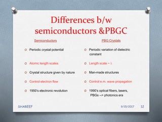
PHOTONIC
CRYSTALS
9/15/2017SHAREEF 1
CONTENTS
O CRYSTAL
O SEMICONDUCTOR
O PHOTONIC CRYSTAL
O PHOTONIC BAND GAP
O TYPES
O APPLICATIONS
9/15/2017SHAREEF 2
What is a crystal?
O A homogeneous solid formed by repeating,
Three dimensional pattern of atoms, ions, or
molecules.
O These have fixed distances between
constituent parts. (from Greek krustallos).
PHOTON:
The quantum of electromagnetic
energy, having zero mass, no electric charge,
and long lifetime.
9/15/2017SHAREEF 3
What is a semiconductor?
O It is a type of crystal whose
conductivity is in between a conductor
and insulator.
Examples: Silicon Germanium
9/15/2017SHAREEF 4
What is a photonic crystal?
O A photonic crystal is a periodic
structure in an optical medium, which
structure creates unusual optical
dispersion properties
OR
O Crystals having photonic band gap are
called photonic crystals or photonic
band gap crystals.
9/15/2017SHAREEF 5
Examples
O Examples in nature which reflect
electromagnetic radiation as
propagation through them is
prohibited.
9/15/2017SHAREEF 6
Natural opals
9/15/2017SHAREEF 7
Artificial Opal
Artificial opal sample (SEM Image)
Several cleaved planes of fcc structure are shown9/15/2017SHAREEF 8
What is Photonic Band Gap?
O Photonic band gap a range of forbidden
frequencies within which a specific
wavelength is blocked, and light is reflected
rather than transmitted.
9/15/2017SHAREEF 9
Basics of photonic band gaps
O The behavior of light in a photonic
crystal is similar to the movement
of electrons and holes in a
semiconductor.
O If the periodicity of the lattice is
broken by a missing Si atom or
by various impurity an electron
can have enough energy to be
in the band gap.
O The same for photons in a
photonic lattice, photons move
in a transparent dielectric
material that contains tiny air
holes arranged in a lattice
pattern.
9/15/2017SHAREEF 10
Bragg Reflection
2 ( )B Bnd Sin  
9/15/2017SHAREEF 11
Differences b/w
semiconductors &PBGC
Semiconductors
O Periodic crystal potential
O Atomic length scales
O Crystal structure given by nature
O Control electron flow
O 1950’s electronic revolution
PBG Crystals
O Periodic variation of dielectric
constant
O Length scale ~ 
O Man-made structures
O Control e.m. wave propagation
O 1990’s optical fibers, lasers,
PBGs --> photonics era
9/15/2017SHAREEF 12
What are different types of
PBGS?
O Periodic structure in an optical medium,
can be periodic in
O Single dimension
O Two dimensions
O Three dimensions.
9/15/2017SHAREEF 13
One Dimensional PBGC
O The material is periodic in the z-
direction, and homogeneous in the x y-
plane.
O Light propagate only in the z-direction
through 3 different 1d lattice samples.
9/15/2017SHAREEF 14
Two Dimensional PBGC
O The material has periodicity in 2
dimensions (that's where the photonic
gaps appear) and is homogeneous in
the third dimension.
O It periodic in the x y-plane and not in
the z-direction as for the 1d lattice.
9/15/2017SHAREEF 15
Three Dimensional PBGC
O A three-dimensional photonic crystal was
created using layer-by-layer periodic
structure method.
O The orientations of the axes are rotated by
90o between adjacent layers.
9/15/2017SHAREEF 16
Applications
O Suppression of spontaneous emission
9/15/2017SHAREEF 17
Applications(contd.)
O Low-threshold lasers, single-mode
LEDs, mirrors, optical filters
O Lasers and optical devices - improved
performance in efficiency and
reduction of background noise
O Fast electronics – inter chip
communication
O Medical and biological application
e.g., microwave resonance therapy (40-
80 GHz), imaging
9/15/2017SHAREEF 18
In fiber optic communication
9/15/2017SHAREEF 19
Conclusion
O Photonic crystals are going to be the
future semiconductors
O It has many applications irrespective of
fields
9/15/2017SHAREEF 20
9/15/2017SHAREEF 21

PHOTONIC CRYSTALS

  • 1.
  • 2.
    CONTENTS O CRYSTAL O SEMICONDUCTOR OPHOTONIC CRYSTAL O PHOTONIC BAND GAP O TYPES O APPLICATIONS 9/15/2017SHAREEF 2
  • 3.
    What is acrystal? O A homogeneous solid formed by repeating, Three dimensional pattern of atoms, ions, or molecules. O These have fixed distances between constituent parts. (from Greek krustallos). PHOTON: The quantum of electromagnetic energy, having zero mass, no electric charge, and long lifetime. 9/15/2017SHAREEF 3
  • 4.
    What is asemiconductor? O It is a type of crystal whose conductivity is in between a conductor and insulator. Examples: Silicon Germanium 9/15/2017SHAREEF 4
  • 5.
    What is aphotonic crystal? O A photonic crystal is a periodic structure in an optical medium, which structure creates unusual optical dispersion properties OR O Crystals having photonic band gap are called photonic crystals or photonic band gap crystals. 9/15/2017SHAREEF 5
  • 6.
    Examples O Examples innature which reflect electromagnetic radiation as propagation through them is prohibited. 9/15/2017SHAREEF 6
  • 7.
  • 8.
    Artificial Opal Artificial opalsample (SEM Image) Several cleaved planes of fcc structure are shown9/15/2017SHAREEF 8
  • 9.
    What is PhotonicBand Gap? O Photonic band gap a range of forbidden frequencies within which a specific wavelength is blocked, and light is reflected rather than transmitted. 9/15/2017SHAREEF 9
  • 10.
    Basics of photonicband gaps O The behavior of light in a photonic crystal is similar to the movement of electrons and holes in a semiconductor. O If the periodicity of the lattice is broken by a missing Si atom or by various impurity an electron can have enough energy to be in the band gap. O The same for photons in a photonic lattice, photons move in a transparent dielectric material that contains tiny air holes arranged in a lattice pattern. 9/15/2017SHAREEF 10
  • 11.
    Bragg Reflection 2 ()B Bnd Sin   9/15/2017SHAREEF 11
  • 12.
    Differences b/w semiconductors &PBGC Semiconductors OPeriodic crystal potential O Atomic length scales O Crystal structure given by nature O Control electron flow O 1950’s electronic revolution PBG Crystals O Periodic variation of dielectric constant O Length scale ~  O Man-made structures O Control e.m. wave propagation O 1990’s optical fibers, lasers, PBGs --> photonics era 9/15/2017SHAREEF 12
  • 13.
    What are differenttypes of PBGS? O Periodic structure in an optical medium, can be periodic in O Single dimension O Two dimensions O Three dimensions. 9/15/2017SHAREEF 13
  • 14.
    One Dimensional PBGC OThe material is periodic in the z- direction, and homogeneous in the x y- plane. O Light propagate only in the z-direction through 3 different 1d lattice samples. 9/15/2017SHAREEF 14
  • 15.
    Two Dimensional PBGC OThe material has periodicity in 2 dimensions (that's where the photonic gaps appear) and is homogeneous in the third dimension. O It periodic in the x y-plane and not in the z-direction as for the 1d lattice. 9/15/2017SHAREEF 15
  • 16.
    Three Dimensional PBGC OA three-dimensional photonic crystal was created using layer-by-layer periodic structure method. O The orientations of the axes are rotated by 90o between adjacent layers. 9/15/2017SHAREEF 16
  • 17.
    Applications O Suppression ofspontaneous emission 9/15/2017SHAREEF 17
  • 18.
    Applications(contd.) O Low-threshold lasers,single-mode LEDs, mirrors, optical filters O Lasers and optical devices - improved performance in efficiency and reduction of background noise O Fast electronics – inter chip communication O Medical and biological application e.g., microwave resonance therapy (40- 80 GHz), imaging 9/15/2017SHAREEF 18
  • 19.
    In fiber opticcommunication 9/15/2017SHAREEF 19
  • 20.
    Conclusion O Photonic crystalsare going to be the future semiconductors O It has many applications irrespective of fields 9/15/2017SHAREEF 20
  • 21.

Editor's Notes

  • #7 Photonic Crystals are periodic structures, there are natural examples already existing in nature which reflect electromagnetic radiation as propagation through them is prohibited.