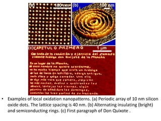
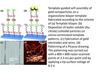
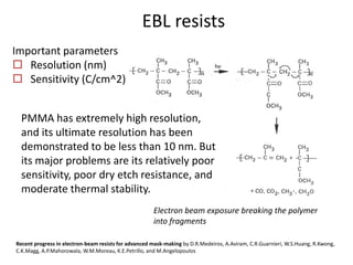
The document discusses electron beam lithography (EBL) for nano fabrication. EBL uses an electron beam to directly write nanoscale patterns on a resist-coated substrate. It allows for very high resolution down to 5 nm but has low throughput as it is a serial writing process. The key components of an EBL system include an electron gun, electron column for beam shaping and focusing, mechanical stage, wafer handling system, and control computer. EBL resists like PMMA can achieve high resolution but have limitations in sensitivity, etch resistance and thermal stability. EBL is widely used for research applications and mask making due to its high resolution, though it is too slow for high-volume manufacturing.


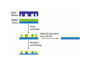
![Nanoimprint lithography (NIL)
• Nanoimprint lithography (NIL) has primarily been used to emboss
hard thermoplastic polymers. The micromolding and embossing of
elastomers has attracted considerable interest as these materials
have found important applications in softlithographic techniques
such as microcontact printing (µCP).
• In this technique, a monolayer of a material is printed off an
elastomeric stamp [made of poly(dimethylsiloxane) (PDMS)] after
forming conformal contact between stamp and substrate. Sub-
micron surface relief structures can easily be introduced in PDMS by
curing the polymers against a lithographically prepared master.
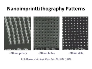
• Feature sizes in the 10–100 nm size range.
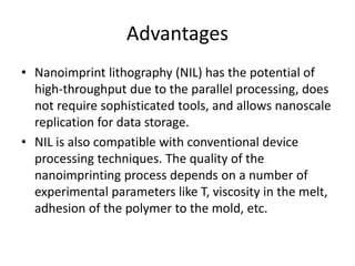
• After imprinting the polymer film, further etching can transfer the
pattern into the underlying substrate. Alternatively, metal
evaporation and lift-off of the polymer mask produces nanopattern
metal features.](https://image.slidesharecdn.com/ete444lec6nanofabricationpdf759/85/ETE444-lec6-nanofabrication-pdf-20-320.jpg)