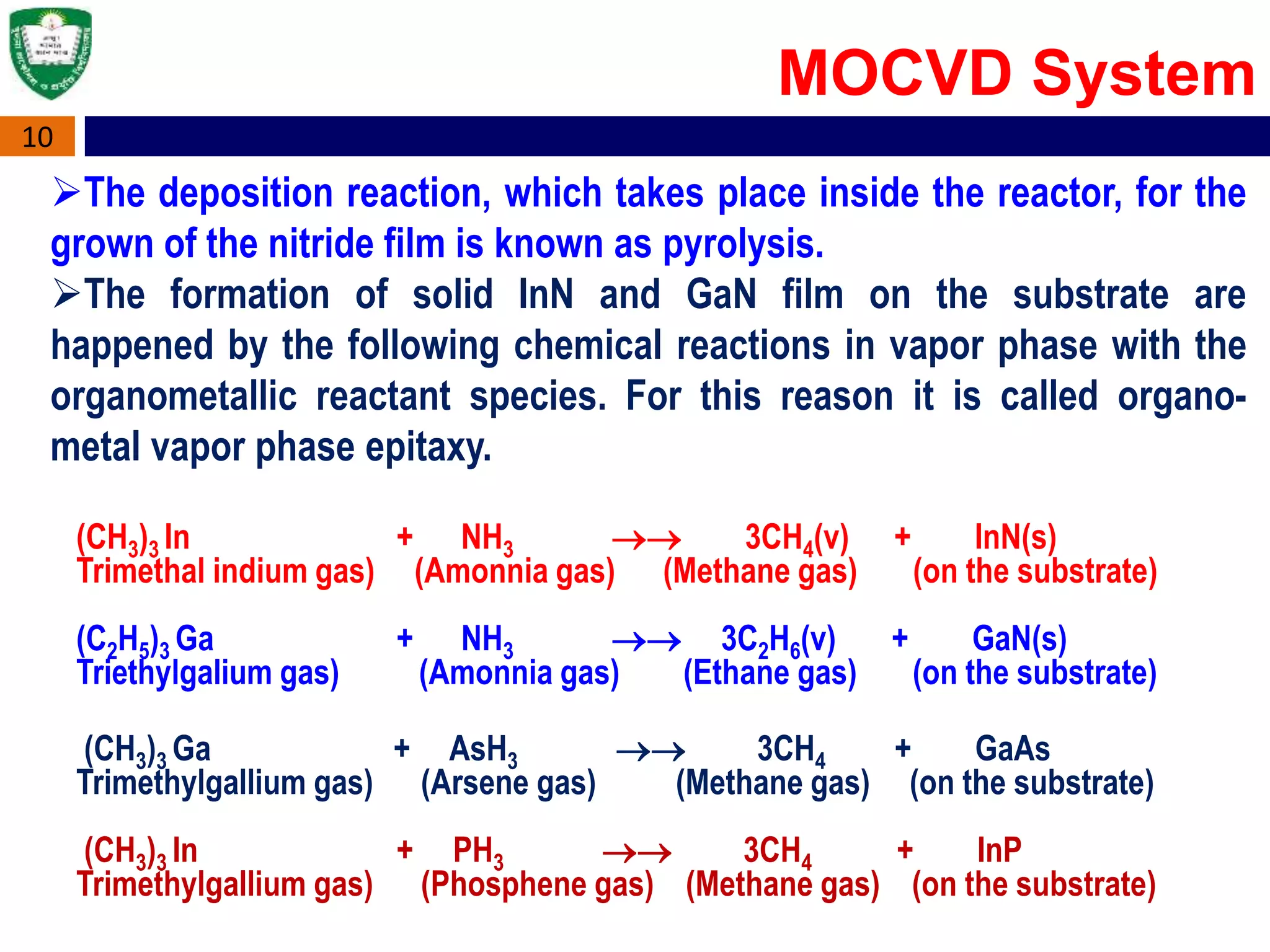
Metal Organic Chemical Vapour Deposition (MOCVD) is a technique used to grow thin semiconductor films on substrates using organometallic compounds as sources. MOCVD is commonly used to fabricate electronic and optoelectronic devices like those in phones, LEDs, and solar cells. The MOCVD process involves heating substrates in a reactor where organometallic source gases decompose and react to form epitaxial semiconductor films precisely controlled in thickness and composition. MOCVD offers high growth quality, flexibility, and throughput making it well-suited for heterostructures like quantum wells used across many applications.


![Thin_Film_Technology_introduction[1]](https://cdn.slidesharecdn.com/ss_thumbnails/1b4496c8-2102-411b-8465-a3dd3f398327-150205034538-conversion-gate02-thumbnail.jpg?width=640&height=640&fit=bounds)


