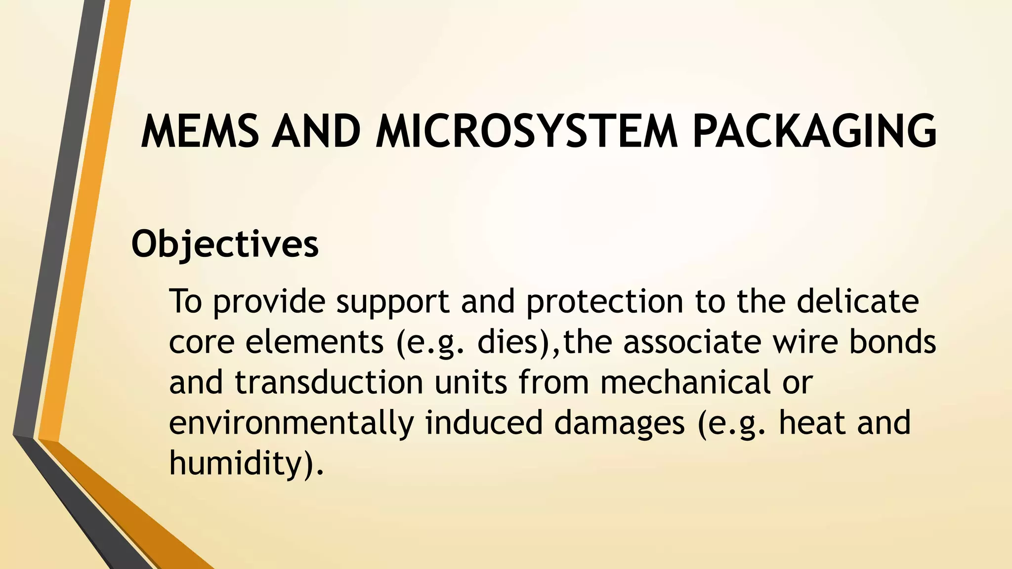
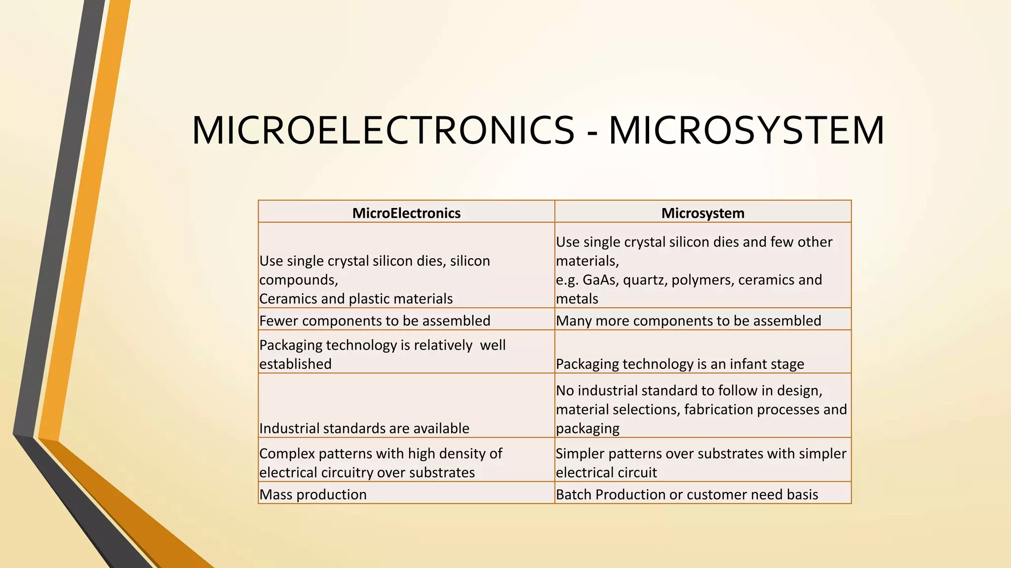
MEMS PACKAGING
Prasanna DAE.,BE(Auto).,ME
Madurai Tamilnadu
INDIA
Content
1.Mechanical packaging – Microelectronics
2.Levels of Microelectronic Packaging
3.Plastic Encapsulated of Microcircuit
4.Packaging Issues
5.MEMS and Microsystem Packaging
6.Packaging Design Consideration
7.Level of Microsystem Packaging
MICRO ELECTRONICS OF MECHANICAL
PACKAGING
• PURPOSE
• To provide mechanical support
• Electrical connections
• Protection of the delicate integrated circuits from all possible
attacks by mechanical and environmental sources
• Removal of heat generated by the IC
LEVELS OF MICROELECTRONIC
PACKAGING
•Level 0 – Silicon chips
•Level 1 – Module
•Level 2- card
•Level 3 – board
•Level 4 – Gate
Silicon die (IC) – Ceramics , Plastics
LEVELS OF MICROELECTRONIC
PACKAGING
PLASTIC ENCAPSULATED
MICROCIRCUIT (PEM)
PACKAGING ISSUES
• Reliability Issues
• Delamination between die,die attach,diepad
• Fatigue failure of interconnects
• Fatigue fracture of solder joints
• Failure Mechanisms
• Mismatch coefficients
• Mechanical Vibrations
• Materials strength in environmental effects
MEMS AND MICROSYSTEM PACKAGING
Objectives
To provide support and protection to the delicate
core elements (e.g. dies),the associate wire bonds
and transduction units from mechanical or
environmentally induced damages (e.g. heat and
humidity).
GENERAL CONSIDERATION IN
PACKAGING DESIGN• The required costs in manufacturing, assemblies and
packaging of the components.
• The expected environmental effects, such as
temperature,chemical,Moisture content, etc.
• Adequate over capacity in the packaging design for
mishandling and accidents.
• Proper choice of materials for the reliability of the
package.
• Achieving minimum electrical feed-through and bonds in
order to minimize the probability of wire breakage and
malfunctioning.
LEVELS OF MICROSYSTEM
PACKAGING
• Level 1 – Die level
• Level 2- Device
level
• Level 3- system
level
DIE Level packaging
• To protect the die or other core elements from plastic deformation and cracking
• To protect the active circuitry for signal transduction of the system,
• To provide necessary mechanical isolation of these elements
• To ensure the system functioning at both normal operating and over-load conditions.
COMPARISON BETWEEN
MICROELECTRONIC AND
MICROSYSTEM PACKAGING
•Use silicon die
•Die attaches are involved
•Wire bonds between die and interconnect
Microelectronics Packaging – Ceramic,Plastic.
Microsystem Packaging – Stainless steel casing.
Device level packaging
SYSTEM PACKAGING
• This level packaging involves the packaging of primary signal circuitry with the
package of the die or core element unit.
• Major tasks involve proper mechanical and thermal isolation as well as
electromagnetic shielding of the circuitry.
• Metal housings usually give excellent protection for mechanical and
electromagnetic
MEMS PACKAGING MODULE
MICROELECTRONICS - MICROSYSTEM
MicroElectronics Microsystem
Use single crystal silicon dies, silicon
compounds,
Ceramics and plastic materials
Use single crystal silicon dies and few other
materials,
e.g. GaAs, quartz, polymers, ceramics and
metals
Fewer components to be assembled Many more components to be assembled
Packaging technology is relatively well
established Packaging technology is an infant stage
Industrial standards are available
No industrial standard to follow in design,
material selections, fabrication processes and
packaging
Complex patterns with high density of
electrical circuitry over substrates
Simpler patterns over substrates with simpler
electrical circuit
Mass production Batch Production or customer need basis
Conclusion
•Most MEMS and Microsystem involves delegate
components with size in order of Micrometers.These
components are vulnerable to malfunctioning and
structural damage if they are not properly packed
•Reliable packaging of these devices and system is a
major challenge to the industry because microsystem
packaging technology is far from being as mature of an
microelectronic packaging.
•20% - Overall Production cost & 80% packaging cost
MEMS Packaging

MEMS Packaging

  • 1.
  • 2.
    Content 1.Mechanical packaging –Microelectronics 2.Levels of Microelectronic Packaging 3.Plastic Encapsulated of Microcircuit 4.Packaging Issues 5.MEMS and Microsystem Packaging 6.Packaging Design Consideration 7.Level of Microsystem Packaging
  • 3.
    MICRO ELECTRONICS OFMECHANICAL PACKAGING • PURPOSE • To provide mechanical support • Electrical connections • Protection of the delicate integrated circuits from all possible attacks by mechanical and environmental sources • Removal of heat generated by the IC
  • 4.
    LEVELS OF MICROELECTRONIC PACKAGING •Level0 – Silicon chips •Level 1 – Module •Level 2- card •Level 3 – board •Level 4 – Gate Silicon die (IC) – Ceramics , Plastics
  • 5.
  • 6.
  • 7.
    PACKAGING ISSUES • ReliabilityIssues • Delamination between die,die attach,diepad • Fatigue failure of interconnects • Fatigue fracture of solder joints • Failure Mechanisms • Mismatch coefficients • Mechanical Vibrations • Materials strength in environmental effects
  • 8.
    MEMS AND MICROSYSTEMPACKAGING Objectives To provide support and protection to the delicate core elements (e.g. dies),the associate wire bonds and transduction units from mechanical or environmentally induced damages (e.g. heat and humidity).
  • 9.
    GENERAL CONSIDERATION IN PACKAGINGDESIGN• The required costs in manufacturing, assemblies and packaging of the components. • The expected environmental effects, such as temperature,chemical,Moisture content, etc. • Adequate over capacity in the packaging design for mishandling and accidents. • Proper choice of materials for the reliability of the package. • Achieving minimum electrical feed-through and bonds in order to minimize the probability of wire breakage and malfunctioning.
  • 10.
    LEVELS OF MICROSYSTEM PACKAGING •Level 1 – Die level • Level 2- Device level • Level 3- system level
  • 11.
    DIE Level packaging •To protect the die or other core elements from plastic deformation and cracking • To protect the active circuitry for signal transduction of the system, • To provide necessary mechanical isolation of these elements • To ensure the system functioning at both normal operating and over-load conditions.
  • 12.
    COMPARISON BETWEEN MICROELECTRONIC AND MICROSYSTEMPACKAGING •Use silicon die •Die attaches are involved •Wire bonds between die and interconnect Microelectronics Packaging – Ceramic,Plastic. Microsystem Packaging – Stainless steel casing.
  • 13.
  • 14.
    SYSTEM PACKAGING • Thislevel packaging involves the packaging of primary signal circuitry with the package of the die or core element unit. • Major tasks involve proper mechanical and thermal isolation as well as electromagnetic shielding of the circuitry. • Metal housings usually give excellent protection for mechanical and electromagnetic
  • 15.
  • 17.
  • 18.
    MICROELECTRONICS - MICROSYSTEM MicroElectronicsMicrosystem Use single crystal silicon dies, silicon compounds, Ceramics and plastic materials Use single crystal silicon dies and few other materials, e.g. GaAs, quartz, polymers, ceramics and metals Fewer components to be assembled Many more components to be assembled Packaging technology is relatively well established Packaging technology is an infant stage Industrial standards are available No industrial standard to follow in design, material selections, fabrication processes and packaging Complex patterns with high density of electrical circuitry over substrates Simpler patterns over substrates with simpler electrical circuit Mass production Batch Production or customer need basis
  • 19.
    Conclusion •Most MEMS andMicrosystem involves delegate components with size in order of Micrometers.These components are vulnerable to malfunctioning and structural damage if they are not properly packed •Reliable packaging of these devices and system is a major challenge to the industry because microsystem packaging technology is far from being as mature of an microelectronic packaging. •20% - Overall Production cost & 80% packaging cost