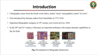
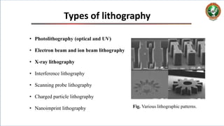
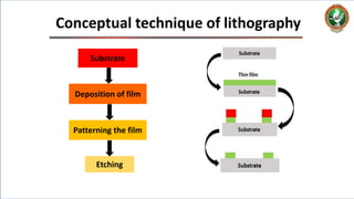
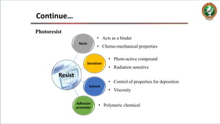
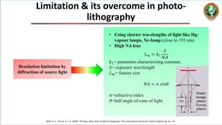
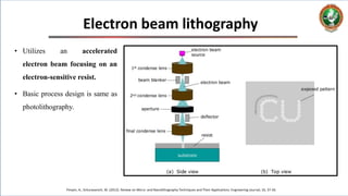
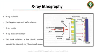
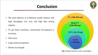
Visvesvaraya Technological University
Centre for Post-Graduate Studies
Muddenahalli, Bangalore- 562101
Design and Fabrication Techniques
Lithography Techniques
Presented by-
Kunal Roy
Department Nanoscience and Technology
M. Tech, 2nd Sem, USN: 1VW18INT02
Visvesvaraya Technological University
Centre for Post-Graduate Studies
Muddenahalli, Bangalore- 562101
Introduction
• Lithography comes from the Greek word, lithos, means "stone“ and graphein, means "to write”.
• First introduced by German author Alois Senefelder at 1771-1834.
• Important lithographic company of 19th century was Currier & Ives, 1852.
• In the 20th and 21st century, it becomes an important technique with unique dramatic capabilities in
the Art field.
Fig. Development in lithography dimensions.
Visvesvaraya Technological University
Centre for Post-Graduate Studies
Muddenahalli, Bangalore- 562101
Importance
• Low cost IC device manufacturing.
• Ultra-miniatured electronic device manufacturing.
• Widely used technique in microelectronic fabrication, particularly for
mass production of integrated circuits.
• Ability to register accurately over small area of a wafer.
M. Feldman, 2013, “Nanolithography, The Art of Fabricating Nanoelectronic and Nanophotonic Devices and Systems”,1st edition.
Fig. IC-devices as smaller
features.
Visvesvaraya Technological University
Centre for Post-Graduate Studies
Muddenahalli, Bangalore- 562101
Types of lithography
• Photolithography (optical and UV)
• Electron beam and ion beam lithography
• X-ray lithography
• Interference lithography
• Scanning probe lithography
• Charged particle lithography
• Nanoimprint lithography Fig. Various lithographic patterns.
Visvesvaraya Technological University
Centre for Post-Graduate Studies
Muddenahalli, Bangalore- 562101
Conceptual technique of lithography
Substrate
Deposition of film
Patterning the film
Etching
Visvesvaraya Technological University
Centre for Post-Graduate Studies
Muddenahalli, Bangalore- 562101
Photolithography
Cui, Z. (2007). Nanofabrication: Principles, Capabilities and Limits. Springer.
Hard bake
Final inspection
Basic steps
Visvesvaraya Technological University
Centre for Post-Graduate Studies
Muddenahalli, Bangalore- 562101
Cui, Z. (2007). Nanofabrication: Principles, Capabilities and Limits. Springer.
Mechanism
Continue…
Visvesvaraya Technological University
Centre for Post-Graduate Studies
Muddenahalli, Bangalore- 562101
Continue…
General
factors
Thickness of
resist
Mask
alignment
Wafer
surface
Resist
adhesion
Exposure
energy
Baking
temperature
Development
time
Types of
resist
Visvesvaraya Technological University
Centre for Post-Graduate Studies
Muddenahalli, Bangalore- 562101
Photoresist
Continue…
Resin
Sensitizer
Solvent
Adhesion
promoter
Resist
• Acts as a binder
• Chemo-mechanical properties
• Photo-active compound
• Radiation sensitive
• Control of properties for deposition
• Viscosity
• Polymeric chemical
Visvesvaraya Technological University
Centre for Post-Graduate Studies
Muddenahalli, Bangalore- 562101
Continue…
Cui, Z. (2007). Nanofabrication: Principles, Capabilities and Limits. Springer.
(A)
(B)
Types of resist
Visvesvaraya Technological University
Centre for Post-Graduate Studies
Muddenahalli, Bangalore- 562101
Limitation & its overcome in photo-
lithography
Mack, A. C., Tencor, K. L. A. (2004). The New, New Limits of Optical Lithography. The International Society for Optical Engineering. pp. 1-8.
Resolution limitation by
diffraction of source light
• Using shorter wavelengths of light like Hg-
vapour lamps, Xe-lamp (close to 193 nm)
• High NA lens
𝐿 𝑚 = 𝑘1
𝜆
𝑁𝐴
𝑘1= parameter characterizing constant,
𝜆= exposure wavelength
𝐿 𝑚= feature size
𝑁𝐴 = 𝑛 𝑠𝑖𝑛𝜃
𝑛=refractive index
𝜃=half angle of cone of light
Visvesvaraya Technological University
Centre for Post-Graduate Studies
Muddenahalli, Bangalore- 562101
Electron beam lithography
• Utilizes an accelerated
electron beam focusing on an
electron-sensitive resist.
• Basic process design is same as
photolithography.
Pimpin, A., Srituravanich, W. (2012). Review on Micro- and Nanolithography Techniques and Their Applications. Engineering Journal, 16, 37-56.
Visvesvaraya Technological University
Centre for Post-Graduate Studies
Muddenahalli, Bangalore- 562101
Continue…
Advantages
• High resolution up to 20 nm.
• Eliminates the diffraction problem.
• Print complex patterns directly on wafers.
Disadvantages
• Slower than optical lithography.
• Back scattering; secondary electrons
causes resolution problem.
Visvesvaraya Technological University
Centre for Post-Graduate Studies
Muddenahalli, Bangalore- 562101
X-ray lithography
• X-ray radiation.
• Gap between mask and wafer substrate.
• X-ray resists.
• X-ray masks are thinner.
• The mask substrate is low atomic number
material like diamond, beryllium or polyimide.
Y. Xia and G. M. Whitesides. (1998). Soft lithography. Annual Review of Materials Science, 28, 153-184.
Visvesvaraya Technological University
Centre for Post-Graduate Studies
Muddenahalli, Bangalore- 562101
Continue…
Advantages
• Shorter wavelength of 0.4 to 4 nm.
• No diffraction effect.
• Faster than EBL.
• Simple to use.
Disadvantages
• Very thin lens
• Distortion in absorber.
• Masks are expensive to produce.
• Vibration and time consuming.
Visvesvaraya Technological University
Centre for Post-Graduate Studies
Muddenahalli, Bangalore- 562101
Summary
Parameter Photolithography E-beam lithography X-ray lithography
Feature size 500 nm. 50 nm <10 nm
Resist Light sensitive Electron sensitive X-ray sensitive
Masks
Transparent fused silica with
chrome metal
Should not scatter electron.
Heavy metal absorber or thin
membrane used.
Throughput Very high Very low Very high
Diffraction Low resolution No No
Scattering No Yes No
Applications
Typical patterning in laboratory
level and production of various
MEMS devices
ICs production, patterning in R&D
including photonic crystals, channels for
nanofluidics
Manufacturing of multigate
devices such as FET, NEMS,
ICs and nanochips
Visvesvaraya Technological University
Centre for Post-Graduate Studies
Muddenahalli, Bangalore- 562101
Conclusion
• The main objective is to fabricate smaller features with
high throughput, low cost, and high data storing
capacity.
• To get better resolution, instrumental development is
necessary.
• Thin resist.
• Large numerical aperture.
• Shorter wavelength.
Deep UV
(150-250 nm)
UV (350-440 nm)
EUV (10-15 nm)
X-ray
(<10 nm)
Fig. Smaller Features with wavelengths.
Visvesvaraya Technological University
Centre for Post-Graduate Studies
Muddenahalli, Bangalore- 562101
Thank you

Lithography basics`

  • 1.
    Visvesvaraya Technological University Centrefor Post-Graduate Studies Muddenahalli, Bangalore- 562101 Design and Fabrication Techniques Lithography Techniques Presented by- Kunal Roy Department Nanoscience and Technology M. Tech, 2nd Sem, USN: 1VW18INT02
  • 2.
    Visvesvaraya Technological University Centrefor Post-Graduate Studies Muddenahalli, Bangalore- 562101 Introduction • Lithography comes from the Greek word, lithos, means "stone“ and graphein, means "to write”. • First introduced by German author Alois Senefelder at 1771-1834. • Important lithographic company of 19th century was Currier & Ives, 1852. • In the 20th and 21st century, it becomes an important technique with unique dramatic capabilities in the Art field. Fig. Development in lithography dimensions.
  • 3.
    Visvesvaraya Technological University Centrefor Post-Graduate Studies Muddenahalli, Bangalore- 562101 Importance • Low cost IC device manufacturing. • Ultra-miniatured electronic device manufacturing. • Widely used technique in microelectronic fabrication, particularly for mass production of integrated circuits. • Ability to register accurately over small area of a wafer. M. Feldman, 2013, “Nanolithography, The Art of Fabricating Nanoelectronic and Nanophotonic Devices and Systems”,1st edition. Fig. IC-devices as smaller features.
  • 4.
    Visvesvaraya Technological University Centrefor Post-Graduate Studies Muddenahalli, Bangalore- 562101 Types of lithography • Photolithography (optical and UV) • Electron beam and ion beam lithography • X-ray lithography • Interference lithography • Scanning probe lithography • Charged particle lithography • Nanoimprint lithography Fig. Various lithographic patterns.
  • 5.
    Visvesvaraya Technological University Centrefor Post-Graduate Studies Muddenahalli, Bangalore- 562101 Conceptual technique of lithography Substrate Deposition of film Patterning the film Etching
  • 6.
    Visvesvaraya Technological University Centrefor Post-Graduate Studies Muddenahalli, Bangalore- 562101 Photolithography Cui, Z. (2007). Nanofabrication: Principles, Capabilities and Limits. Springer. Hard bake Final inspection Basic steps
  • 7.
    Visvesvaraya Technological University Centrefor Post-Graduate Studies Muddenahalli, Bangalore- 562101 Cui, Z. (2007). Nanofabrication: Principles, Capabilities and Limits. Springer. Mechanism Continue…
  • 8.
    Visvesvaraya Technological University Centrefor Post-Graduate Studies Muddenahalli, Bangalore- 562101 Continue… General factors Thickness of resist Mask alignment Wafer surface Resist adhesion Exposure energy Baking temperature Development time Types of resist
  • 9.
    Visvesvaraya Technological University Centrefor Post-Graduate Studies Muddenahalli, Bangalore- 562101 Photoresist Continue… Resin Sensitizer Solvent Adhesion promoter Resist • Acts as a binder • Chemo-mechanical properties • Photo-active compound • Radiation sensitive • Control of properties for deposition • Viscosity • Polymeric chemical
  • 10.
    Visvesvaraya Technological University Centrefor Post-Graduate Studies Muddenahalli, Bangalore- 562101 Continue… Cui, Z. (2007). Nanofabrication: Principles, Capabilities and Limits. Springer. (A) (B) Types of resist
  • 11.
    Visvesvaraya Technological University Centrefor Post-Graduate Studies Muddenahalli, Bangalore- 562101 Limitation & its overcome in photo- lithography Mack, A. C., Tencor, K. L. A. (2004). The New, New Limits of Optical Lithography. The International Society for Optical Engineering. pp. 1-8. Resolution limitation by diffraction of source light • Using shorter wavelengths of light like Hg- vapour lamps, Xe-lamp (close to 193 nm) • High NA lens 𝐿 𝑚 = 𝑘1 𝜆 𝑁𝐴 𝑘1= parameter characterizing constant, 𝜆= exposure wavelength 𝐿 𝑚= feature size 𝑁𝐴 = 𝑛 𝑠𝑖𝑛𝜃 𝑛=refractive index 𝜃=half angle of cone of light
  • 12.
    Visvesvaraya Technological University Centrefor Post-Graduate Studies Muddenahalli, Bangalore- 562101 Electron beam lithography • Utilizes an accelerated electron beam focusing on an electron-sensitive resist. • Basic process design is same as photolithography. Pimpin, A., Srituravanich, W. (2012). Review on Micro- and Nanolithography Techniques and Their Applications. Engineering Journal, 16, 37-56.
  • 13.
    Visvesvaraya Technological University Centrefor Post-Graduate Studies Muddenahalli, Bangalore- 562101 Continue… Advantages • High resolution up to 20 nm. • Eliminates the diffraction problem. • Print complex patterns directly on wafers. Disadvantages • Slower than optical lithography. • Back scattering; secondary electrons causes resolution problem.
  • 14.
    Visvesvaraya Technological University Centrefor Post-Graduate Studies Muddenahalli, Bangalore- 562101 X-ray lithography • X-ray radiation. • Gap between mask and wafer substrate. • X-ray resists. • X-ray masks are thinner. • The mask substrate is low atomic number material like diamond, beryllium or polyimide. Y. Xia and G. M. Whitesides. (1998). Soft lithography. Annual Review of Materials Science, 28, 153-184.
  • 15.
    Visvesvaraya Technological University Centrefor Post-Graduate Studies Muddenahalli, Bangalore- 562101 Continue… Advantages • Shorter wavelength of 0.4 to 4 nm. • No diffraction effect. • Faster than EBL. • Simple to use. Disadvantages • Very thin lens • Distortion in absorber. • Masks are expensive to produce. • Vibration and time consuming.
  • 16.
    Visvesvaraya Technological University Centrefor Post-Graduate Studies Muddenahalli, Bangalore- 562101 Summary Parameter Photolithography E-beam lithography X-ray lithography Feature size 500 nm. 50 nm <10 nm Resist Light sensitive Electron sensitive X-ray sensitive Masks Transparent fused silica with chrome metal Should not scatter electron. Heavy metal absorber or thin membrane used. Throughput Very high Very low Very high Diffraction Low resolution No No Scattering No Yes No Applications Typical patterning in laboratory level and production of various MEMS devices ICs production, patterning in R&D including photonic crystals, channels for nanofluidics Manufacturing of multigate devices such as FET, NEMS, ICs and nanochips
  • 17.
    Visvesvaraya Technological University Centrefor Post-Graduate Studies Muddenahalli, Bangalore- 562101 Conclusion • The main objective is to fabricate smaller features with high throughput, low cost, and high data storing capacity. • To get better resolution, instrumental development is necessary. • Thin resist. • Large numerical aperture. • Shorter wavelength. Deep UV (150-250 nm) UV (350-440 nm) EUV (10-15 nm) X-ray (<10 nm) Fig. Smaller Features with wavelengths.
  • 18.
    Visvesvaraya Technological University Centrefor Post-Graduate Studies Muddenahalli, Bangalore- 562101 Thank you