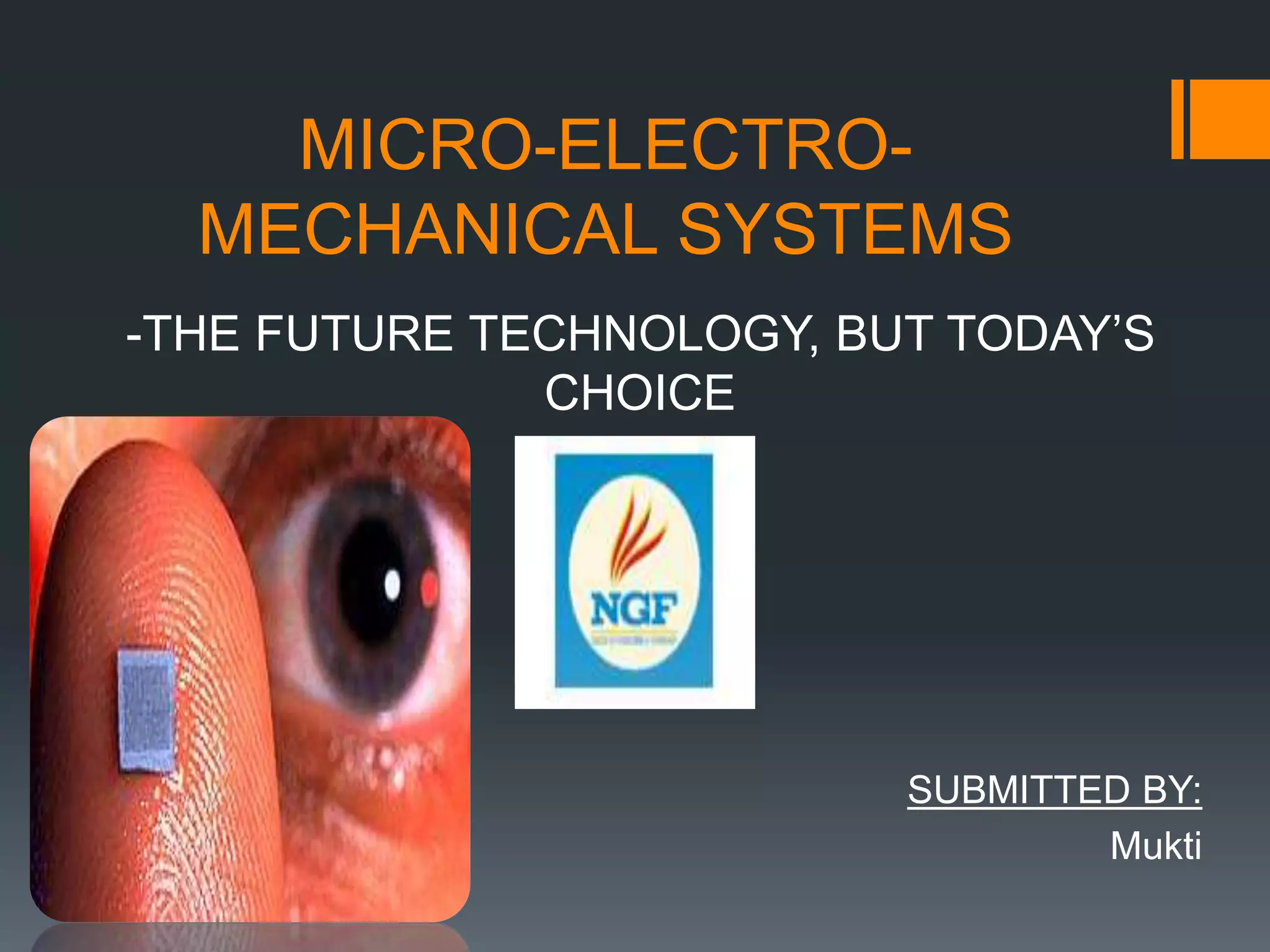
MICRO-ELECTRO-
MECHANICAL SYSTEMS
-THE FUTURE TECHNOLOGY, BUT TODAY’S
CHOICE
SUBMITTED BY:
Mukti
TABLE OF CONTENTS
1. INTRODUCTION
2. APPLICATIONS
3. ADVANTAGES AND DISADVANTAGES
4. CAD TOOLS USED FOR DESIGNING OF MEMS
5. FABRICATION PROCESS
6. MANUFACTURING PROCESS
7. CHALLENGES
8. CONCLUSION
9. REFERENCES
1.INTRODUCTION
MEMS or Micro-Electro Mechanical System is a technique of
combining Electrical and Mechanical components together on a
chip, to produce a system of miniature dimensions.
 Integration of a number of micro-components on a single chip
which allows the micro system to both sense and control the
environment.
 Made up of components between 1 to 100 micrometers in
size
 Devices generally range in size from 20 micrometers to a
millimeter.
MEMS
Micro
actuators
Micro
sensors
Micro
electronics
Micro
structures
COMPARISON: IC’S VS. MEMS
MEMS
 3D complex structures
 Doesn’t have any basic building
block
 May have moving parts
 May have interface with external
media
 Functions include
Biological,Chemical,Optical
 Packaging is very complex
IC
 2D structures
 Transistor is basic building block
 No moving parts
 Totally isolated with media
 Only Electrical
 Packaging Techniques are well
developed
WHAT IS A SENSOR?
 A device used to measure a physical
quantity(such as temperature) and
convert it into an electronic signal of
some kind(e.g. a voltage), without
modifying the environment.
What can be sensed?
Almost Everything!!!
Commonly sensed parameters are:
 Pressure
 Temperature
 Flow rate
 Radiation
 Chemicals
 Pathogens
N
S
EW
2 Axis
Magnetic
Sensor
2 Axis
Accelerometer
Light Intensity
Sensor
Humidity
Sensor
Pressure
Sensor
Temperature
Sensor
BUT WHY MEMS FOR SENSORS?
smaller in size
have lower power consumption
more sensitive to input variations
cheaper due to mass production
less invasive than larger devices
2. APPLICATIONS
• A MEMS is a device that can be
implanted in the human body.
• MEMS surgical tools provide the
flexibility and accuracy to perform
surgery.
• In medicine
• Biomems
Bio-mems are used to refer to the science
and technology of operating at the micro
scale for biological and biomedical
applications.
• In automotives :
• As gyroscope:
Heavy use of mems is found in air
bag systems, vehicle security
system, inertial brake lights,
rollover detection, automatic door
locks etc.
Inexpensive vibrating structure
gyroscopes manufactured with
mems technology have become
widely available. These are
packaged similarly to other integrated
circuits and may provide either analog
or digital outputs.
• In microphones:
Micro-electro mechanical system (MEMS)
technology help projectiles to reach their
targets accurately.
• In military :
The mems microphone also called
as microphone Chip is widely used
in the present day communication
world.
3. ADVANTAGES AND
DISADVANTAGES
 Minimize energy and
materials.
Improved
reproducibility.
 Improved accuracy
and reliability.
 Increased selectivity
and sensitivity.
 Farm establishment
requires huge
investments.
 Micro-components are
costly compared to
macro components.
 Design includes very
much complex
procedures
4 DESIGN TOOLS :CAD
In MEMS technology, CAD is defined as a
tightly organized set of cooperating computer
programs that enable the simulation of
manufacturing processes, device operation and
packaged Microsystems behavior in a
continuous sequence, by a Microsystems
engineer.
COMMERCIALLY AVAILABLE
SOFTWARE
Coventorware from Coventor
http://www.memcad.com
IntelliSuite from Intellisense Inc. (Corning)
http://www.intellisense.com
MEMS ProCAETool from Tanner Inc.
http://www.tanner.com
MEMScap from MEMScap Inc.
http://www.memscap.com
SOLIDIS from ISE Inc.
http://www.ise.com
EXAMPLE: INTELLISUITE
ADVANTAGES
• Design for manufacturability
– Fabrication database
– Thin-film materials engineering
– Virtual prototyping
• Ease of use
– Consistent user interface
– Communication with existing tools
• Accuracy
– MEMS-specific meshing and analysis engines
– In-house code development
– Validated by in-house MEMS designers
5. FABRICATION PROCESS
Deposition Patterning Etching
Physical Chemical Lithography Wet Dry
Photolithography
Electron beam lithography
Ion beam lithography
Ion track technology
X-ray lithography.
DEPOSITION
MEMS deposition technology can be classified in two
groups:
1. Depositions that happen because of a chemical reaction:
 Chemical Vapour Deposition (CVD)
 Electro deposition
 Epitaxy
 Thermal oxidation
2. Depositions that happen because of a physical reaction:
 Physical Vapour Deposition (PVD)
 Casting
PATTERNING
 Patterning of MEMS is the transfer of a pattern into a
material.
 Lithography is a widely used process
 Examples of lithography are– Photolithography, Electron
beam lithography, Ion beam lithography, Ion track
technology, X-ray lithography.
L
i
t
h
o
g
r
a
p
h
y
ETCHING
 Etching is the process of using strong acid to cut the
unprotected parts of a metal surface to create a design in.
 There are two classes of etching processes:
Wet Etching
Dry Etching.
6. MANUFACTURING
TECHNOLOGIES
Bulk Micromachining
Surface Micromachining
High Aspect Ratio (HAR) Silicon
Micromachining
BULK MICROMACHINING
This technique involves the
selective removal of the
substrate material in order to
realize miniaturized mechanical
components.
A widely used bulk
micromachining technique in
MEMS is chemical wet
etching, which involves the
immersion of a substrate into a
solution of reactive chemical
that will etch exposed regions
of the substrate at very high
rates.
Etched grooves using
(a) Anisotropic etchants,
(b) Isotropic etchants,
(c) Reactive Ion Etching
SURFACE MICROMACHINING
LIGA PROCESS
 LIGA is a German acronym standing for lithography,
galvanoformung (plating) and abformung (molding).
Polymethyl methacrylate (PMMA) is applied as photoresist to the
substrate by a glue-down process.
7. CHALLENGES
Design and
Packaging
Testing
Sensing Latching
Controllability Reliability
8. CONCLUSION
MEMS promises to be an effective technique of producing
sensors of high quality, at lower costs.
Thus we can conclude that the MEMS can create a proactive
computing world, connected computing nodes automatically,
acquire and act on real-time data about a physical environment,
helping to improve lives, promoting a better understanding of
the world and enabling people to become more productive.
9. REFERENCES
Christian A. Zorman, Mehran Mehregany, MEMS Design and
Fabrication, 2nd Ed. 2,16.
Ms. Santoshi Gupta, MEMS and Nanotechnology IJSER, Vol 3,
Issue 5,2012
R. Ghodssi, P. Lin (2011). MEMS Materials and Processes
Handbook. Berlin: Springer.
Chang, Floy I. (1995).Gas-phase silicon micromachining with
xenon difluoride. 2641. pp. 117.
. Micromechanics and MEMS: Classic and Seminal Paper to
1990, Trimmer, W.S., IEEE Press, New York, NY, 1997.
Journal of Microelectromechanical Systems
(http://www.ieee.org/pub_preview/mems_toc.html)
University of Stanford,
http://www.stanford.edu/group/SML/ee321/ho/MEMS-01-
intro.pdf
Trimmer, W.S., Micromechanics and MEMS: Classic and
Seminal Papers to 1990, IEEE Press, New York, NY, 1997.
Tjerkstra, R. W., de Boer, M., Berenschot, E., Gardeniers,
J.G.E., van der Berg, A., and Elwenspoek, M., Etching
Technology for Microchannels, Proceedings of the 10th Annual
Workshop of Micro Electro Mechanical Systems (MEMS ’97),
Nagoya, Japan, Jan. 26-30, 1997, pp. 396-398.
THANK YOU

Mems ppt

  • 1.
    MICRO-ELECTRO- MECHANICAL SYSTEMS -THE FUTURETECHNOLOGY, BUT TODAY’S CHOICE SUBMITTED BY: Mukti
  • 2.
    TABLE OF CONTENTS 1.INTRODUCTION 2. APPLICATIONS 3. ADVANTAGES AND DISADVANTAGES 4. CAD TOOLS USED FOR DESIGNING OF MEMS 5. FABRICATION PROCESS 6. MANUFACTURING PROCESS 7. CHALLENGES 8. CONCLUSION 9. REFERENCES
  • 3.
    1.INTRODUCTION MEMS or Micro-ElectroMechanical System is a technique of combining Electrical and Mechanical components together on a chip, to produce a system of miniature dimensions.  Integration of a number of micro-components on a single chip which allows the micro system to both sense and control the environment.
  • 4.
     Made upof components between 1 to 100 micrometers in size  Devices generally range in size from 20 micrometers to a millimeter.
  • 5.
  • 6.
    COMPARISON: IC’S VS.MEMS MEMS  3D complex structures  Doesn’t have any basic building block  May have moving parts  May have interface with external media  Functions include Biological,Chemical,Optical  Packaging is very complex IC  2D structures  Transistor is basic building block  No moving parts  Totally isolated with media  Only Electrical  Packaging Techniques are well developed
  • 7.
    WHAT IS ASENSOR?  A device used to measure a physical quantity(such as temperature) and convert it into an electronic signal of some kind(e.g. a voltage), without modifying the environment. What can be sensed? Almost Everything!!! Commonly sensed parameters are:  Pressure  Temperature  Flow rate  Radiation  Chemicals  Pathogens N S EW 2 Axis Magnetic Sensor 2 Axis Accelerometer Light Intensity Sensor Humidity Sensor Pressure Sensor Temperature Sensor
  • 8.
    BUT WHY MEMSFOR SENSORS? smaller in size have lower power consumption more sensitive to input variations cheaper due to mass production less invasive than larger devices
  • 9.
    2. APPLICATIONS • AMEMS is a device that can be implanted in the human body. • MEMS surgical tools provide the flexibility and accuracy to perform surgery. • In medicine • Biomems Bio-mems are used to refer to the science and technology of operating at the micro scale for biological and biomedical applications.
  • 10.
    • In automotives: • As gyroscope: Heavy use of mems is found in air bag systems, vehicle security system, inertial brake lights, rollover detection, automatic door locks etc. Inexpensive vibrating structure gyroscopes manufactured with mems technology have become widely available. These are packaged similarly to other integrated circuits and may provide either analog or digital outputs.
  • 11.
    • In microphones: Micro-electromechanical system (MEMS) technology help projectiles to reach their targets accurately. • In military : The mems microphone also called as microphone Chip is widely used in the present day communication world.
  • 12.
    3. ADVANTAGES AND DISADVANTAGES Minimize energy and materials. Improved reproducibility.  Improved accuracy and reliability.  Increased selectivity and sensitivity.  Farm establishment requires huge investments.  Micro-components are costly compared to macro components.  Design includes very much complex procedures
  • 13.
    4 DESIGN TOOLS:CAD In MEMS technology, CAD is defined as a tightly organized set of cooperating computer programs that enable the simulation of manufacturing processes, device operation and packaged Microsystems behavior in a continuous sequence, by a Microsystems engineer.
  • 14.
    COMMERCIALLY AVAILABLE SOFTWARE Coventorware fromCoventor http://www.memcad.com IntelliSuite from Intellisense Inc. (Corning) http://www.intellisense.com MEMS ProCAETool from Tanner Inc. http://www.tanner.com MEMScap from MEMScap Inc. http://www.memscap.com SOLIDIS from ISE Inc. http://www.ise.com
  • 15.
    EXAMPLE: INTELLISUITE ADVANTAGES • Designfor manufacturability – Fabrication database – Thin-film materials engineering – Virtual prototyping • Ease of use – Consistent user interface – Communication with existing tools • Accuracy – MEMS-specific meshing and analysis engines – In-house code development – Validated by in-house MEMS designers
  • 16.
    5. FABRICATION PROCESS DepositionPatterning Etching Physical Chemical Lithography Wet Dry Photolithography Electron beam lithography Ion beam lithography Ion track technology X-ray lithography.
  • 18.
    DEPOSITION MEMS deposition technologycan be classified in two groups: 1. Depositions that happen because of a chemical reaction:  Chemical Vapour Deposition (CVD)  Electro deposition  Epitaxy  Thermal oxidation 2. Depositions that happen because of a physical reaction:  Physical Vapour Deposition (PVD)  Casting
  • 19.
    PATTERNING  Patterning ofMEMS is the transfer of a pattern into a material.  Lithography is a widely used process  Examples of lithography are– Photolithography, Electron beam lithography, Ion beam lithography, Ion track technology, X-ray lithography.
  • 20.
  • 21.
    ETCHING  Etching isthe process of using strong acid to cut the unprotected parts of a metal surface to create a design in.  There are two classes of etching processes: Wet Etching Dry Etching.
  • 22.
    6. MANUFACTURING TECHNOLOGIES Bulk Micromachining SurfaceMicromachining High Aspect Ratio (HAR) Silicon Micromachining
  • 23.
    BULK MICROMACHINING This techniqueinvolves the selective removal of the substrate material in order to realize miniaturized mechanical components. A widely used bulk micromachining technique in MEMS is chemical wet etching, which involves the immersion of a substrate into a solution of reactive chemical that will etch exposed regions of the substrate at very high rates. Etched grooves using (a) Anisotropic etchants, (b) Isotropic etchants, (c) Reactive Ion Etching
  • 25.
  • 26.
    LIGA PROCESS  LIGAis a German acronym standing for lithography, galvanoformung (plating) and abformung (molding). Polymethyl methacrylate (PMMA) is applied as photoresist to the substrate by a glue-down process.
  • 27.
    7. CHALLENGES Design and Packaging Testing SensingLatching Controllability Reliability
  • 28.
    8. CONCLUSION MEMS promisesto be an effective technique of producing sensors of high quality, at lower costs. Thus we can conclude that the MEMS can create a proactive computing world, connected computing nodes automatically, acquire and act on real-time data about a physical environment, helping to improve lives, promoting a better understanding of the world and enabling people to become more productive.
  • 29.
    9. REFERENCES Christian A.Zorman, Mehran Mehregany, MEMS Design and Fabrication, 2nd Ed. 2,16. Ms. Santoshi Gupta, MEMS and Nanotechnology IJSER, Vol 3, Issue 5,2012 R. Ghodssi, P. Lin (2011). MEMS Materials and Processes Handbook. Berlin: Springer. Chang, Floy I. (1995).Gas-phase silicon micromachining with xenon difluoride. 2641. pp. 117. . Micromechanics and MEMS: Classic and Seminal Paper to 1990, Trimmer, W.S., IEEE Press, New York, NY, 1997. Journal of Microelectromechanical Systems (http://www.ieee.org/pub_preview/mems_toc.html)
  • 30.
    University of Stanford, http://www.stanford.edu/group/SML/ee321/ho/MEMS-01- intro.pdf Trimmer,W.S., Micromechanics and MEMS: Classic and Seminal Papers to 1990, IEEE Press, New York, NY, 1997. Tjerkstra, R. W., de Boer, M., Berenschot, E., Gardeniers, J.G.E., van der Berg, A., and Elwenspoek, M., Etching Technology for Microchannels, Proceedings of the 10th Annual Workshop of Micro Electro Mechanical Systems (MEMS ’97), Nagoya, Japan, Jan. 26-30, 1997, pp. 396-398.
  • 31.