Downloaded 237 times


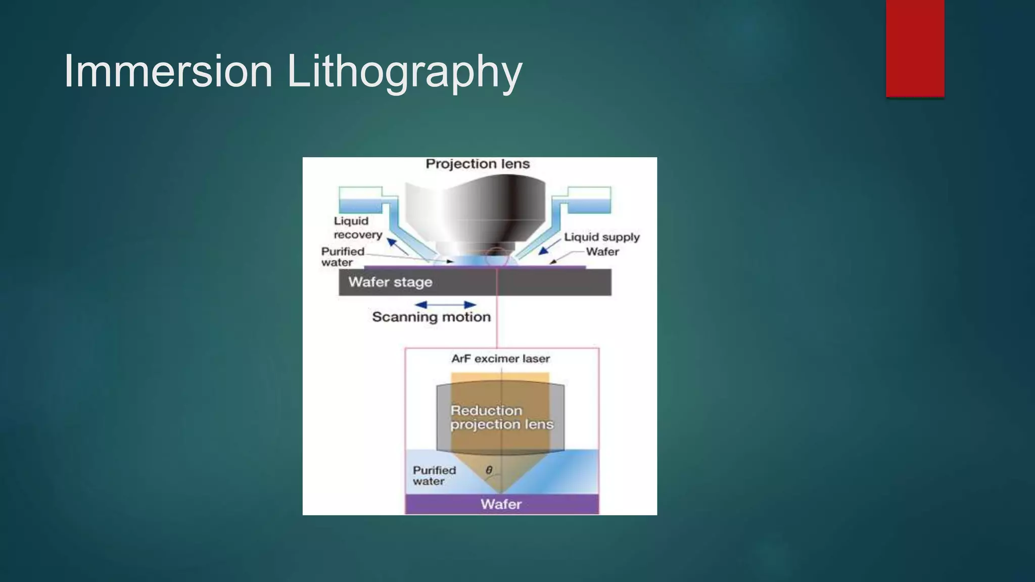


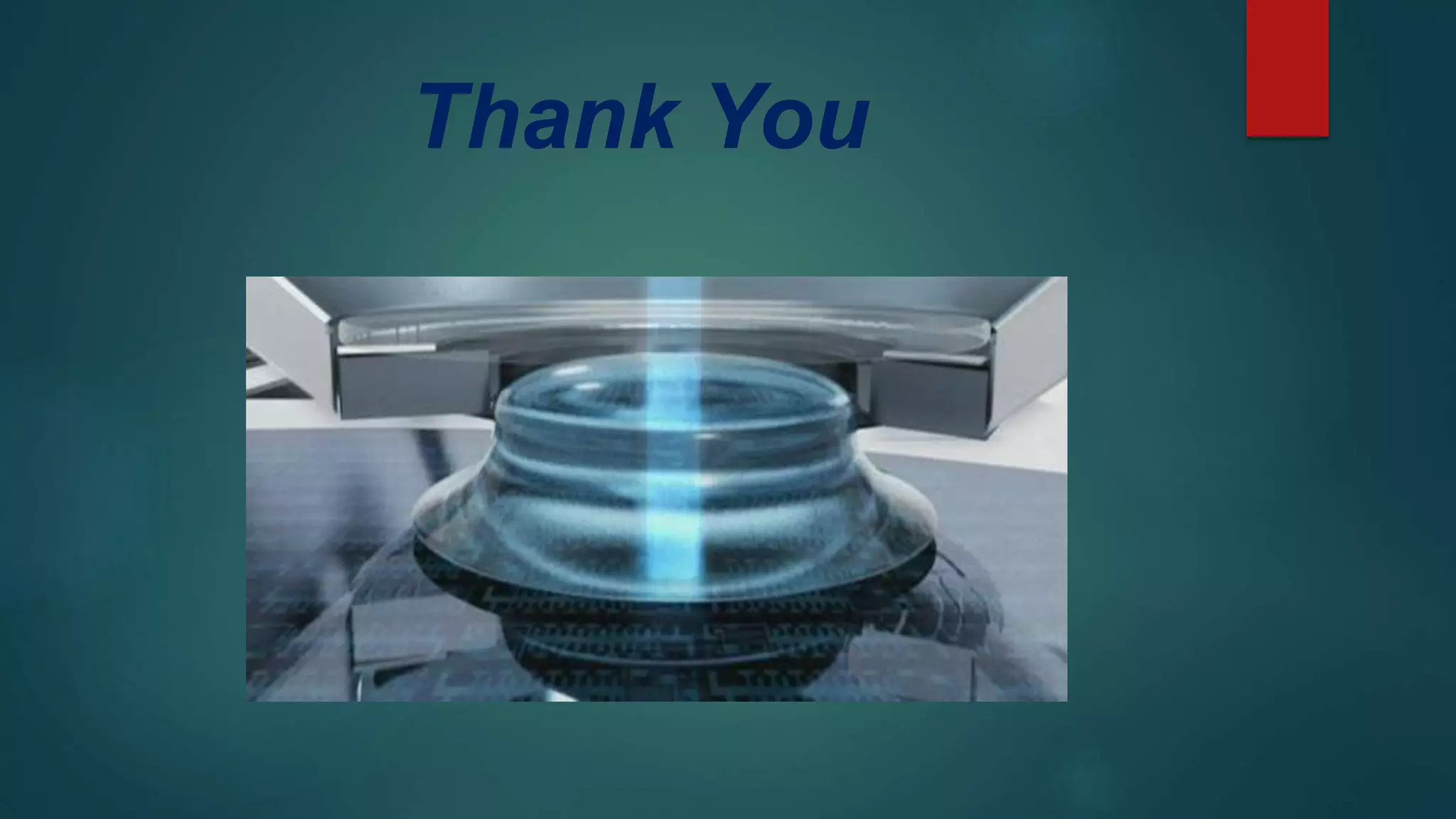

Immersion lithography is a technique used in photolithography to enhance resolution. It works by placing a liquid such as water between the final optical element of the lithography system and the wafer. This allows higher numerical apertures compared to conventional "dry" lithography in air. The higher numerical aperture enables printing of smaller features. While it provides advantages, immersion lithography also presents challenges such as bubbles in the immersion liquid and interactions between the liquid and photoresist. It is widely adopted by semiconductor manufacturers for sub-45nm node fabrication.


