Downloaded 1,431 times
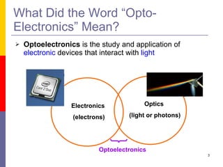
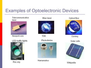
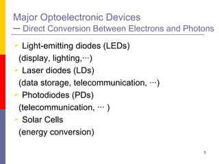

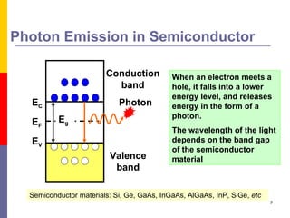
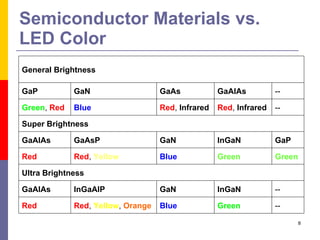
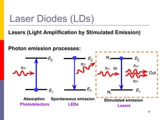
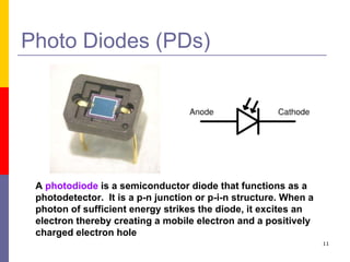
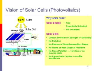
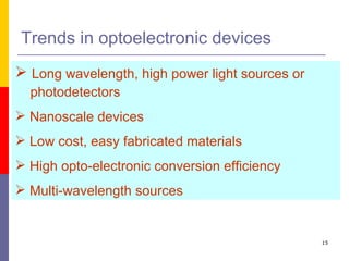
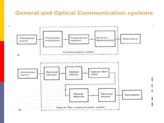

This document discusses optoelectronic devices and provides examples. It introduces optoelectronics as the study of electronic devices that interact with light. Major optoelectronic devices directly convert between electrons and photons, including light-emitting diodes (LEDs), laser diodes, and photodiodes. LEDs emit light when electrically biased and the color depends on the semiconductor material. Laser diodes use stimulated emission to produce coherent light. Photodiodes are photodetectors that generate a current when struck by photons. The document also discusses solar cells and trends in optoelectronic devices.


