Downloaded 145 times

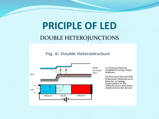
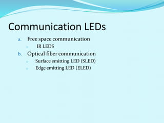
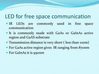
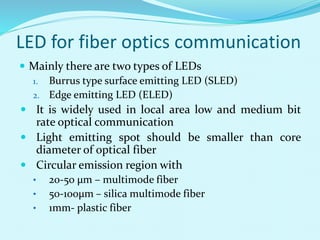

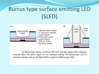
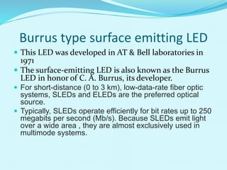
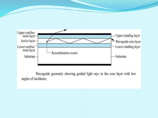
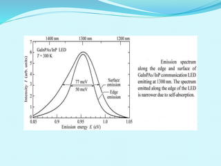
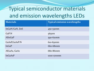
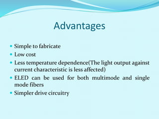

This document discusses double heterojunction LEDs and their use in optical fiber communication. It explains that a double heterojunction structure sandwiches a small bandgap semiconductor between two large bandgap semiconductors. This reduces light losses by emitting photons from the small bandgap region. Surface emitting LEDs and edge emitting LEDs are described as the main types used for fiber optic communication over short distances and low data rates. Common semiconductor materials and their emission wavelengths are also listed.


