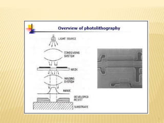
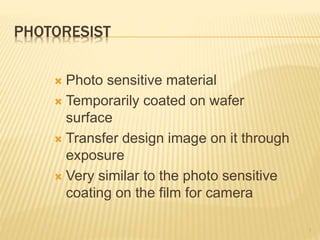
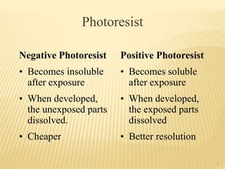
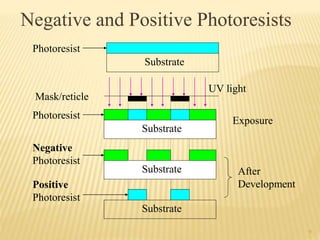
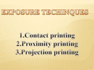
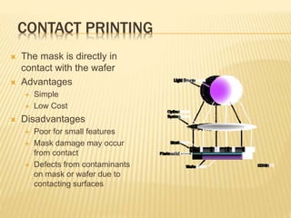
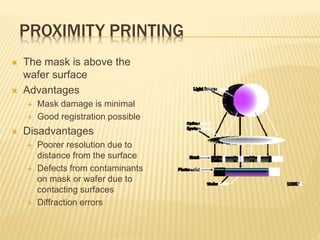
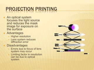
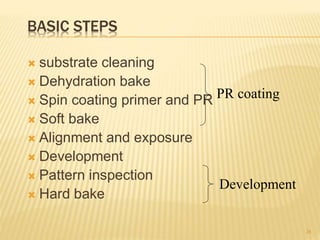
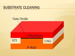
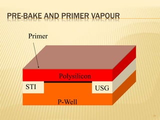
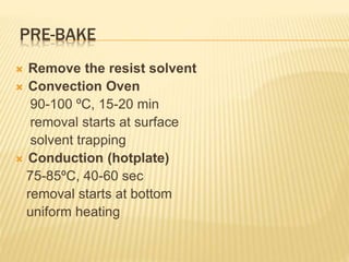
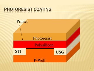
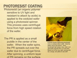
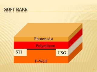
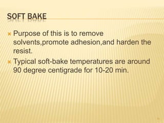
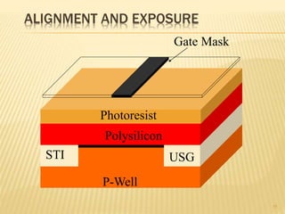
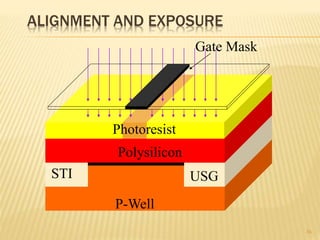
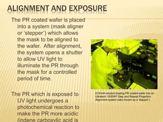
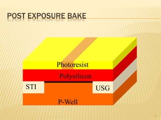
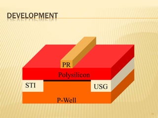
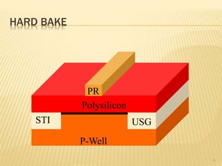
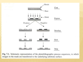
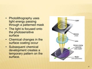
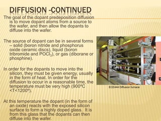
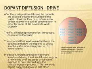
The document describes the process of photolithography used in integrated circuit manufacturing. Photolithography involves coating a wafer with photoresist, exposing it to UV light through a mask to transfer the mask pattern, and developing the photoresist to remove the exposed or unexposed areas. Key steps include cleaning the wafer, applying and soft baking the photoresist, aligning and exposing the wafer through the mask, developing the pattern, and etching or implanting areas not protected by the photoresist. Photolithography is critical for patterning layers in chip fabrication and determining the minimum feature size.