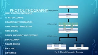
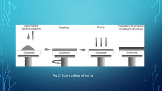
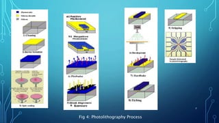
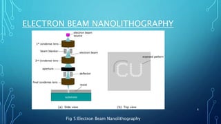
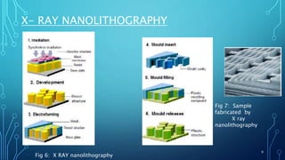
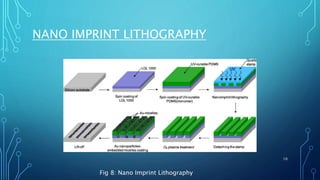
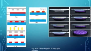
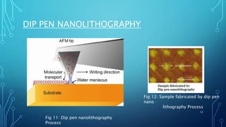
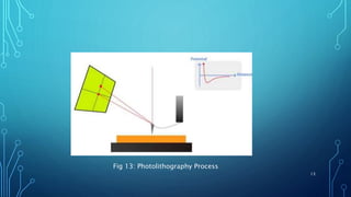
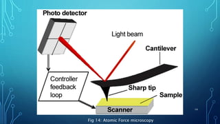
NANOLITHOGRAPHY
TECHNIQUES
FOR NANO SCALE
FABRICATION
DONE BY:
GIRISH RAGHUNATHAN
1RV18MMD07 1
OUTLINE
• Introduction
• Photolithography
• Electron Beam Lithography
• X Ray Lithography
• Nano imprint Lithography
• Dip pen lithography
2
INTRODUCTION
• Nanolithography is the branch of nanotechnology concerned
with the study and application of fabricating nanometer-scale
structures.
• Nanos –dwarf
• Lithos- stone
• Graphein- to write
• Roughly nanolithography translates into ‘tiny writing on stone’
3
PHOTOLITHOGRAPHY
4
STEPS IN PHOTOLITHOGRAPHY :
1) WATER CLEANING
2) BARRIER LAYER FORMATION
3) PHOTORESIST APPLICATION
4) PRE BAKING
5) MASK ALIGNMENT AND EXPOSURE
6) DEVELOPMENT
7) HARD BAKING
8) ETCHING
9) STRIPPING Fig 1: Photolithography Process
5
Fig 2: Spin coating of resist
6
Fig 3: Photolithography Process
7
Fig 4: Photolithography Process
ELECTRON BEAM NANOLITHOGRAPHY
8
Fig 5:Electron Beam Nanolithography
X- RAY NANOLITHOGRAPHY
9
Fig 6: X RAY nanolithography
Fig 7: Sample
fabricated by
X ray
nanolithography
NANO IMPRINT LITHOGRAPHY
10
Fig 8: Nano Imprint Lithography
11
Fig 9,10: Nano imprint lithography
DIP PEN NANOLITHOGRAPHY
12
Fig 11: Dip pen nanolithography
Process
Fig 12: Sample fabricated by dip pen
nano
lithography Process
13
Fig 13: Photolithography Process
14
Fig 14: Atomic Force microscopy
REFERENCES
• M. Feldman, 2013, “Nanolithography, The Art of Fabricating
Nanoelectronic and Nanophotonic Devices and Systems”,1st
edition.
• Dhara Parikh, Barry Craver, Hatem N. Nounu, Fu-On Fong, and
John C. Wolfe, "Nanoscale Pattern Definition on Nonplanar
Surfaces Using Ion Beam Proximity Lithography and Conformal
Plasma-Deposited Resist", Journal of Microelectromechanical
Systems, VOL. 17, NO. 3, JUNE 2008
15
16

Nano lithography techniques